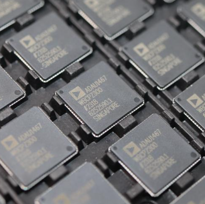
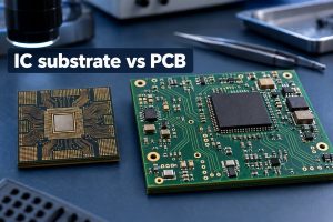
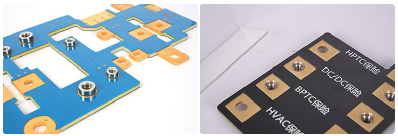
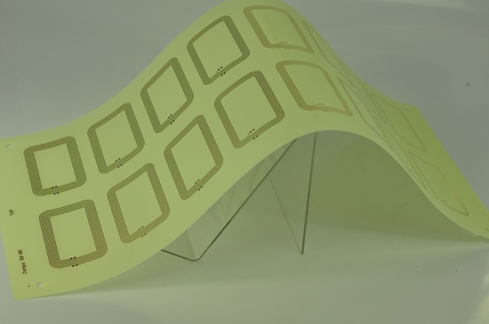
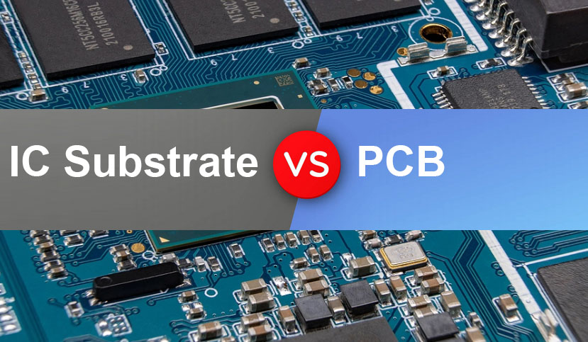
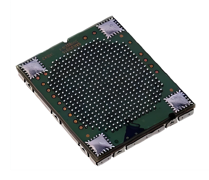
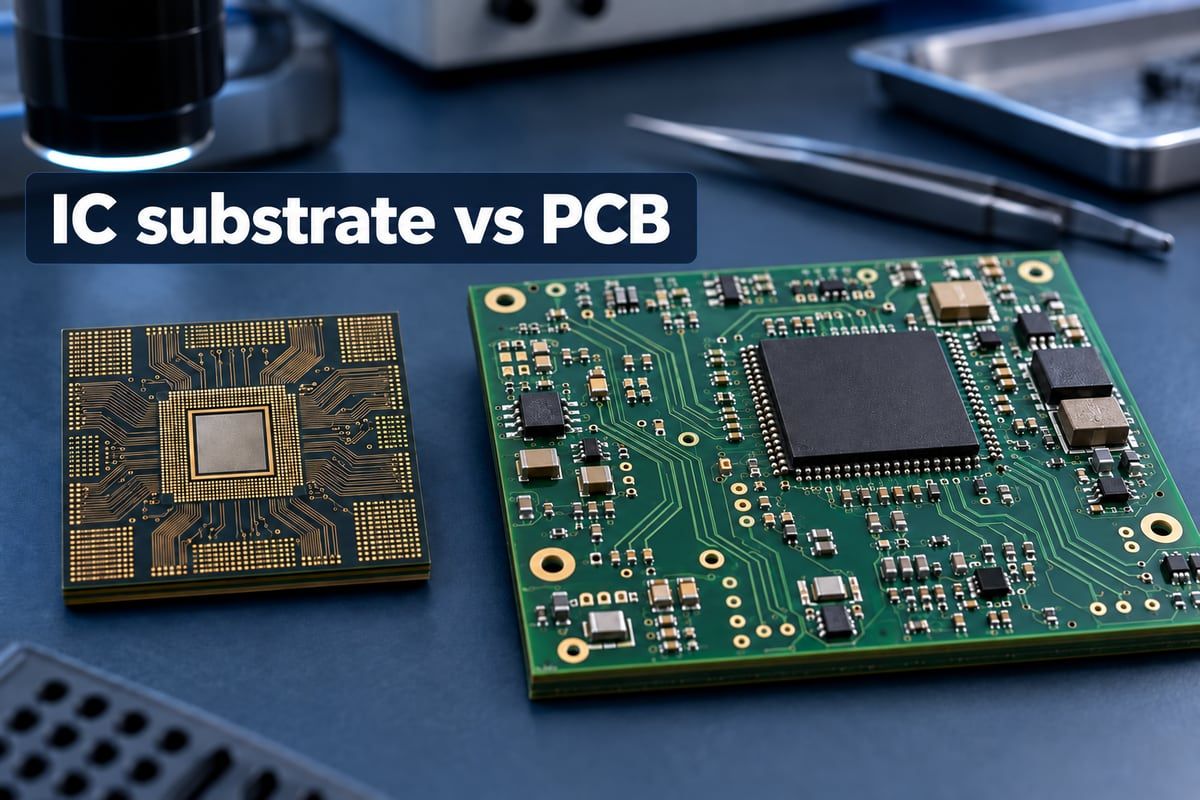
In an IC substrate vs PCB comparison, the two may look similar because both contain patterned copper conductors, insulating materials, vias, and multiple layers. However, they perform different jobs at different levels of an electronic system. An IC substrate connects a semiconductor die to the next level of packaging or to a PCB, while the PCB connects the packaged IC to memory, power devices, connectors, sensors, and other components.
Understanding this distinction helps engineers and sourcing teams avoid treating an IC substrate as simply a smaller PCB. The differences affect materials, conductor geometry, via technology, registration, inspection, manufacturing yield, and supplier selection.
EBest Circuit supports customers with IC substrate and PCB manufacturability review, material and stackup coordination, precision fabrication, inspection, and production planning. If you are comparing the two technologies for an upcoming project, send your drawings, stackup, critical dimensions, and volume requirements to sales@bestpcbs.com for an initial manufacturing review.
What Is an IC Substrate?
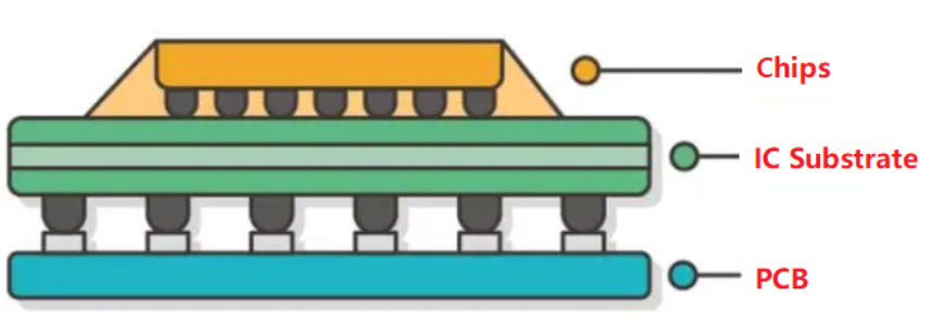
An IC substrate is the interconnection platform that supports a semiconductor die and connects its dense array of terminals to larger, more widely spaced connections. It is commonly located inside an IC package, between the die and the main PCB.
The substrate performs several jobs at once:
- It mechanically supports the semiconductor die.
- It redistributes very fine die-level connections to a larger connection pattern.
- It carries power and electrical signals between the die and the PCB.
- It provides controlled electrical paths for high-speed or high-frequency signals.
- It contributes to heat transfer and package reliability.
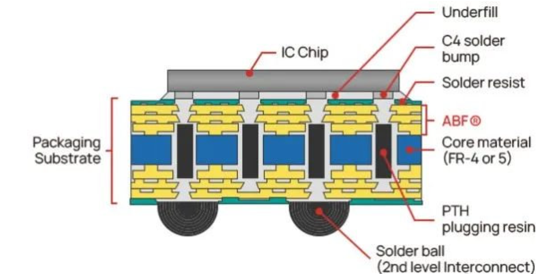
Depending on the package, the die may connect to the substrate through wire bonding or flip-chip interconnection. The substrate may then connect to the system PCB through a ball grid array or another package interface.
IC substrates can be made with organic build-up materials, BT resin systems, ceramics, or other specialized material systems. The appropriate construction depends on the package architecture, interconnection density, electrical requirements, thermal behavior, and reliability target.
An IC substrate is therefore not the chip itself and is not the main system board. It is the high-density bridge that allows a small semiconductor die to communicate with the larger electronic assembly.
Where Do IC Substrates and PCBs Fit in an Electronic System?
The easiest way to understand the distinction is to follow the electrical path from the chip to the finished product:
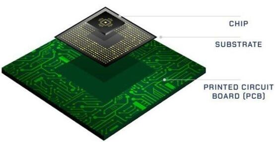
Semiconductor die → IC substrate → packaged IC → PCB → complete electronic system
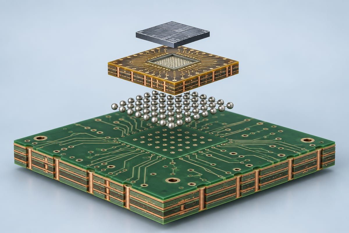
The IC substrate works at the package level. It handles the transition from extremely small die connections to package-level terminals. The PCB works at the board and system level. It routes signals and power among the packaged IC and the rest of the electronic components.
The IC substrate focuses on one semiconductor package. Its design is closely tied to the die, package format, bump or bond-pad arrangement, and package reliability requirements.
The PCB supports the wider circuit. It connects processors, memory, power-management devices, connectors, passive components, sensors, and other packages required by the product.
This means the two technologies are usually complementary rather than competing choices. A processor may require an IC substrate inside its package and a multilayer PCB beneath that package. Removing either interconnection level would require a different package and system architecture—not a simple material substitution.
For customers, the practical implication is that the substrate and PCB cannot be specified independently when signal integrity, power delivery, thermomechanical behavior, or escape routing is critical. Their interface must be considered early enough to avoid incompatible pad geometries, stackups, assembly profiles, or reliability assumptions.
IC Substrate vs PCB: Key Differences at a Glance
The most important difference is scale. An IC substrate manages dense package-level interconnections close to the semiconductor die; a PCB manages board-level connections across the product.
| Comparison | IC substrate | PCB |
|---|---|---|
| Primary role | Connects and supports a semiconductor die | Connects packaged components in a circuit |
| System position | Inside or directly beneath the IC package | Main board or functional circuit board |
| Interconnection density | Very high | Varies from conventional to advanced HDI |
| Typical conductor geometry | Finer lines, spaces, pads, and vias | Generally larger, depending on PCB technology |
| Material focus | Package-level electrical, thermal, and dimensional demands | Board-level electrical, mechanical, and assembly demands |
| Manufacturing control | Very tight registration and defect control | Broad range from standard PCB to advanced HDI control |
| Design dependency | Closely tied to die and package architecture | Closely tied to system circuit and component placement |
These are general distinctions, not universal dimensional limits. Advanced HDI and substrate-like PCBs can use features much smaller than conventional PCBs, while different IC substrate technologies have different capabilities. The actual manufacturing boundary must be established from the proposed stackup and feature sizes.
How Do IC Substrate and PCB Structures Differ?
Both products can use multilayer constructions, but their structures are optimized for different interconnection levels.
An organic IC substrate often uses a core with fine-feature build-up layers on one or both sides. Microvias connect the build-up layers, while the routing redistributes die-side connections toward the package interface. Some advanced constructions may be coreless or use other specialized architectures.
A PCB may use plated through holes, buried vias, blind vias, stacked or staggered microvias, and sequential lamination. Its construction is selected around component escape routing, controlled impedance, power distribution, mechanical thickness, assembly, and product-level reliability.
The structural difference customers should notice is the transition in connection scale. The die-facing side of an IC substrate must accommodate a much denser terminal pattern than a typical component-facing PCB layer. That density drives finer conductors, smaller vias, tighter alignment, and more demanding inspection.
It is also important not to confuse an IC substrate with a substrate-like PCB. Substrate-like PCB technology narrows the gap between advanced HDI PCBs and package substrates by using finer board-level features. However, its role, production flow, and qualification requirements still depend on the specific product architecture. The terms should not be treated as interchangeable without reviewing the actual construction.
Before requesting a quotation, customers should identify which interface each drawing represents: die side, package side, component side, or system-board side. That one clarification prevents many incorrect capability comparisons.
What Materials Are Used in IC Substrates and PCBs?
Material selection follows the function of each product.
Organic IC substrates commonly use BT resin or ABF-based build-up materials, along with copper conductors and application-specific core materials. Ceramic substrates may use alumina, aluminum nitride, or other ceramic systems when thermal, dimensional, environmental, or electrical requirements justify them.
PCBs commonly use FR-4-class laminates, but that description covers a wide range of resin systems and glass constructions. High-speed, high-frequency, high-temperature, metal-core, flexible, and rigid-flex PCBs use different material families according to their operating requirements.
For an IC substrate, material decisions are closely tied to the package. Important factors can include dimensional stability, coefficient of thermal expansion, dielectric behavior, moisture response, warpage, copper adhesion, and compatibility with the selected package process.
For a PCB, material decisions are tied to the assembled product. The designer may prioritize controlled impedance, signal loss, thermal performance, voltage isolation, mechanical strength, soldering temperature, operating environment, and cost.
Customers should avoid selecting materials from a generic name alone. A commercially familiar resin family does not guarantee that every supplier, thickness, copper configuration, or build-up process will produce equivalent results. The fabricator needs the electrical targets, mechanical constraints, thermal conditions, reliability expectations, and approved-material requirements before confirming a practical construction.
Why Does an IC Substrate Require Greater Manufacturing Precision?
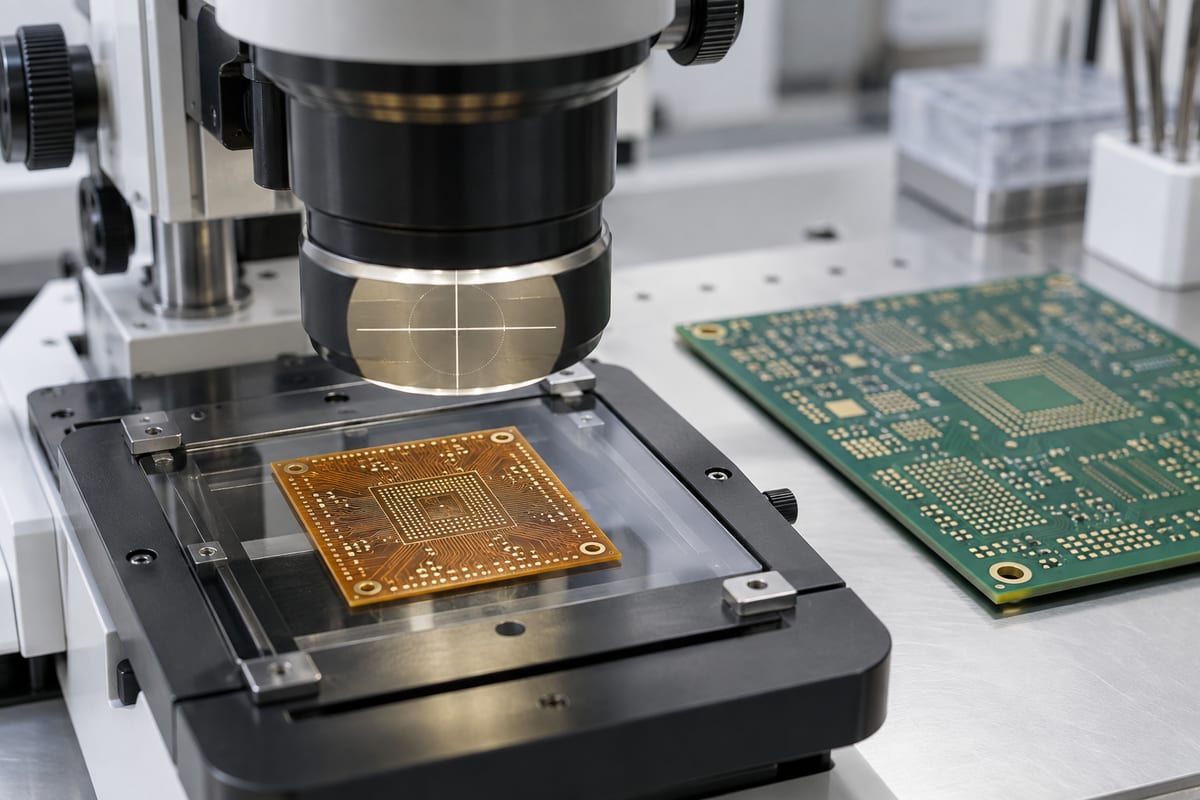
An IC substrate has to redistribute a large number of connections within a very small area. As die I/O density increases, the available routing space becomes more limited and small manufacturing variations consume a larger part of the tolerance budget.
Greater precision is normally required in several areas:
- Fine lines and spaces: Dense routing demands narrower conductors and smaller separations.
- Small microvias: Compact interconnections require carefully controlled via formation, metallization, and capture-pad alignment.
- Layer registration: Small pads and conductors leave less room for layer-to-layer misalignment.
- Dielectric thickness: Variations can affect impedance, via geometry, and overall package thickness.
- Surface quality: Fine-pitch connections require suitable flatness, cleanliness, and finish control.
- Warpage: Excessive deformation can interfere with die attachment, package assembly, or board-level soldering.
- Defect detection: Small opens, shorts, voids, residues, and registration errors may require higher-resolution inspection.
These controls affect both feasibility and yield. A design may look complete in CAD but still be unsuitable for stable production if its minimum features sit too close to the supplier’s process limits across a large area or high layer count.
The customer benefit of an early manufacturability review is therefore not merely getting the design “approved.” It is identifying where tolerances, via structures, pad sizes, material behavior, or inspection limits could create yield and reliability risk before those risks become embedded in tooling and production.
How Does IC Substrate Manufacturing Differ from PCB Manufacturing?
Both manufacturing flows build patterned conductors and interlayer connections, but the equipment, process windows, materials, and control levels can differ substantially.
Conventional PCB production may include laminate preparation, imaging, etching, drilling, plating, lamination, solder-mask application, surface finishing, electrical testing, and final inspection. Advanced HDI PCB production adds sequential build-up cycles, laser-drilled microvias, via filling, tighter registration, and finer imaging.
IC substrate manufacturing generally pushes these controls further toward package-level feature density. Depending on the construction, production may involve repeated build-up formation, fine-feature patterning, microvia creation, copper deposition and plating, precision lamination, surface treatment, and high-resolution inspection.
The main manufacturing differences affect the customer’s project in four ways:
- Design rules: Minimum conductors, spaces, via sizes, annular structures, and registration allowances must match the specific process.
- Yield sensitivity: A small feature repeated thousands of times can become a meaningful yield driver.
- Tooling and inspection: Finer features may require different imaging, drilling, metrology, and defect-detection capability.
- Qualification and lead time: Material approval, process validation, samples, and reliability testing may require more planning than a standard PCB order.
Customers should compare suppliers using the proposed construction—not a general statement that a factory can manufacture “fine-pitch boards.” Useful evidence includes capability matched to the required stackup, demonstrated control of the critical feature, appropriate inspection methods, and a realistic prototype-to-volume plan.
Can a PCB Replace an IC Substrate?
In most conventional package architectures, no. A standard PCB is not a direct replacement for the IC substrate because it is designed for a different interconnection level.
The substrate must accept the die-side connection pattern, redistribute those connections, satisfy package-level mechanical and electrical requirements, and provide a suitable interface to the PCB. A conventional PCB normally does not provide the necessary combination of feature density, package geometry, material behavior, and assembly compatibility.
Advanced HDI or substrate-like PCB technologies can reduce the dimensional gap in certain applications. That does not automatically make them interchangeable with a package substrate. The decision depends on:
- Die or package interconnection method
- Required line, space, pad, and microvia geometry
- Layer count and routing density
- Electrical and power-delivery targets
- Package thickness and warpage limits
- Thermal and coefficient-of-expansion behavior
- Assembly and reliability requirements
- Qualified manufacturing process
The better question is not, “Can we use a cheaper PCB instead?” It is, “Which interconnection architecture satisfies the package, board, assembly, and reliability requirements with a manufacturable process?” Answering that question requires collaboration among the package designer, PCB designer, assembly provider, and fabricator.
How Do IC Substrates and PCBs Work Together?
The IC substrate and PCB form consecutive parts of the same electrical and mechanical path.
Signals and power travel from the semiconductor die through the substrate routing, across the package-to-board interface, and into the PCB. From there, the PCB distributes them to power circuits, memory, connectors, sensors, and other devices.
Because the two products meet at the package interface, several decisions must align:
- Pad and ball geometry: The PCB land pattern must match the packaged device.
- Escape routing: The PCB must route away from the package without violating impedance, spacing, or layer-transition requirements.
- Power delivery: Package and board power structures must work together to control voltage drop, noise, and current density.
- Signal integrity: The complete channel includes structures in both the substrate and PCB.
- Thermal behavior: Heat spreading, copper distribution, vias, heatsinks, and airflow belong to one thermal system.
- Warpage and assembly: Substrate, package, PCB, and solder-joint behavior affect board-level assembly yield and reliability.
For customers, this is why separate optimization can create system-level problems. A substrate may meet its standalone requirements while the PCB escape routing remains impractical. A PCB may pass its own electrical checks while the complete die-to-board channel does not meet the system target.
The safest development path is to review interface assumptions early, freeze compatible mechanical and electrical definitions, and communicate every stackup or material change that could affect the other interconnection level.
FAQs About IC Substrate vs PCB
Is an IC substrate a type of PCB?
They share basic interconnection principles, but an IC substrate is a specialized package-level platform with different feature density, materials, process controls, and interfaces. Calling it simply a small PCB hides the manufacturing and reliability differences that matter to the project.
What is the main purpose of an IC substrate?
Its main purpose is to support a semiconductor die and redistribute the die’s dense connections to a larger package interface that can connect to the system PCB.
Why are IC substrates generally more difficult to manufacture?
They typically require finer conductors, smaller vias, tighter registration, greater dimensional control, more demanding surface quality, and higher-resolution inspection. Their manufacturability is also closely tied to a specific package design.
Are all IC substrates made from ceramic?
No. IC substrates may use organic material systems such as BT resin or ABF build-up materials, as well as ceramic systems. The selection depends on the package, electrical, thermal, mechanical, reliability, and production requirements.
What is the difference between an IC substrate and a substrate-like PCB?
An IC substrate normally operates inside a semiconductor package. A substrate-like PCB uses finer board-level fabrication techniques to achieve higher routing density than conventional PCBs. The exact boundary varies by construction and process, so the product role and required design rules must be reviewed rather than inferred from the name.
What information should be reviewed before IC substrate fabrication?
The review normally needs the stackup, materials, finished thickness, conductor geometry, via structure, pad definitions, tolerances, surface-finish requirements, critical electrical targets, inspection criteria, reliability requirements, quantities, and intended package or assembly process.
Should the IC substrate and PCB be sourced from the same manufacturer?
Not necessarily. What matters is whether each supplier has the appropriate process capability and whether the interface requirements are consistently controlled. Using one manufacturing partner can simplify communication, but it does not replace technical qualification for both product types.
The essential conclusion in the IC substrate vs PCB comparison is that they solve different interconnection problems and usually work together. The substrate connects the semiconductor die to the package interface; the PCB connects that packaged device to the rest of the electronic system. Understanding the boundary early helps customers choose realistic design rules, materials, inspection methods, and production plans.
EBest Circuit can review your IC substrate or PCB data for manufacturability, material availability, stackup feasibility, critical feature control, inspection planning, and prototype-to-production considerations. Send your project files and key requirements to sales@bestpcbs.com to discuss the next manufacturing step.