PCB manufacturing PCB manufacturing
Home > Blog

Automotive AMB Ceramic PCB Fabrication Guide: Substrate, Power Module and Supplier Tips

July 13th, 2026

automotive amb ceramic pcb fabrication is used when an automotive power electronics design needs a ceramic substrate that can carry high current, transfer heat away from power devices, and survive repeated thermal and mechanical stress. In practical sourcing terms, buyers should evaluate AMB only when the power module, inverter, converter, or high-load control unit needs stronger copper-to-ceramic bonding than a standard PCB stack can provide.

AMB stands for active metal brazing. In an AMB ceramic substrate, copper is bonded to ceramic using an active brazing process, often under high temperature and controlled atmosphere or vacuum conditions.

What Is Automotive AMB Ceramic PCB Fabrication?

Automotive AMB ceramic PCB fabrication is the production of copper-bonded ceramic substrates for vehicle power electronics, especially where high current, insulation, heat spreading, and thermal cycling resistance must be reviewed together. The process creates a metalized ceramic circuit carrier rather than a conventional organic laminate PCB.

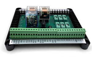
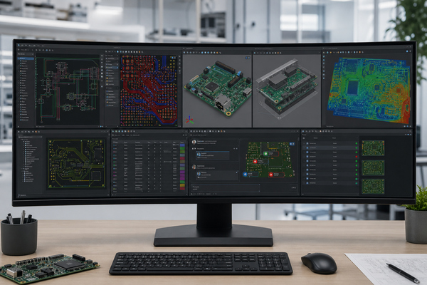
Automotive AMB ceramic PCB fabrication scene with ceramic substrates and power module inspection

In the fabrication flow, the supplier reviews the drawing, ceramic type, copper thickness, conductor pattern, isolation distance, surface finish, edge tolerance, and sample quantity before confirming the route. For automotive projects, the review should also include thermal cycling expectations, partial discharge or dielectric requirements when applicable, and whether the prototype must represent the future production process.

Compared with standard FR4 PCB or metal-core PCB, AMB is usually considered for higher-power sections of the system, not low-power control electronics. It belongs in the same decision space as ceramic PCB, DBC ceramic substrates, and other power electronic substrate technologies.

Why Are AMB Ceramic Substrates Used in Automotive Power Modules?

AMB ceramic substrates are used in automotive power modules because they combine electrical insulation, heat transfer, copper current paths, and stronger copper-to-ceramic bonding for harsh power cycling conditions. This matters most when the module carries IGBT, SiC MOSFET, diode, or power-dense switching components in an EV inverter, DC-DC converter, onboard charger, or motor control unit.

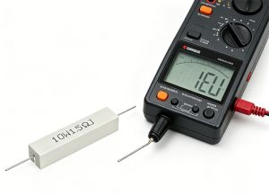
AMB ceramic substrate used inside an automotive power module assembly

The core design logic is stress management. Power devices heat and cool quickly, while copper, ceramic, solder, die attach, and baseplate materials expand differently. If the substrate cannot manage this mismatch, the module may suffer copper delamination, ceramic cracking, solder fatigue, increased thermal resistance, or early electrical failure.

AMB is not necessary for every automotive PCB component. Low-current sensor boards, control boards, lighting controllers, and communication boards may use FR4, high-Tg FR4, rigid-flex, or MCPCB depending on temperature and mechanical requirements. AMB becomes relevant when the circuit carrier is part of the thermal and mechanical reliability path of the power module.

How Does AMB Ceramic Compare with DBC and DPC?

The choice between AMB, DBC, and DPC should start with power density, copper thickness, line resolution, material, and thermal cycling risk. AMB is often considered when mechanical reliability and copper bonding strength matter more than very fine conductor geometry.

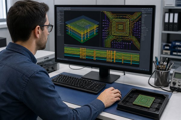
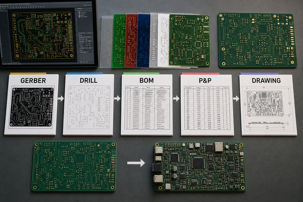
Comparison image showing AMB DBC and DPC ceramic substrate options for power modules
Technology Best fit Buyer should check
AMB ceramic substrate High-reliability power modules, especially with Si3N4 or demanding thermal cycling Brazing quality, copper adhesion, ceramic toughness, voids, and thermal cycling data
DBC / DCB ceramic substrate Mature power module designs that need thick copper and strong heat spreading Ceramic type, copper thickness, etching limits, dielectric strength, and solderability
DPC ceramic PCB Finer conductor patterns, smaller features, or designs needing plated structures Line width, via structure, plating thickness, and whether current capacity is sufficient

If the design combines high current, thick copper, and severe thermal cycling, AMB or DBC should usually be evaluated before DPC. If the design needs finer routing and lower current, DPC may be more practical. For an RFQ, ask the supplier to explain the process recommendation instead of quoting only the requested keyword.

Which Materials Matter in AMB Ceramic PCB Fabrication?

The main materials in AMB ceramic PCB fabrication are the ceramic substrate, copper layer, active brazing material, and final surface finish. For automotive power modules, the ceramic choice can affect thermal conductivity, bending strength, fracture toughness, dielectric behavior, and long-term cycling performance.

AMB ceramic substrate material selection showing Si3N4 AlN and Al2O3 ceramic samples with copper patterns
Material Why buyers consider it Practical caution
Si3N4 Often selected for higher mechanical toughness and thermal cycling resistance in demanding power modules Cost, availability, thickness, and supplier process maturity should be confirmed early
AlN Selected when high thermal conductivity is a primary driver Mechanical robustness and cycling performance must be reviewed with the exact module design
Al2O3 Useful when cost and insulation matter more than maximum thermal performance May not be enough for high-power automotive modules with aggressive heat density

For high-risk automotive applications, do not choose only by thermal conductivity. A substrate with higher thermal conductivity but lower mechanical margin may still create reliability risk if the copper thickness, die attach, baseplate, and thermal cycling profile are not matched.

What Automotive PCB Components Use AMB Ceramic Substrates?

AMB ceramic substrates are mainly used in automotive power electronics components where the circuit carrier is exposed to high heat flux, high current, and repeated load changes. They are less relevant for ordinary logic boards and more relevant for modules that sit close to power semiconductor devices.

  • EV traction inverter power modules using SiC MOSFETs, IGBTs, or diodes.
  • Onboard charger power conversion modules.
  • DC-DC converter modules for high-voltage to low-voltage conversion.
  • Motor control modules and high-load switching units.
  • Battery thermal management or high-current protection circuits when ceramic isolation and heat spreading are needed.

For mixed automotive PCB assemblies, the AMB substrate is often only one part of the full electronic system. The surrounding gate driver, sensing, communication, and control circuits may still use conventional PCB or PCBA processes, so the supplier handoff between ceramic substrate fabrication and assembly review should be planned early.

What Manufacturing Factors Affect AMB Ceramic PCB Quality?

AMB ceramic PCB quality is strongly affected by ceramic preparation, copper thickness, brazing interface quality, pattern etching, surface finish, edge processing, and inspection. A buyer should review these factors before approving a prototype because they influence both electrical performance and long-term mechanical reliability.

  • Copper thickness: affects current carrying capacity, heat spreading, etching geometry, and stress at the copper-to-ceramic interface.
  • Pattern geometry: sharp corners, narrow gaps, large copper islands, and asymmetric copper balance can change stress concentration.
  • Brazing interface: voids, poor wetting, or inconsistent bonding can increase thermal resistance and reduce cycling life.
  • Ceramic edge quality: chips, microcracks, and rough edges can create handling and reliability risk.
  • Surface finish: should match die attach, soldering, wire bonding, or module assembly requirements.

EBest Circuit (Best Technology) lists AMB ceramic PCB among its ceramic PCB technology scope, together with DPC, DBC/DCB, LTCC, HTCC, thick-film, and thin-film ceramic PCB. For automotive use, any maximum capability or fast-turn request should still be checked against material, dimensions, copper thickness, testing scope, and engineering review.

What Reliability Tests Matter for Automotive AMB Ceramic PCB?

Reliability testing for automotive AMB ceramic PCB should focus on thermal cycling, power cycling relevance, insulation, copper adhesion, dimensional stability, solderability, and visual or microstructural inspection. The exact test plan should match the module’s voltage class, mission profile, assembly method, and customer qualification standard.

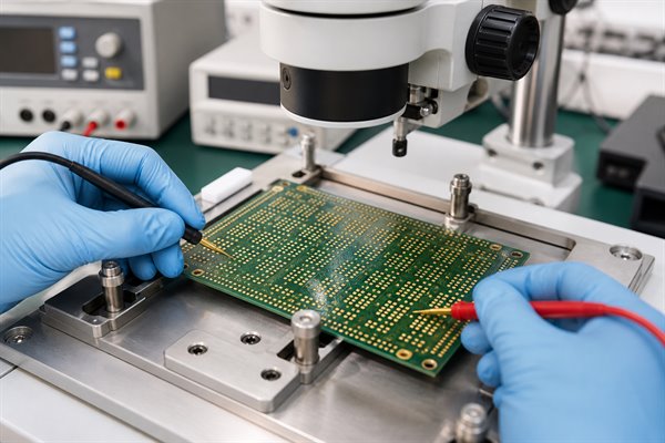
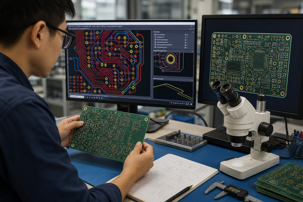
Automotive AMB ceramic PCB reliability testing with thermal cycling inspection and electrical test equipment
Check Why it matters Buyer action
Thermal cycling Finds stress-related issues at the copper, braze, ceramic, and solder interfaces Share the expected temperature range and cycle target before quoting
Dielectric / insulation testing Confirms isolation margin for high-voltage automotive modules Specify voltage, spacing, and acceptance criteria
Microsection or interface review Helps evaluate voids, bonding quality, copper thickness, and process consistency Request sample inspection data for critical prototype builds
Dimensional inspection Protects module fit, die placement, and baseplate alignment Mark critical dimensions separately from non-critical dimensions

For SiC traction inverter modules, power cycling is especially relevant because it stresses the package under realistic electrical and thermal load changes. Even when the AMB supplier does not run full module-level power cycling, the substrate design should be reviewed with that stress path in mind.

What Should Buyers Provide for an AMB Ceramic PCB Quote?

A useful AMB ceramic PCB quote requires more than Gerber files. The supplier needs enough design and application context to judge material fit, copper thickness, brazing route, test requirements, and whether the prototype can scale to automotive production.

  • Gerber, drill, drawing, and copper layer data.
  • Ceramic material preference, such as Si3N4, AlN, or Al2O3.
  • Copper thickness, substrate thickness, and finished board thickness.
  • Surface finish and assembly method, including soldering, die attach, or wire bonding needs.
  • Voltage, current, insulation distance, and thermal load targets.
  • Critical dimensions, tolerance class, and edge quality requirements.
  • Prototype quantity, expected production volume, and PPAP or automotive documentation expectations.
  • Required inspection reports, thermal cycling requirements, and packaging instructions.

If the project includes assembled automotive PCB components, send BOM, placement data, thermal interface notes, and test requirements at the same time. This lets the supplier check substrate fabrication and downstream assembly risks together instead of discovering mismatches after samples are made.

How to Choose Automotive PCB Suppliers for AMB Ceramic Projects?

Automotive PCB suppliers for AMB ceramic projects should be evaluated by engineering review quality, ceramic substrate experience, inspection capability, documentation discipline, and ability to support prototype-to-production transfer. A supplier that can quote quickly but cannot explain material trade-offs may create risk during qualification.

Ask each supplier how they review Si3N4 versus AlN, which copper thicknesses fit the selected process, what inspection data can be provided for prototypes, how they control edge damage, and what information is needed before mass production. If automotive documentation is required, confirm expectations before the prototype order, not after the design is frozen.

EBest Circuit (Best Technology) can be positioned as a ceramic PCB and PCBA manufacturing partner for buyers who need engineering communication across prototype review, ceramic substrate fabrication, assembly discussion, and quotation preparation. For AMB projects, the useful conversation is not a generic price request; it is a file-and-requirement review that connects material choice, reliability target, and production feasibility.

FAQ

What is AMB ceramic PCB fabrication used for in automotive electronics?

AMB ceramic PCB fabrication is used for high-power automotive electronics where the substrate must provide insulation, heat spreading, copper current paths, and thermal cycling resistance. Typical uses include EV inverter power modules, onboard chargers, DC-DC converters, motor control modules, and other circuits that place SiC MOSFETs, IGBTs, or diodes close to the heat path.

Is AMB ceramic better than DBC for automotive power modules?

AMB is not automatically better than DBC; it is better suited when the design needs stronger copper-to-ceramic bonding and improved mechanical reliability under severe thermal cycling. DBC remains a mature option for many power modules. The correct choice depends on ceramic material, copper thickness, module stress profile, cost target, and qualification requirements.

Which ceramic material is best for AMB power modules?

Si3N4 is often considered for demanding AMB power modules because it offers strong mechanical toughness and thermal cycling resistance. AlN is attractive when thermal conductivity is the main driver, while Al2O3 is more cost-oriented but usually less suitable for high-power automotive modules. Buyers should review material choice with copper thickness, module layout, and test requirements together.

What files are needed for an automotive AMB ceramic PCB quote?

A useful quote should include Gerber data, mechanical drawings, ceramic material preference, copper thickness, substrate thickness, surface finish, voltage and current targets, thermal load, critical tolerances, sample quantity, production estimate, and reliability test expectations. If assembly is involved, include BOM, placement data, die attach or soldering notes, and packaging requirements.

Can AMB ceramic substrates be assembled into automotive power modules?

Yes, AMB ceramic substrates can be used in automotive power module assembly, but the assembly method must be reviewed early. Die attach, solderability, wire bonding, surface finish, baseplate attachment, insulation spacing, and thermal interface materials can all affect reliability. The substrate supplier and assembly team should align before prototype approval.

How should buyers evaluate automotive PCB suppliers for AMB ceramic projects?

Buyers should evaluate whether the supplier can review ceramic material, copper thickness, AMB process route, edge quality, inspection data, thermal cycling expectations, and prototype-to-production transfer. For automotive projects, also check documentation discipline, traceability expectations, quality system fit, and whether the supplier can explain trade-offs instead of only quoting a price.

Conclusion

Automotive AMB ceramic PCB fabrication is most useful when the design needs a ceramic power substrate for high current, heat spreading, insulation, and thermal cycling reliability. It is not the default choice for every automotive PCB; it should be selected when the power module’s stress profile, device type, copper requirement, and qualification plan justify the process.

Before requesting a quote, prepare the material target, copper thickness, drawings, electrical and thermal requirements, prototype quantity, expected production volume, and reliability test expectations. If you are evaluating AMB ceramic substrates for automotive power modules, contact EBest Circuit (Best Technology) at sales@bestpcbs.com for engineering review and quotation support.

You may also like

Custom PCB Design for Teleoperation: Latency, Power and RF Checks

July 13th, 2026
Custom PCB design for teleoperation robot controller with remote control and lab test equipment

Custom PCB design for teleoperation should protect the remote-control link, motor-control power path, sensor feedback, test access and enclosure interface before the first prototype is ordered. A teleoperation PCB is not just a robot controller board. It carries the electronics that help an operator send commands, receive feedback and keep the machine predictable when wireless quality, vibration, load current or cable routing changes.

This guide is written for engineers and buyers preparing a custom PCB or PCBA for teleoperated robots, remote inspection equipment, mobile platforms, industrial manipulators, UAV ground systems, field-service devices or hazardous-area remote tools. It focuses on manufacturable PCB checks and RFQ readiness, not on robot-control algorithms.

What does custom PCB design for teleoperation need to control?

A teleoperation PCB needs to keep command input, feedback data, power conversion, motor drivers, sensors and safety-related I/O electrically separated enough to avoid unstable behavior. The design may include a microcontroller or processor, RF or wired communication module, camera or sensor inputs, encoder lines, motor-driver interfaces, battery or DC input, protection circuits and connectors to the robot body.

The board should be reviewed as a system. A clean schematic can still fail in the field if motor-current return paths disturb the receiver, if a camera interface sits beside a noisy regulator, or if a connector harness pulls against a weak solder joint. When wireless range, antenna routing or controlled impedance matters, compare the design against an RF PCB capability early instead of treating the radio section as a normal digital trace group.

Teleoperation PCB area Design check Why it matters
Communication link Antenna clearance, controlled routing, shielding, connector loss and RF module placement Weak links create command delay, dropouts or unstable feedback
Power input Battery/DC range, transient protection, regulator heat and local decoupling Remote machines often see load surges and cable voltage drop
Motor and actuator paths High-current loops, driver heat, return path and separation from sensors Motor noise can reset logic or corrupt feedback signals
Sensor feedback Encoder, camera, IMU, limit switch and telemetry routing The operator needs reliable state information, not only command output
Production test Programming access, test pads, fixture clearance and functional-test limits A prototype that cannot be tested repeatably is not ready for volume

How should latency and link reliability affect PCB layout?

PCB layout cannot remove all network delay, but it can reduce board-level causes of packet loss, noise coupling and unreliable command response. Teleoperation systems are sensitive to latency, jitter and communication dropouts, so the board should not add avoidable RF, grounding or power noise problems on top of the software and network layer.

Keep the antenna or RF module away from motor drivers, switching regulators, displays, dense cable bundles and metal enclosure walls unless the RF design intentionally accounts for them. Follow the module vendor’s keep-out and ground rules. If the design uses external antennas, review connector type, cable routing, mounting torque and enclosure feedthrough. If it uses wired control, check differential-pair routing, shielding, ESD protection and connector strain relief.

Teleoperation PCB signal validation with oscilloscope, RF cables and remote-control hardware
Teleoperation PCBs should be validated around command signals, feedback data and RF or wired communication paths.

Do not bury the communication decision inside a generic PCB order. If the board includes RF, Ethernet, CAN, RS-485, USB, camera links or high-speed sensor data, the stackup, reference planes and connector placement should be part of the RFQ review. Related control-network design checks are also covered in the custom PCB design for industrial networks guide.

What power architecture should a remote robot controller use?

The power architecture should separate noisy actuator energy from logic, RF, sensors and safety I/O while still sharing a controlled grounding strategy. Teleoperated equipment often combines battery packs, DC input, motor drivers, servos, radios, cameras, lamps, heaters or brakes. Those loads should not all be treated as a single quiet supply problem.

Start by listing each rail, load current, startup sequence, allowable voltage range and heat source. Use local decoupling for processors, RF modules and sensors. Keep high-current switching loops short. Give motor-driver current a planned return path instead of letting it travel under the communication and sensor sections. If the design has high-current power electronics, heavier copper, thermal vias, wider pours or separate power boards may be needed; do not infer current capacity from trace width alone without reviewing temperature rise and board stackup.

How should motor noise, sensors and safety I/O be isolated?

Motor-control noise should be handled with placement, return-path control, filtering, connector separation and test access before the PCB is released. Teleoperation failures are often blamed on software, but random resets, lost encoder counts, noisy video, false limit-switch signals and unstable IMU readings can come from board-level coupling.

Place motor drivers and power switching away from sensitive analog, RF and feedback circuits. Use clear zones for encoder inputs, current sensing, limit switches, emergency-stop inputs and feedback buses. Add test points for rails, reset lines, communication status, actuator enable lines and critical sensors. For first builds, treat the project as a Prototype PCB Assembly job so assembly feedback, component alternates and functional-test access can be corrected before production.

Which PCB materials and stackups fit teleoperation boards?

Most teleoperation controller boards can start with FR4, but RF, high-speed, thermal, vibration and enclosure constraints may require stackup changes. A simple two-layer board may work for low-speed prototypes. A production controller with RF, cameras, processors, motor drivers and many connectors usually benefits from four or more layers because planes improve return paths, noise control and routing density.

Use high-frequency laminates or hybrid stackups only when the RF section, bandwidth or antenna design justifies the cost. For compact mobile equipment, board outline, connector height, stiffeners and mounting holes can be as important as material choice. If a remote unit needs a folded sensor harness, moving camera module or tight enclosure path, review whether flex or rigid-flex is more reliable than multiple cable connectors.

What should be checked before PCBA production?

Before PCBA production, verify that the board can be assembled, programmed, calibrated, inspected and tested under realistic command and load conditions. A teleoperation controller should not rely only on visual inspection or continuity testing. It needs checks that match how the remote machine behaves.

Teleoperation controller PCBA inspection with connector harness test fixture and assembled control boards
Connector, harness and functional-test planning should be part of the teleoperation PCBA build package.

Define programming access, bootloader method, firmware version control, fixture pins, current-limit settings, communication checks and pass/fail criteria. Test the board with expected cable lengths, antenna placement and representative actuator loads when possible. Supplier-side PCB test equipment should be discussed before volume builds if the project needs fixture-based functional testing, not after the pilot run exposes missing pads.

How should connectors, harnesses and enclosures be planned?

Connectors and harnesses should be placed around assembly access, strain relief, service direction, cable noise and enclosure sealing. Teleoperated products often fail mechanically before they fail electrically: vibration loosens cables, operator ports get stressed, or enclosure walls block connector access.

Check connector locking style, mating cycles, wire gauge, cable bend radius, shield termination, gasket clearance and mounting screw access. Keep high-current motor wiring away from RF and sensor lines where possible. If the supplier is expected to deliver a tested controller inside a housing, discuss Box Build Assembly requirements such as harness routing, enclosure labels, final test and packing constraints.

RFQ checklist for custom teleoperation PCB design

A useful RFQ package should show the supplier the control architecture, RF or wired link, power budget, motor loads, enclosure constraints and test requirements. Without those details, the quote may cover board fabrication but miss the risks that make a teleoperation product hard to build.

  1. Gerber files, drill files, netlist, stackup, copper weight and controlled revision number.
  2. Schematic, BOM, approved alternates, centroid file and assembly drawing.
  3. Communication method: RF module, antenna type, Ethernet, CAN, RS-485, USB, camera link or mixed interfaces.
  4. Power input range, battery or DC supply notes, maximum load current and motor-driver information.
  5. Connector drawings, harness direction, enclosure model, mounting holes and height limits.
  6. Programming method, firmware loading requirement and board-level functional-test criteria.
  7. Environmental notes such as vibration, dust, humidity, outdoor use, heat, chemical exposure or service access.
  8. Any components that require sourcing approval, lifecycle review or controlled substitutes.

Teleoperation products often depend on RF modules, processors, connectors, motor drivers, sensors and power ICs that cannot be swapped casually. Involve Component Sourcing before the pilot build if approved alternates, lifecycle status or lead-time risk could change the control behavior.

Supplier questions buyers should ask

Supplier questions should force a real engineering review of link reliability, power integrity, assembly risk and test coverage. A low unit price is not useful if the first build cannot be programmed, calibrated or tested under load.

  • Which layout areas are most likely to affect RF range, command response or feedback quality?
  • Are the antenna, connector and enclosure positions compatible with the communication method?
  • Do motor-driver current paths stay away from logic, RF and sensor feedback?
  • Are all programming, debug and functional-test pads reachable after assembly?
  • Which parts need approved alternates before production?
  • Can the test fixture simulate command input, feedback output and representative load current?
  • What should change before moving from engineering prototype to pilot production?

FAQ

What is custom PCB design for teleoperation?

Custom PCB design for teleoperation means designing a circuit board for remote command input, machine feedback, communication, power conversion, motor control, sensors and production test. The board must support predictable remote operation, not only basic robot movement.

Does teleoperation always need an RF PCB?

No. Some systems use wired Ethernet, CAN, RS-485 or tethered control. RF PCB review becomes important when the board includes antennas, wireless modules, controlled-impedance traces, coax connectors or tight enclosure constraints that affect radio performance.

What causes unstable teleoperation controller behavior?

Common board-level causes include motor noise coupling into logic, weak power rails, poor grounding, antenna placement problems, cable shielding mistakes, missing ESD protection, inaccessible test pads and firmware loading issues. Network software can also matter, but the PCB should not add preventable electrical faults.

How many layers should a teleoperation controller PCB use?

Simple prototypes may use two layers, but four or more layers are often safer when the board has RF, processors, motor drivers, cameras, sensors and many connectors. Planes help control return paths, EMI, routing density and power integrity.

What files are needed for a teleoperation PCB quote?

Send Gerber and drill files, schematic, BOM, centroid file, assembly drawing, stackup, enclosure notes, communication method, power budget, connector drawings and test requirements. Include firmware-loading and functional-test notes if the supplier will assemble the PCBA.

Conclusion

Custom PCB design for teleoperation should be reviewed around the full control path: command link, RF or wired interface, power rails, motor noise, sensor feedback, connectors, enclosure and test access. A supplier can quote more accurately when the RFQ includes the board files plus communication, power, harness and functional-test requirements. For a remote-control product, that preparation is often the difference between a board that only powers up and a controller that can be built, tested and improved repeatably.

You may also like

What Is Tachyon 100G? Ultra-Low-Loss High-Speed PCB Laminate & Prepreg

July 13th, 2026

Tachyon 100G is an ultra-low-loss laminate and prepreg system for very high-speed digital PCB applications. It supports data rates of 100 Gb/s and beyond. Its Dk of 3.02, Df of 0.0021, Tg of 215°C and Td of 360°C help control signal loss and thermal stress.

The material is mainly used in dense multilayer PCBs, long high-speed channels and fine-pitch BGA designs. However, laminate selection alone does not guarantee channel performance. Copper profile, prepreg, stackup geometry and via structure must also be controlled.

Tachyon 100G, https://www.bestpcbs.com/blog/2026/07/tachyon-100g/

What Is Tachyon 100G?

Tachyon 100G is an Isola ultra-low-loss laminate and prepreg material for very high-speed digital PCB designs. It is intended for data rates of 100 Gb/s and beyond. The material is recognized under IPC-4103/17 and IPC-4101/102 and is RoHS compliant.

The standard laminate offering covers 2 to 20 mil, or 0.05 to 0.51 mm. Listed copper weights include 0.5 oz, 1 oz and 2 oz. Thinner and heavier copper foil can also be available.

Unlike standard FR-4, this laminate system focuses on loss control and stable electrical behavior. Low Dk glass, square weave glass and mechanically spread glass are available. Low-profile copper options also help reduce conductor loss.

As a result, this high-speed PCB material is a strong fit for backplanes, daughter cards and line cards. It is most useful when insertion loss and timing margin directly affect channel performance.

Why Is Tachyon 100G Suitable for Ultra-Low-Loss High-Speed PCBs?

The material combines low dielectric loss, stable electrical properties and low-profile copper options. Its electrical behavior remains stable from -55°C to +125°C and at frequencies up to 100 GHz.

Its main advantages include:

  • Low dielectric loss: A typical Df of 0.0021 limits dielectric loss as frequency rises.
  • Stable Dk: A Dk of 3.02 at 5 GHz and 10 GHz supports predictable impedance design.
  • Spread glass options: Spread glass helps reduce local dielectric variation and differential skew.
  • Low-profile copper: HVLP3, HVLP and Advanced RTF options reduce roughness-related conductor loss.
  • Low Z-axis expansion: A pre-Tg Z-axis CTE of 45 ppm/°C supports plated-hole reliability.
  • Strong thermal capability: The material supports six 260°C reflow cycles and six 288°C solder-float exposures.
  • HDI compatibility: Multiple lamination cycles and HDI processing are listed as material advantages.

In practice, these properties help improve eye opening and reduce jitter in loss-sensitive digital channels. They do not correct poor routing, plane splits or long via stubs. The PCB design must still protect the complete signal path.

What Is the Dielectric Constant of Tachyon 100G?

The typical dielectric constant is 3.04 at 2 GHz and 3.02 at both 5 GHz and 10 GHz. The datasheet also lists a typical Df of 0.0021 across the stated 2–10 GHz values.

FrequencyDkDf
2 GHz3.040.0021
5 GHz3.020.0021
10 GHz3.020.0021

These values support controlled-impedance design and high-speed channel modeling. However, 3.02 should not be used as one universal value for every dielectric layer.

Glass style, resin content and pressed dielectric thickness can change the effective dielectric behavior. The exact laminate and prepreg construction should be confirmed before final routing.

For production, calculate impedance from the released stackup. Then verify the finished PCB with impedance coupons and actual manufacturing geometry.

What Is the CTE Value of Tachyon 100G Material?

The Z-axis CTE is 45 ppm/°C below Tg and 250 ppm/°C above Tg. Total Z-axis expansion from 50°C to 260°C is 2.5%. The X/Y-axis CTE below Tg is 15 ppm/°C.

DirectionConditionCTE
Z-axisPre-Tg45 ppm/°C
Z-axisPost-Tg250 ppm/°C
Z-axis50–260°C2.5%
X/Y-axisPre-Tg15 ppm/°C

Z-axis expansion matters during lamination, reflow and thermal cycling. Excessive expansion increases stress around plated through holes and internal copper connections.

Tachyon 100G thermal performance is especially relevant to high-layer-count PCBs and fine-pitch BGA structures. Even so, CTE must be reviewed with board thickness, via aspect ratio and total thermal exposure.

A high-performance material cannot compensate for poor drilling or weak hole-wall plating. Material behavior and PCB process control must be evaluated together.

Isola Tachyon 100G Material Properties & Datasheet Overview

The June 23, 2026 Revision H datasheet lists Tg 215°C, Td 360°C, Dk 3.02 and Df 0.0021 as headline values. Revision H also corrects the Df test method and provides detailed thermal, electrical and mechanical data.

Thermal and Electrical Properties

PropertyTypical ValueTest Method
Tg, DSC215°CIPC-TM-650 2.4.25C
Tg, DMA230°CIPC-TM-650 2.4.24.4
Tg, TMA210°CIPC-TM-650 2.4.24C
Td, 5% Weight Loss360°CIPC-TM-650 2.4.24.6
T260>60 minIPC-TM-650 2.4.24.1
T288>60 minIPC-TM-650 2.4.24.1
T300>20 minIPC-TM-650 2.4.24.1
Z-CTE, Pre-Tg45 ppm/°CIPC-TM-650 2.4.24C
Z-CTE, Post-Tg250 ppm/°CIPC-TM-650 2.4.24C
Z Expansion, 50–260°C2.5%IPC-TM-650 2.4.24C
X/Y CTE, Pre-Tg15 ppm/°CIPC-TM-650 2.4.24C
Thermal Conductivity0.42 W/m·KASTM E1952
Thermal StressPassIPC-TM-650 2.4.13.1
Dk, 2 GHz3.04IPC-TM-650 2.5.5.5
Dk, 5 GHz3.02IPC-TM-650 2.5.5.5
Dk, 10 GHz3.02IPC-TM-650 2.5.5.5
Df, 2–10 GHz0.0021Bereskin Stripline
Volume Resistivity1.33 × 10⁷ MΩ-cmIPC-TM-650 2.5.17.1
Surface Resistivity1.33 × 10⁵ MΩIPC-TM-650 2.5.17.1
Dielectric Breakdown60 kVIPC-TM-650 2.5.6B
Arc Resistance125 secIPC-TM-650 2.5.1B
Electric Strength60 kV/mmIPC-TM-650 2.5.6.2A

Mechanical and Safety Properties

PropertyTypical ValueTest Method
CTIClass 3, 175–249 VUL 746A / ASTM D3638
Peel Strength0.79 N/mmIPC-TM-650 2.4.8C
Peel Strength After Stress0.96 N/mmIPC-TM-650 2.4.8.2A
Flexural Strength, Length303 MPaIPC-TM-650 2.4.4B
Flexural Strength, Cross283 MPaIPC-TM-650 2.4.4B
Tensile Strength, Length207 MPaASTM D3039
Tensile Strength, Cross172 MPaASTM D3039
Young’s Modulus, Length2,551 ksiASTM D790-15e2
Young’s Modulus, Cross2,417 ksiASTM D790-15e2
Taylor’s Modulus, Length2,264 ksiASTM D790-15e2
Taylor’s Modulus, Cross2,197 ksiASTM D790-15e2
Poisson’s Ratio, Length0.165ASTM D3039
Poisson’s Ratio, Cross0.156ASTM D3039
Moisture Absorption0.1%IPC-TM-650 2.6.2.1A
FlammabilityV-0UL 94
RTI130°CUL 746

The Tachyon 100G thermal conductivity is 0.42 W/m·K. This is a laminate value, not a complete PCB thermal solution.

Copper planes, thermal vias, component power density and airflow still control board-level heat transfer. The datasheet also lists 0.1% moisture absorption, UL 94 V-0 and an RTI of 130°C.

The combined data show strong electrical and thermal capability. They also support complex multilayer PCB structures and repeated thermal processing.

What Thickness Options Are Available for Tachyon 100G Prepreg?

The datasheet does not publish one fixed thickness range for Tachyon 100G prepreg. The listed 2 to 20 mil range applies to laminate, not prepreg.

Available prepreg fabric options include low Dk glass, square weave glass and mechanically spread glass. Final dielectric thickness depends on glass construction, resin content, ply count and lamination press-out.

Therefore, select the prepreg by finished dielectric spacing and target impedance. Confirm the actual construction before releasing the PCB stackup for production.

How Should a Tachyon 100G PCB Stackup Be Designed for High-Speed Signals?

A Tachyon 100G PCB stackup should be built around channel loss, controlled impedance and continuous return paths. The material construction should be confirmed before final high-speed routing.

  • Place high-speed signal layers beside continuous GND planes. SerDes and differential pairs require a stable return path. Avoid plane splits, large voids and reference changes beneath critical traces.
  • Use the selected dielectric construction for impedance calculation. Do not apply Dk 3.02 to every layer without checking the actual buildup. Core, prepreg, glass construction and resin content can affect dielectric behavior.
  • Control finished dielectric thickness. Trace width and spacing should be calculated from the pressed dielectric target. Prepreg nominal construction alone does not define the finished layer spacing.
  • Use low-profile copper on loss-critical layers. HVLP3 is listed at ≤1.1 µm Rz JIS. HVLP and Advanced RTF are listed at ≤2.5 µm Rz JIS.
  • Keep high-speed routes short and direct. Reduce unnecessary meanders and excessive layer transitions. Longer traces increase dielectric and conductor loss.
  • Minimize signal via stubs. Review through-hole via length during channel simulation. Use back drilling when the remaining stub causes unacceptable resonance or return loss.
  • Optimize anti-pad geometry. Via barrel, pad and anti-pad dimensions should be modeled together. Poor anti-pad design can create a large impedance discontinuity.
  • Provide a return path at every layer transition. Place GND stitching vias close to signal vias. This gives return current a short path between reference planes.
  • Control differential-pair geometry. Maintain the designed trace width, spacing and reference-plane distance. Avoid uncontrolled neck-down sections around BGA fanout and connectors.
  • Review fiber-weave interaction. Spread-glass options help reduce local dielectric variation. Long differential pairs should still be reviewed for skew.
  • Keep the layer buildup symmetrical. Balance dielectric thickness and copper distribution around the board centerline. This reduces bow, twist and lamination stress.
  • Review copper distribution before lamination. Large copper-density differences can affect resin flow and pressed dielectric thickness. Copper balancing should be included in the manufacturing review.
  • Plan BGA breakout before locking the stackup. Fine-pitch fanout can change via type, layer count and reference-plane continuity.
  • Define controlled-impedance requirements in the fabrication data. Include target values, tolerances and trace layers. Suitable impedance coupons should be included for measurement.
  • Verify the finished PCB. Impedance testing confirms the production geometry. Loss-sensitive projects may also require insertion-loss or channel-level validation.

The laminate, copper profile, via structure and return path must be designed as one high-speed channel. A Tachyon 100G PCB cannot deliver its expected performance with an uncontrolled stackup.

Tachyon 100G PCB Stackup, https://www.bestpcbs.com/blog/2026/07/tachyon-100g/

Tachyon 100G vs Megtron 6: Which Material Should You Choose?

For a numerical comparison, the exact MEGTRON 6 grade must be identified. The table below uses Panasonic MEGTRON 6 R-5775 as the comparison baseline.

PropertyTachyon 100GMEGTRON 6 R-5775
Dk3.02 @ 10 GHz3.61 @ 10 GHz
Df0.00210.004 @ 10 GHz
Tg, DSC215°C185°C
Tg, DMA230°C210°C
Td360°C410°C
T288>60 min>120 min
Z-CTE, Pre-Tg45 ppm/°C45 ppm/°C
Z-CTE, Post-Tg250 ppm/°C260 ppm/°C
X/Y CTE, Pre-Tg15 ppm/°C14–16 ppm/°C
Moisture Absorption0.1%0.14%
Peel Strength0.79 N/mm0.8 kN/m
FlammabilityUL 94 V-0UL 94 V-0

Choose Tachyon 100G when dielectric loss and low nominal Dk are the main channel limits. Its published Df of 0.0021 is lower than the 0.004 value listed for R-5775 at 10 GHz.

MEGTRON 6 R-5775 shows stronger published Td and T288 values. It lists Td 410°C and T288 above 120 minutes. Tachyon 100G lists Td 360°C and T288 above 60 minutes.

For Z-axis expansion, the two materials are close. Both list 45 ppm/°C below Tg. The post-Tg values are 250 ppm/°C and 260 ppm/°C, respectively.

However, Dk and Df values should be reviewed with the test method and exact material construction. Published datasheet values support initial selection but do not replace channel simulation.

For long, loss-limited channels, Tachyon 100G has the stronger published dielectric-loss position. For an established MEGTRON 6 platform, qualification history and revalidation cost may justify retaining the approved material.

Where Is Tachyon 100G Commonly Used?

Tachyon 100G is mainly used where long channels and dense multilayer structures create signal-loss or thermal challenges. The material is common in networking, communications, computing, storage, aerospace and defense electronics.

Typical applications include:

  • High-speed network backplanes
  • Switch and router line cards
  • Server PCB assemblies
  • Data center hardware
  • High-speed daughter cards
  • Computing and storage systems
  • High-layer-count communication PCBs
  • Fine-pitch BGA PCB designs
  • Aerospace electronic systems
  • Defense communication electronics

A 100G interface does not automatically require this laminate. Channel length, connectors, via topology and copper roughness can change the loss budget.

For example, a short channel may have enough margin with another qualified low-loss material. A longer path with several transitions may benefit more from the ultra-low-loss dielectric system.

Select the material from the channel and reliability requirements, not from the product name alone.

What Affects Tachyon 100G PCB Cost?

Tachyon 100G PCB cost depends on material construction and manufacturing complexity. There is no fixed material or PCB price for every project.

The main cost factors include:

  • Laminate construction: Core thickness and panel usage affect material cost.
  • Prepreg selection: Glass construction, ply count and dielectric spacing change the multilayer buildup.
  • Copper foil type: HVLP3, HVLP and Advanced RTF can change material sourcing.
  • Copper weight: Standard listed options include 0.5 oz, 1 oz and 2 oz.
  • Layer count: More layers increase laminate, prepreg, imaging and lamination work.
  • Sequential lamination: Complex HDI structures add extra production stages.
  • Drilling complexity: Small holes and thick boards increase drilling and plating control.
  • Back drilling: Stub removal adds depth control and verification.
  • Controlled impedance: Tight tolerances and coupon testing increase process control.
  • Order quantity: Prototype and volume panel utilization are different.

The first cost-control step is to define the real channel-loss target. Do not use the highest-cost construction on every layer without a technical reason.

For procurement, lock the released stackup before requesting volume pricing. This makes PCB supplier quotations easier to compare and reduces later material changes.

Why Choose EBest Circuit as Your Tachyon-100G PCB Manufacturer?

Choosing the correct laminate is only the first step. EBest Circuit helps reduce stackup, material and production risks before volume manufacturing.

  • Reduce stackup changes after layout release. We review laminate, prepreg, copper weight and dielectric spacing before production.
  • Protect controlled-impedance performance. Trace layers, impedance targets and manufacturing geometry are reviewed together.
  • Reduce material substitution risk. Specified laminate and copper-profile requirements can be identified before material release.
  • Improve high-layer-count PCB manufacturability. Copper balance, drilling, lamination and board thickness are reviewed before production.
  • Support loss-sensitive via structures. Back drilling, via stubs and high-aspect-ratio holes can be reviewed against the PCB structure.
  • Maintain repeat-order consistency. Material and production information can be controlled for recurring and volume orders.
  • Simplify PCB and PCBA sourcing. PCB fabrication, component sourcing, assembly and testing can be coordinated through one workflow.
  • Match quality control to the project. AOI, electrical testing, impedance testing and microsection inspection can be applied as specified.
  • Support regulated industry programs. EBest Circuit operates with ISO 9001, IATF 16949, ISO 13485 and AS9100D quality system capabilities.
  • Buy directly from a China-based source manufacturer. Custom, prototype and volume PCB programs are manufactured in China and supplied worldwide.

The goal is to make your Tachyon 100G PCB stackup manufacturable, repeatable and ready for volume production.

Tachyon 100G PCB, https://www.bestpcbs.com/blog/2026/07/tachyon-100g/

FAQs About Tachyon 100G PCB Material

Q1: How should Tachyon 100G prepreg be stored before lamination?

A1: Store prepreg at 23°C or below and under 50% relative humidity. Keep it in the original packaging until use. FIFO inventory control also helps reduce moisture-related changes in resin flow and cure behavior.

Q2: Should opened Tachyon 100G prepreg be vacuum sealed?

A2: No. Remaining prepreg should be resealed with fresh desiccant and should not be vacuum sealed. Opened material should be used as soon as practical and protected from uncontrolled humidity.

Q3: What are the suggested starting lamination parameters?

A3: General starting parameters include 200°C cure temperature, 60 minutes at 200°C and a 3–5°C/min heat ramp. Product temperature should remain below 210°C. Final settings must match the actual multilayer construction.

Q4: Does a thick Tachyon 100G PCB require different drilling control?

A4: Yes. Boards above 2.5 mm with high layer counts may require a lower stack height and more conservative drilling parameters. Board thickness, copper structure and hole diameter should be reviewed before setting the drill program.

Q5: How many drill hits are recommended?

A5: A common processing guideline is a maximum of 1,000 hits for drills below 0.020 inch. Drills at or above 0.020 inch may reach 1,500 hits. Actual limits can be lower for thick or difficult PCB structures.

Q6: Does Tachyon 100G require plasma desmear?

A6: Not always. The material responds to chemical desmear. Plasma may help on thick or high-aspect-ratio PCBs where stronger hole-wall preparation is required before copper plating.

Q7: Is two-pass chemical desmear useful for thick boards?

A7: Two chemical-desmear passes may be considered for high-reliability PCBs or boards thicker than 2.5 mm. The exact process should be verified through hole-wall inspection and microsection analysis.

Q8: Can standard aqueous dry film be used for inner-layer imaging?

A8: Yes. Standard aqueous dry film can be used for inner-layer imaging. The material is also compatible with common cupric chloride and ammoniacal etching processes used in multilayer PCB fabrication.

Q9: Should panel flash be sheared after lamination?

A9: Routing is preferred instead of shearing. Removing panel flash by routing can reduce edge crazing risk after multilayer lamination and helps maintain cleaner panel edges before later fabrication processes.

Q10: Why is inner-layer dimensional movement important?

A10: Inner layers can change dimension after etching, oxide treatment and lamination. Artwork compensation should be based on measured production movement. Construction and grain orientation should remain controlled between repeat batches.

Q11: How should finished PCBs be packaged for long storage?

A11: Use a moisture barrier bag, humidity indicator card and suitable desiccant for long storage or high-temperature assembly programs. Finished PCBs should be dry before packaging.

Q12: How long should boards be used after opening the moisture barrier bag?

A12: A processing window of 168 hours is recommended when shop-floor conditions remain below 30°C and 60% RH. Bags opened only for inspection should be resealed promptly.

Tachyon 100G is built for PCB designs where channel loss, impedance stability and high-layer-count reliability directly affect product performance. The right laminate must be matched with the correct prepreg, copper profile, via structure and production stackup.

Do not wait until fabrication to discover that the released stackup is difficult to build or no longer meets the channel target. Send your Gerber or ODB++ files, stackup and impedance requirements to sales@bestpcbs.com. EBest Circuit will review your Tachyon 100G PCB project and provide a manufacturing quotation for prototype or volume production.

You may also like

Is Copper a Good Conductor of Heat?

July 13th, 2026

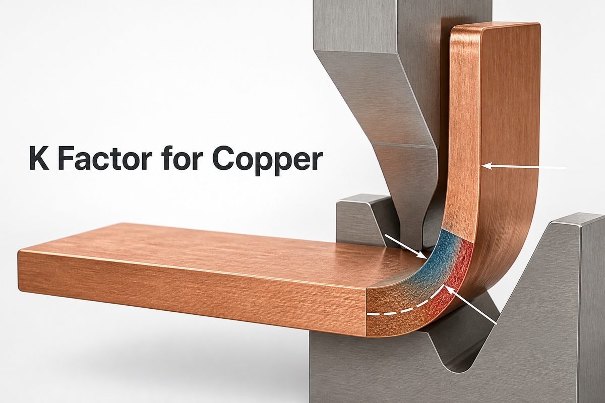
Is Copper a Good Conductor of Heat? Yes, copper is a good conductor of heat. In fact, copper is one of the best common engineering metals for heat conduction. It transfers heat quickly because its atomic structure allows free electrons to move energy through the material efficiently. This is why copper is widely used in heat sinks, heat spreaders, electrical wiring, busbars, power electronics, thermal pads, and PCB designs that need better heat dissipation.

For EBest Circuit (Best Technology), the thermal conductivity of copper is not only a physics concept. It is directly related to PCB manufacturing, copper thickness selection, metal core PCB design, thermal vias, high-power LED boards, power modules, ceramic PCBs, and long-term PCBA reliability. If you are developing a PCB or PCBA project where heat must be controlled, pls feel free to send your Gerber files, stackup, copper thickness, power requirements, or thermal questions to sales@bestpcbs.com. Our engineering team can help review the manufacturing path before production starts.

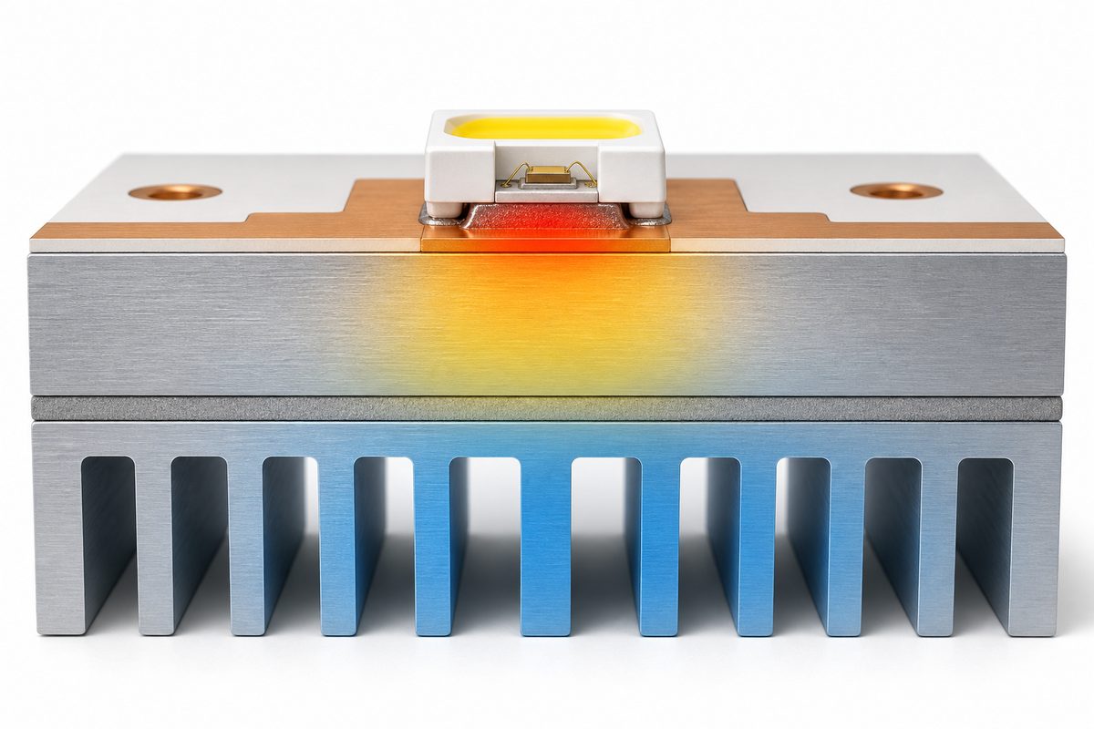
Is Copper a Good Conductor of Heat

Is Copper a Good Conductor of Heat?

Copper is a very good conductor of heat. Pure copper has a thermal conductivity of roughly 390 to 400 W/m·K at room temperature, depending on purity and measurement conditions. This is much higher than many common metals and far higher than most plastics, glass, ceramics, FR4 laminate, and air.

In simple terms, copper can move heat away from a hot area quickly. If one side of a copper part is heated, the heat spreads through the copper much faster than it would through steel, FR4, or plastic. This fast heat transfer makes copper valuable in applications where temperature rise must be controlled.

Common examples include:

  • Heat sinks and heat spreaders
  • Electrical cables and busbars
  • Power electronics
  • LED lighting boards
  • Copper base PCBs
  • Thermal vias in PCB layouts
  • Metal core PCB structures
  • Battery and charging systems
  • Industrial control modules

Copper does not remove heat by magic. It still needs a thermal path to move heat into air, a metal housing, a heat sink, or another cooling structure. But as a conductor inside that path, copper performs very well.

Why Is Copper a Good Conductor of Heat?

Copper is a good conductor of heat because it has many free electrons. These electrons can move through the metal lattice and transfer thermal energy quickly from hotter areas to cooler areas.

In metals, heat is transferred mainly in two ways:

Heat Transfer PathWhat Happens
Free electronsElectrons move energy through the metal
Atomic vibrationEnergy passes through the metal lattice

Copper is effective because free electrons move easily in its structure. When one part of a copper conductor becomes hot, energy is carried away quickly. This is also why copper is widely used as an electrical conductor. The same electron mobility that supports electrical current also helps with heat transfer.

This does not mean every copper part performs the same. Thermal performance also depends on:

  • Copper purity
  • Copper thickness
  • Cross-sectional area
  • Surface contact quality
  • Interface material
  • Oxidation or plating
  • Heat source size
  • Cooling method

For PCB applications, copper conductivity is only one part of the design. The PCB stackup, copper area, thermal vias, solder joints, base material, and heat sink contact all affect the final temperature.

Is Copper a Good Conductor of Heat

How Copper Conducts Heat in Simple Terms

Copper conducts heat by moving thermal energy from a high-temperature area to a lower-temperature area. If a copper trace, copper plane, or copper base is connected to a hot component, it can spread heat away from that component and reduce local hot spots.

Imagine a power LED mounted on a PCB. The LED generates heat at a small location. If the heat stays there, the LED junction temperature rises and reliability drops. Copper helps spread that heat sideways through copper pads, copper planes, thermal vias, or a metal core structure.

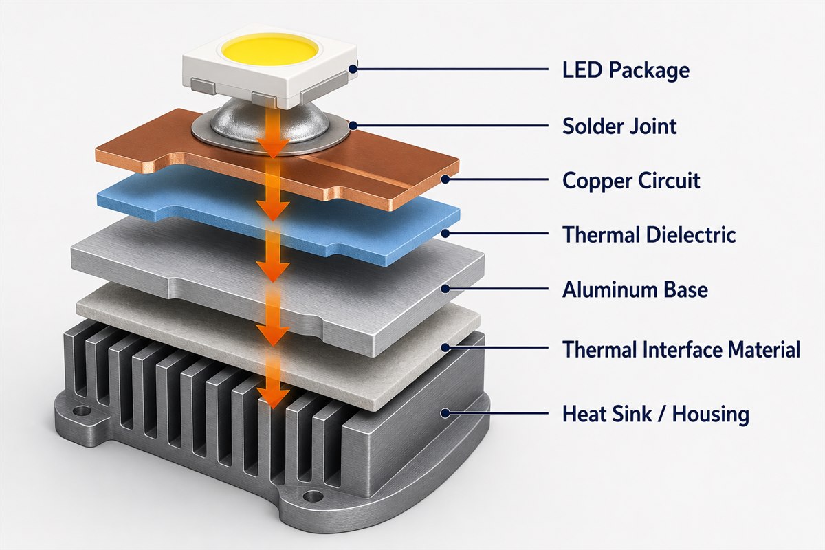
The basic heat path may look like this:

  • The component generates heat.
  • Heat moves through the solder joint.
  • Heat enters copper pads or copper planes.
  • Copper spreads the heat across a larger area.
  • Heat moves into the PCB base, heat sink, housing, or air.

This is why PCB thermal design often uses large copper pours, thicker copper, thermal vias, copper base materials, or metal core PCBs. Copper gives heat a faster path than FR4 alone.

However, copper must be placed correctly. A small copper trace may not carry enough heat away from a high-power part. A larger copper area, better via structure, or direct thermal contact may be required.

Is Copper a Good Conductor of Electricity and Heat?

Yes, copper is a good conductor of electricity and heat. This combination is one reason copper is so common in electrical and electronic products.

Copper is used for electrical conduction because it has low electrical resistivity. Less resistance means less power loss and less unwanted heat generation. Copper is also used for thermal conduction because it can spread heat efficiently.

In PCB and PCBA projects, these two properties often work together:

  • Copper traces carry current.
  • Copper planes distribute power and ground.
  • Copper pours spread heat.
  • Thermal vias move heat between layers.
  • Copper thickness affects current capacity and temperature rise.
  • Copper base PCBs improve heat dissipation in high-power applications.

For example, a power board may need both high current capacity and thermal control. In that case, the engineering team may review copper thickness, trace width, copper balance, via count, thermal relief, solder mask opening, and heat sink connection together.

This is why copper selection is not only a material choice. It is part of the electrical, thermal, and manufacturing design of the product.

Why Is Copper a Good Conductor of Heat and Electricity?

Copper conducts both heat and electricity well because of its electron structure. Copper atoms provide mobile electrons that can move through the metal with relatively low resistance. These mobile electrons carry electrical charge and also transfer thermal energy.

This explains why good electrical conductors are often good heat conductors. Silver, copper, gold, and aluminum all conduct both electricity and heat well, although their cost, strength, weight, corrosion behavior, and manufacturing use cases differ.

Copper is especially popular because it offers a strong balance of:

  • High electrical conductivity
  • High thermal conductivity
  • Good availability
  • Reasonable cost compared with silver
  • Good solderability
  • Good manufacturability
  • Wide use in PCB fabrication

In electronics, this balance matters. Silver may conduct better than copper, but it is too expensive for most PCB and power electronics structures. Aluminum is lighter and cheaper, but copper usually provides better conductivity and easier soldering in PCB applications.

For many PCB projects, copper remains the practical choice for current flow and heat spreading.

Is Copper a Very Good Conductor of Heat Compared With Other Metals?

Copper is a very good conductor of heat compared with most metals. Silver has higher thermal conductivity than copper, but copper is far more practical for most industrial and electronics applications. Aluminum also conducts heat well, but copper generally conducts heat better.

Approximate thermal conductivity values at room temperature are:

MaterialApprox. Thermal Conductivity
Silver~429 W/m·K
Copper~390-400 W/m·K
Aluminum~205-237 W/m·K
Brass~100-120 W/m·K
Iron~80 W/m·K
Stainless steel~15-25 W/m·K
FR4 laminateMuch lower than metals

These values can vary by alloy, purity, temperature, and material condition. Still, the ranking is clear: copper is among the best practical heat-conductive metals.

For PCB manufacturing, the comparison is important because different materials serve different roles. FR4 provides insulation and mechanical support, but it does not conduct heat well. Copper provides the electrical and thermal path. Aluminum or copper base materials may be used when a normal FR4 board cannot move heat away fast enough.

Is Copper a Good Conductor of Heat

Copper vs Aluminum and Iron for Heat Conduction

Copper conducts heat better than aluminum and iron in most common engineering comparisons. This is why copper is often used when fast heat spreading is needed.

Copper vs aluminum:

  • Copper has higher thermal conductivity.
  • Aluminum is lighter.
  • Aluminum is usually cheaper.
  • Copper is easier to solder in PCB manufacturing.
  • Aluminum is common in metal core PCB bases and heat sinks.
  • Copper is common in traces, planes, vias, and copper base PCBs.

Copper vs iron:

  • Copper conducts heat much better than iron.
  • Iron is stronger and more structural.
  • Iron is not commonly used as a PCB thermal conductor.
  • Copper is better for electrical and thermal conduction.

This does not mean copper is always the best choice for every part. Aluminum may be better for lightweight heat sinks. Stainless steel may be better for mechanical strength and corrosion resistance. Ceramic may be better for insulation and thermal stability in some high-power modules.

The right material depends on the product goal. In PCB thermal management, copper is usually used where electrical and thermal paths must be efficient.

Why Copper Heat Conductivity Matters in PCB Design

Copper heat conductivity matters in PCB design because many electronic components generate heat during operation. If heat is not moved away efficiently, component temperature rises, performance changes, and long-term reliability can drop.

Heat-sensitive PCB applications include:

  • High-power LED boards
  • Power supplies
  • Motor control boards
  • Battery management systems
  • Automotive electronics
  • Industrial controllers
  • RF power modules
  • Charging equipment
  • Ceramic PCB modules
  • Metal core PCBs

In these products, copper can help reduce hot spots and spread heat over a larger area. But copper alone is not enough. The PCB layout and stackup must provide a complete thermal path.

Important PCB thermal design choices include:

  • Copper thickness
  • Copper area
  • Trace width
  • Copper plane design
  • Thermal vias
  • Via filling or plugging
  • Solder mask opening
  • Component pad design
  • Metal core material
  • Heat sink or housing contact

At EBest Circuit, our engineering team reviews copper thickness, stackup, component power, thermal requirements, and manufacturability together. This helps customers avoid designs that look acceptable electrically but fail because of temperature rise.

How Copper Helps PCB Heat Dissipation in Real Products

Copper helps PCB heat dissipation by spreading heat from hot components into a larger conductive area. The larger the effective copper area and the better the thermal path, the easier it is to reduce localized hot spots.

For standard FR4 PCBs, copper can help through:

  • Wider traces
  • Large copper pours
  • Internal copper planes
  • Thermal vias under power components
  • Heavier copper layers
  • Better copper balance

For higher-power products, a standard FR4 PCB may not be enough. In those cases, engineers may consider:

  • Aluminum metal core PCB
  • Copper base PCB
  • Ceramic PCB
  • Thick copper PCB
  • Thermal interface material
  • Heat sink integration
  • One-stop PCB and PCBA thermal review

For example, a high-power LED module may need a metal core PCB to move heat from the LED pad into the metal base. A power module may need heavy copper traces and thermal vias. A ceramic PCB may be selected when the design needs insulation, high thermal conductivity, and thermal stability.

EBest Circuit provides FR4 PCB, metal core PCB, ceramic PCB, special PCB, PCB prototype, mass production, component sourcing, and PCB assembly services. For thermal projects, we can review whether the copper structure, material, and assembly process match the actual heat dissipation requirement.

Is Copper a Good Conductor of Heat

FAQs About Copper as a Heat Conductor

Is copper a good conductor of heat?

Yes. Copper is a very good conductor of heat, with thermal conductivity around 390 to 400 W/m·K at room temperature. It transfers heat much better than iron, stainless steel, FR4, plastic, and many other common materials.

Why is copper a good conductor of heat?

Copper is a good conductor of heat because it has mobile free electrons. These electrons move energy through the metal quickly, allowing heat to spread from hot areas to cooler areas.

Is copper a good conductor of electricity and heat?

Yes. Copper conducts both electricity and heat well. This is why it is widely used in wires, busbars, PCB traces, copper planes, heat spreaders, and power electronics.

Is copper better than aluminum for heat conduction?

Copper usually conducts heat better than aluminum, but aluminum is lighter and often cheaper. In PCB applications, copper is widely used for traces and planes, while aluminum is often used as the base material in aluminum metal core PCBs.

Why does copper heat conductivity matter in PCBs?

Copper heat conductivity matters because PCB components can generate heat during operation. Copper traces, planes, pours, thermal vias, and metal core structures help move heat away from components and improve reliability.

Can EBest Circuit help with copper-based PCB heat dissipation?

Yes. EBest Circuit can support PCB fabrication, copper thickness review, metal core PCB, ceramic PCB, component sourcing, SMT assembly, DFM review, and PCBA testing for products that need better heat dissipation.

If your PCB project depends on copper heat conductivity, thermal vias, heavy copper, metal core PCB, ceramic PCB, or PCBA heat dissipation, send your Gerber files, stackup, BOM, drawings, and thermal requirements to sales@bestpcbs.com. Our team will help you review a practical path from prototype to production.

You may also like

Custom PCB Design for Sensors: Signal, Power and Test Checks

July 13th, 2026
Custom sensor PCB design workbench with sensor board, oscilloscope and enclosure parts

Custom PCB design for sensors should be reviewed around signal accuracy, low-noise power, grounding, connector placement, calibration access, test points, environmental protection and production-ready RFQ files. A sensor PCB is not only a small carrier board for a sensing element. It is the interface between the real world and the electronics that must read that signal consistently.

This guide is written for engineers and buyers preparing a custom sensor PCB or sensor PCBA for industrial devices, IoT products, environmental monitoring, equipment controls, medical-adjacent instruments, automotive modules or field equipment. It focuses on manufacturable board design and supplier review, not on selecting one specific sensor IC.

What does custom PCB design for sensors need to solve?

A sensor PCB needs to preserve the signal the sensor produces while surviving the mechanical, electrical and environmental conditions around the final product. The board may measure temperature, pressure, humidity, light, motion, gas, current, position or vibration, but the design checks follow a similar pattern: protect the signal path, control noise, provide stable power and make the board testable.

Low-current analog sensors may need guarded routing, short high-impedance traces and careful leakage control. Digital sensors may need clean I2C, SPI, UART, CAN, RS-485 or wireless module routing. Compact sensor products may use an HDI PCB when the enclosure is tight and the connector, MCU, RF section and sensing element compete for space.

Sensor board area PCB design check Buyer or engineer risk
Signal path Short routing, shielding, filtering, impedance or guard traces when needed Noise, drift or unstable readings can hide the real sensor output
Power supply Low-ripple rails, local decoupling, regulator heat and startup behavior Power noise can show up as false measurement changes
Grounding Analog/digital return paths, chassis connection and cable shield plan Ground loops or poor return paths can create hard-to-debug faults
Environment Coating, enclosure interface, sensor exposure window and connector sealing Humidity, dust, chemicals or vibration can change readings or damage the board
Production test Test pads, calibration points, programming access and fixture clearance Good prototypes can become slow or inconsistent in volume builds

Which sensor applications need a custom PCB?

A custom PCB is useful when the sensor board must fit a product enclosure, meet a specific noise target, connect to a harness, support calibration or survive a defined operating environment. Evaluation boards are useful for early testing, but they rarely match the size, connector, grounding, power and protection requirements of the final product.

Common examples include environmental sensor nodes, industrial monitoring modules, battery and charger sensors, flow meters, load-cell interfaces, motor feedback boards, optical sensor boards, wearable sensor modules and equipment health monitoring electronics. Many designs can use an FR4 Printed Circuit Board. High-frequency, wireless or antenna-connected sensor products may need RF material decisions, controlled routing or a review against an RF PCB capability page.

How should low-noise layout be planned?

Low-noise sensor layout starts with floorplanning: keep the sensor front end, reference, ADC, filter, connector and noisy switching circuits in controlled zones. A layout can pass a simple connectivity check but still produce unstable data if switching regulators, antennas, motors, relays or long cable inputs couple noise into the measurement path.

Custom sensor PCB DFM review with schematic, connector cables and layout notes
Sensor PCB design should be reviewed as a complete signal chain, not only as a component placement task.

Place the sensor and analog front end close together when the signal is small. Keep high-current switching loops away from sensitive inputs. Use a continuous reference plane where possible, and avoid splitting a return path under critical traces without a clear reason. For cable-connected sensors, review ESD, surge, filtering and shield termination before release. If the design uses a flex tail or adhesive-mounted sensing element, confirm bend area, stiffener position and assembly handling early.

What power and grounding checks matter most?

Power and grounding checks should answer whether the sensor reading stays stable during startup, load changes, communication bursts and nearby switching events. Sensors that look accurate on a bench supply can become noisy when they share power with radios, relays, motors, LEDs, heaters or long cable harnesses.

Ask the designer or supplier to review regulator choice, decoupling placement, reference voltage routing, ground return, cable shield strategy and any required isolation. If a sensor board includes both sensitive analog inputs and digital communication, the layout should support both signal integrity and production assembly. When the order includes SMT, through-hole parts, connectors and final inspection, discuss the project as a Prototype PCB Assembly or production PCBA job instead of a bare PCB only.

How should connectors, cables and enclosures be designed?

Sensor PCB reliability often depends on connector orientation, cable strain relief, enclosure clearance and how the sensor is exposed to the measured environment. A board can be electrically correct but hard to assemble if the cable exits the wrong side, the sensor window does not align, or the test pads are blocked by the housing.

Before fabrication, compare the PCB outline with the enclosure model, mounting bosses, gasket, sensor opening, cable routing and service access. For field devices, define whether the board needs conformal coating, potting, a vented enclosure, connector sealing or a separate daughterboard. If the supplier is expected to assemble the PCB into a housing or harness, treat the RFQ as a Box Build Assembly discussion.

When do flex or rigid-flex sensor boards make sense?

Flex and rigid-flex sensor boards make sense when the sensing element must sit away from the main electronics, bend around a shape, reduce connector count or fit a compact enclosure. They are common in wearables, medical-adjacent devices, compact industrial sensors, optical modules, probes and adhesive-mounted sensing assemblies.

Flex is not a shortcut around mechanical design. Bend radius, copper direction, stiffener location, adhesive choice, strain relief and assembly sequence still need review. If a sensor product uses a flexible circuit, compare the design against a proven custom flex PCB design checklist before ordering production tooling.

What should be included in the sensor PCB test plan?

The test plan should prove that the board can be fabricated, assembled, programmed, calibrated and checked repeatedly before it reaches the final product. For sensor PCBA, continuity alone is usually not enough. The test may need known input conditions, reference measurements, firmware loading, communication checks and pass/fail limits.

Sensor PCBA functional testing with oscilloscope, test fixture and environmental sensor enclosure
Plan functional test and calibration access before the board is released for production.

Add test pads for power rails, ground, programming, communication lines and critical analog nodes. Keep them reachable after assembly and enclosure installation. If calibration is needed, define the calibration input, equipment, firmware state and acceptable tolerance. A supplier’s PCB test equipment and fixture planning should be discussed before volume production, not after failed boards appear.

RFQ checklist for custom sensor PCB design

A strong RFQ package lets the supplier review sensor accuracy, manufacturability, assembly risk and test coverage before quoting price and lead time. Send controlled files instead of screenshots or partial exports.

  1. Gerber files, drill files, netlist and controlled revision number.
  2. Schematic, stackup, copper weight, board thickness and surface finish requirement.
  3. Sensor type, expected signal range, accuracy goal and calibration requirement.
  4. Power input range, current load, regulator notes and any battery or charger interface.
  5. Connector, cable, enclosure, coating, potting or gasket information.
  6. BOM, approved alternates, centroid file and assembly drawing for PCBA.
  7. Programming method, firmware loading requirement and functional test criteria.
  8. Environmental notes such as temperature, humidity, vibration, dust, chemicals or outdoor exposure.

Supplier questions buyers should ask

The best supplier questions force a real DFM and test review instead of a generic board price. Use them before approving the first build.

  • Which parts of this sensor design create the highest layout or assembly risk?
  • Are the sensor, connector and enclosure clearances consistent with the mechanical file?
  • Do any analog inputs need additional spacing, guarding, shielding or cleaning controls?
  • Are the test pads reachable after assembly and enclosure installation?
  • Which components have sourcing risk or need approved alternates?
  • Can the test fixture simulate or verify the sensor input reliably?
  • What should change before moving from prototype to pilot production?

Sensor boards often depend on stable parts. If a project uses specialized sensor ICs, connectors, filters, references or wireless modules, involve Component Sourcing early so substitutes do not change measurement behavior without engineering approval.

FAQ

What is custom PCB design for sensors?

Custom PCB design for sensors means designing a circuit board around a sensing element, signal chain, power system, connectors, firmware access and test plan for a specific product. The goal is to read the sensor accurately and build the board repeatedly, not just connect a sensor IC to a controller.

Does every sensor PCB need a four-layer board?

No. Simple low-speed digital sensor boards may work on two layers when routing, power and grounding are clean. Mixed-signal, wireless, compact or low-noise sensor boards often benefit from four or more layers because a stable reference plane and controlled return paths reduce layout risk.

What causes noise in sensor PCB readings?

Common causes include unstable power rails, poor grounding, long high-impedance traces, switching regulator noise, nearby motors or relays, cable pickup, weak shielding, poor filtering and bad test setup. The fix depends on the sensor type and signal level, so schematic and layout review should happen before fabrication.

What files are needed for a sensor PCB quote?

Send Gerber and drill files, schematic, stackup, board drawing, BOM, centroid file, assembly drawing, enclosure notes and test requirements. If calibration, coating, potting, firmware loading or box build is required, include those details in the first RFQ.

Can a PCB supplier improve sensor accuracy?

A PCB supplier can help with manufacturability, material choice, assembly quality, inspection and repeatable testing. Accuracy still depends on the sensor IC, circuit design, layout, calibration method, firmware and operating environment. Treat supplier feedback as one part of the engineering review.

Conclusion

Custom PCB design for sensors should start with the measurement problem, not with board price. Define the signal, power rails, grounding, enclosure, connector, calibration and test plan before production files are released. Then ask the supplier to review manufacturability and assembly risk against the real use case. That process gives the sensor board a better chance of producing stable readings in the final product.

You may also like

Custom PCB Design for Mining: Dust, Vibration and Power Checks

July 13th, 2026
Custom PCB design for mining equipment with rugged enclosure and connector harness

Custom PCB design for mining equipment should be reviewed around dust, moisture, vibration, protected power input, connector strain relief, thermal control, test points and production-ready RFQ files. A mining electronics board is not only a circuit layout. It is part of a rugged system that may sit near motors, pumps, sensors, conveyors, vehicles, lighting, chargers or communication devices where contamination, shock and repair access matter.

This guide is written for engineers and buyers preparing a custom PCB or PCBA for mining-related equipment. It focuses on practical design and manufacturing checks before fabrication or assembly. If the product will be used underground, near combustible dust, or in another regulated hazardous area, confirm the applicable equipment-level certification requirements with your compliance team. A PCB supplier can support design for reliability, traceability and production quality, but board fabrication alone does not certify the complete mining device.

What does custom PCB design for mining need to solve?

Mining PCB design needs to keep electrical performance stable while the board is exposed to dust, vibration, heat, moisture, long cable runs and maintenance stress. The exact risks depend on whether the board is used in a sensor node, motor controller, lighting module, communication gateway, battery system, display panel or test device.

For a simple monitoring module, the main issues may be enclosure fit, connector sealing and low-power reliability. For a power or drive-related board, the review moves toward copper weight, creepage and clearance, thermal paths and protection components. Compact control electronics may also need an HDI PCB if the enclosure is tight and the component density is high.

Mining design risk PCB or PCBA check Why it matters
Dust and moisture Enclosure interface, coating decision, connector sealing and cleaning process Contamination can create leakage paths, corrosion and intermittent faults
Vibration and shock Mounting holes, board support, connector retention and heavy component placement Loose connectors or cracked solder joints can stop equipment in the field
Power variation Input protection, grounding, copper width, fusing and transient protection Long cables and inductive loads can create voltage stress
Heat buildup Copper weight, thermal vias, enclosure contact and material selection Sealed boxes often have limited airflow
Maintenance Test points, labels in drawings, harness plan and replaceable modules Field teams need faults isolated quickly without damaging the board

Where are custom mining PCBs used?

Custom mining PCBs are common in control, sensing, communication, lighting, power conversion and equipment monitoring devices. A buyer should define the use case before asking for a quote, because a sensor interface board and a high-current control board need different materials, copper rules and test plans.

Typical examples include conveyor monitoring electronics, pump controllers, battery management devices, rugged displays, LED lighting modules, wireless gateways, environmental sensors and vehicle-mounted control units. Some designs use standard FR4 PCB construction. Others need heavier copper, higher Tg material, metal-backed structures, conformal coating, sealed box integration or full PCBA support.

How should dust, moisture and enclosure fit be handled?

The PCB should be designed together with the enclosure, gasket, connector system and cleaning/coating plan. Treating the board as a flat electrical drawing and the enclosure as a later mechanical decision often creates failures at cable entries, mounting bosses, edge clearance and service access.

Engineers reviewing a rugged mining equipment PCB with enclosure gasket and connector samples
Mining electronics should be reviewed as a board, enclosure, connector and testable assembly, not as a bare PCB only.

Before layout release, check the board outline against the enclosure drawing, connector keepout area, mounting-hole tolerance, coating keepout, service connector position and any pressure-equalization or sealing requirement. If conformal coating is planned, mark no-coat areas around connectors, switches, programming pads and test contacts. If potting is planned, confirm component height, thermal behavior and repair expectations before the production file is frozen.

What vibration checks matter before production?

Vibration risk is controlled by board support, connector retention, solder joint protection and heavy component placement. A mining PCB can pass an electrical review and still fail in the field if a large inductor, terminal block, relay, transformer, battery connector or harness load is not mechanically supported.

Use larger mounting margins around high-stress areas. Keep heavy parts away from unsupported board edges when possible. Add strain relief for harnesses instead of letting cable pull act directly on solder joints. For mixed SMT and through-hole designs, define whether wave soldering, selective soldering or hand operations are expected. If the design includes high-current terminals, compare the copper and spacing assumptions against a relevant design reference such as the Heavy Copper PCB Design Guide.

How should power input and heat be reviewed?

Power input review should cover voltage range, surge exposure, reverse polarity risk, grounding, heat flow and copper current capacity. Mining equipment often connects through long cables, battery systems, motors, relays, lighting modules or chargers. These conditions can put more stress on input circuits than a clean lab supply.

For early DFM, send the supplier the expected operating voltage, maximum current, copper weight, target temperature range, board thickness, surface finish and any thermal interface to the enclosure. Do not ask for only a bare board price if the real product needs heat-spreading, coated assembly, heavy connectors or functional testing. The quote should reflect the way the board will be used.

Design area Questions to answer before RFQ
Input power What voltage range, current load, fuse strategy and reverse-polarity protection are required?
Grounding How are chassis ground, signal ground and shield termination handled?
Thermal path Will heat leave through copper pours, vias, thermal pads, an enclosure wall or a heatsink?
Copper weight Are high-current traces sized for the real load and temperature rise target?
Protection Are surge, ESD and inductive switching risks reviewed at cable and connector interfaces?

Which materials and stackups fit mining electronics?

The material choice should follow the electrical load, enclosure temperature, vibration risk and required board density. FR4 is often suitable for control and sensor boards, but high-current, high-heat or compact assemblies may need different copper, laminate, via and thermal decisions.

For dense signal boards, HDI can reduce routing congestion and help fit a smaller rugged enclosure. For power boards, thicker copper, larger spacing and thermal planning may matter more than density. For LED lighting or heat-generating modules, metal-backed or direct thermal path designs may be considered. The right choice depends on the project files, not on a generic mining label.

How should assembly and sourcing be planned?

Mining PCBA planning should include component availability, substitute approval, coating or sealing steps, test fixture needs and final box-level handling. A bare PCB schedule does not describe the finished product if the order also needs SMT, through-hole assembly, wiring, enclosure fit or functional testing.

Before releasing the order, provide a controlled BOM, approved alternates, centroid file, assembly drawing, polarity notes, connector orientation, firmware loading requirement and test criteria. If long-life parts or industrial-grade components are required, discuss Component Sourcing early. If the supplier is expected to deliver a mounted board in a sealed housing, treat it as a Box Build Assembly discussion rather than a normal PCB-only purchase.

What test plan should be ready before release?

The test plan should prove the board can be built, inspected and checked consistently before it reaches the field. At minimum, define electrical test for bare boards, AOI or visual inspection for assembly, functional checks for powered boards and any project-specific connector, LED, sensor, relay or communication test.

Mining equipment PCB assembly under electrical test with rugged connector harness and sealed enclosure
Testing should be planned before production release, especially when cables, connectors, sealed boxes and field power inputs are involved.

Useful test points should be accessible after assembly, not hidden under large components or blocked by the enclosure. If the board has firmware, define how programming and verification are handled. If the product uses sensors, motors, relays or communication interfaces, list the pass/fail behavior in simple language. A supplier’s PCB test equipment capability should be part of the RFQ discussion when the board needs repeatable inspection instead of only continuity checks.

RFQ checklist for custom PCB design for mining

A useful RFQ package lets the supplier review reliability risks before quoting cost and lead time. Send the same controlled package to every supplier if you want to compare quotes fairly.

  1. Gerber files, drill files, netlist and controlled revision number.
  2. Board drawing with thickness, outline tolerance, mounting holes and connector keepouts.
  3. Stackup, copper weight, material preference and surface finish requirement.
  4. Expected operating voltage, current load, thermal concern and enclosure notes.
  5. BOM, approved substitutes, centroid file and assembly drawing if PCBA is included.
  6. Coating, potting, cleaning, labeling, packaging or box-build requirements.
  7. Test plan with required measurements, programming steps and pass/fail criteria.
  8. Compliance notes for the final equipment, especially if the use environment is regulated.

Supplier questions buyers should ask

The best supplier questions are specific enough to reveal whether the factory has reviewed the board as a mining electronics assembly, not just a generic PCB. Use the questions below before approving production.

  • Which part of this design creates the highest manufacturing risk?
  • Are the mounting holes, edge clearances and connector keepouts suitable for the enclosure?
  • Is the copper weight enough for the stated current and temperature target?
  • Do any components need adhesive, mechanical support or layout changes for vibration?
  • Which components have sourcing risk, and are substitutes already approved?
  • Can the test points still be reached after assembly or box build?
  • What should be changed before moving from prototype to production?

FAQ

What is custom PCB design for mining?

Custom PCB design for mining means designing a circuit board or PCBA for equipment used around mining operations, such as sensors, controllers, lighting, communication modules, power electronics or monitoring devices. The design must consider dust, vibration, moisture, power stress, enclosure fit, connectors, testing and production repeatability.

Does a mining PCB need a special material?

Not always. Many mining control or sensor boards can use FR4 when the electrical load and temperature are moderate. High-current, high-heat, compact or harsh-environment designs may need heavier copper, higher-grade laminate, HDI, metal-backed construction, coating or a different stackup. The material should follow the real design risk.

Can a PCB supplier certify mining equipment?

A PCB supplier can support reliable board fabrication, assembly, traceability, inspection and documentation. Certification for equipment used in regulated mining or hazardous environments is usually a system-level issue. Confirm ATEX, IECEx, MSHA or local requirements with qualified compliance specialists before production decisions.
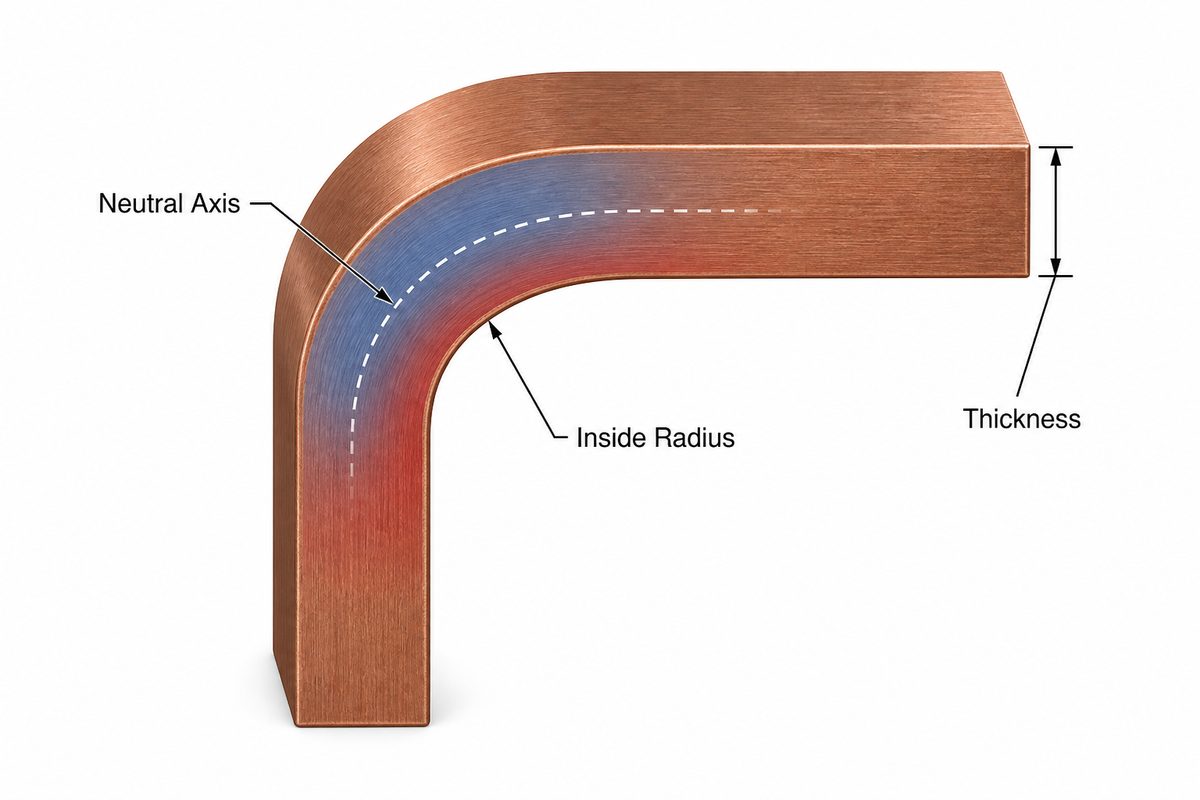
What files are needed for a mining PCB quote?

Send Gerber files, drill files, board drawing, stackup, copper weight, surface finish, BOM, centroid file, assembly drawing, enclosure notes and test requirements. If the board will be coated, potted or installed in a sealed box, include those details in the first RFQ instead of adding them later.

What causes delays in mining PCB projects?

Common delays include unclear enclosure drawings, missing connector orientation, unapproved component substitutes, vague test criteria, incomplete power requirements and late coating or box-build decisions. A controlled RFQ package helps the supplier check manufacturability before committing to lead time.

Conclusion

Custom PCB design for mining should be treated as a rugged electronics project, not a normal board order with a different label. Start with the environment, enclosure, connectors, power input, heat path, component sourcing and test plan. Then ask the supplier to review the files for manufacturability before quote approval. That process gives the buyer a better chance of receiving a board that can be assembled, inspected and supported in real mining equipment.

You may also like

Why Is Astra MT77 Suitable for RF and mmWave PCB Designs?

July 13th, 2026

Astra MT77 is an ultra-low-loss laminate and prepreg system for RF, microwave and mmWave PCB designs. Its low Df and stable Dk help control signal loss, impedance and phase at high frequencies.

Unlike standard FR-4, this material targets circuits where dielectric behavior directly affects signal quality. Core thickness, prepreg construction, copper roughness and process control still determine final PCB performance.

This guide explains material properties, Dk and Df, stackup selection, controlled impedance and common applications. It also covers cost, material comparison and PCB sourcing.

Astra MT77, https://www.bestpcbs.com/blog/2026/07/astra-mt77/

What Is Astra MT77 PCB Material?

Astra MT77 is an ultra-low-loss RF and microwave laminate and prepreg material for high-frequency PCB applications. It is selected when stable impedance and low dielectric loss matter more than standard FR-4 cost.

The material is positioned as an alternative to PTFE and other commercial microwave laminates. Its fabrication is compatible with standard FR-4 PCB processing methods.

Typical values include Dk 3.00, Df 0.0017, Tg 200°C and Td 360°C. These properties support demanding RF and mmWave PCB structures.

In practice, the material often sits on critical RF or antenna layers. A hybrid stackup can use compatible materials on digital or control layers to reduce total material cost.

Why Is Astra MT77 Suitable for RF and mmWave PCB Designs?

Astra MT77 combines ultra-low dielectric loss, stable Dk and practical multilayer processing. This balance matters at high frequencies, where small material changes can affect loss and phase.

The main advantages include:

  • Low dielectric loss: A typical Df of 0.0017 helps reduce dielectric loss.
  • Stable Dk: A typical Dk of 3.00 supports predictable impedance and electrical length.
  • W-band capability: The material supports demanding RF, microwave and mmWave structures.
  • Temperature stability: Dk remains stable from -40°C to +140°C up to W-band frequencies.
  • Smooth copper support: HVLP copper can reduce conductor-loss effects at high frequencies.
  • Multilayer flexibility: Laminate and prepreg forms support complex RF PCB stackups.
  • FR-4 process compatibility: Fabrication is less specialized than many PTFE material systems.

The main advantage is the balance of low loss, electrical stability and practical PCB processing.

Isola Astra MT77 Datasheet Overview: What Are the Main Material Properties?

The Isola Astra MT77 datasheet combines electrical, thermal and reliability data needed for high-frequency PCB material review. The table below summarizes the main published typical values.

PropertyTypical ValueTest Method
Tg by DSC200°CIPC-TM-650 2.4.25C
Td at 5% Weight Loss360°CIPC-TM-650 2.4.24.6
T260>60 minIPC-TM-650 2.4.24.1
T288>60 minIPC-TM-650 2.4.24.1
Z-Axis CTE Pre-Tg50–70 ppm/°CIPC-TM-650 2.4.24C
Z-Axis CTE Post-Tg250–350 ppm/°CIPC-TM-650 2.4.24C
X/Y-Axis CTE Pre-Tg12 ppm/°CIPC-TM-650 2.4.24C
Thermal Conductivity0.45 W/m·KASTM E1952
Thermal StressPass, 10 s at 288°CIPC-TM-650 2.4.13.1
Dk3.00IPC-TM-650 2.5.5.5
Df0.0017Bereskin Stripline
Volume Resistivity1.33 × 10⁷ MΩ·cmIPC-TM-650 2.5.17.1
Surface Resistivity1.33 × 10⁵ MΩIPC-TM-650 2.5.17.1
Dielectric Breakdown45.4 kVIPC-TM-650 2.5.6B
Electric Strength45 kV/mmIPC-TM-650 2.5.6.2A
Peel Strength1.0 N/mmIPC-TM-650 2.4.8.3
Moisture Absorption0.1%IPC-TM-650 2.6.2.1A
FlammabilityV-0UL 94
RTI130°CUL 796

Dk and Df define the core RF behavior. Tg, Td, CTE and thermal stress help assess multilayer and assembly reliability.

Astra MT77 Material Properties, https://www.bestpcbs.com/blog/2026/07/astra-mt77/

What Are the Dielectric Constant and Dissipation Factor of Astra MT77?

The typical Astra MT77 dielectric constant is 3.00, while the typical dissipation factor is 0.0017. These values affect impedance, electrical wavelength and dielectric loss.

Dk affects impedance and electrical length. Use the selected material value in microstrip, stripline and grounded coplanar waveguide calculations.

Df represents dielectric signal loss. The low dissipation factor helps limit loss as frequency and trace length increase.

However, do not assume every dielectric layer has exactly the same Dk. Published prepreg constructions range from Dk 2.91 to 3.01.

For controlled impedance, use the selected construction and final pressed dielectric thickness. This gives a more realistic model than one generic material value.

How to Choose the Right Astra MT77 Thickness for a PCB Stackup?

Choose Astra MT77 thickness from impedance, RF geometry, operating frequency and final PCB construction. The thinnest core is not automatically the best option.

  • Start with the target impedance: Define 50 Ω, 75 Ω or the required differential impedance first.
  • Review published core thicknesses: Standard core data includes 0.064 to 1.524 mm constructions.
  • Check practical trace width: Very thin dielectrics may force narrow traces with tighter etching tolerance.
  • Match the RF structure: Microstrip, stripline and grounded coplanar waveguide need different dielectric spacing.
  • Model prepreg separately: Published prepreg constructions use Dk values from 2.91 to 3.01.
  • Use realistic pressed thickness: Resin content, copper pattern and lamination affect finished dielectric spacing.
  • Check total PCB balance: Keep copper distribution and dielectric construction mechanically balanced.
  • Freeze the approved stackup: Late core or prepreg changes can alter impedance and electrical length.

The right thickness produces a manufacturable RF geometry with stable dielectric spacing.

Astra MT77 Thickness for PCB Stackup, https://www.bestpcbs.com/blog/2026/07/astra-mt77/

How Should an Astra MT77 PCB Be Designed for Controlled Impedance?

An Astra MT77 PCB should use a fixed stackup, exact dielectric construction and realistic finished copper geometry. Generic material values can create avoidable impedance error.

  • Use construction-specific Dk: Match the model to the selected core or prepreg construction.
  • Enter finished dielectric thickness: Use the expected pressed thickness, not only nominal raw material data.
  • Include finished copper thickness: Base copper and plating change the final trace cross-section.
  • Control copper roughness: HVLP copper is relevant when conductor loss becomes significant.
  • Keep reference planes continuous: Avoid plane splits below critical RF traces and launches.
  • Limit unnecessary layer changes: RF vias add inductance, capacitance and return-path discontinuities.
  • Model connectors and launches: Include pads, antipads, transitions and nearby ground vias.
  • Review solder mask coverage: Coating can change the local dielectric environment around surface RF lines.
  • Add representative coupons: Match coupon layers, copper thickness and dielectric construction to the PCB.
  • Set realistic fabrication tolerances: Line width and dielectric variation must fit the design margin.

At mmWave frequencies, the complete transmission structure affects impedance. Material data, geometry and fabrication control must work together.

How Do Tg, Td and Thermal Conductivity Affect Astra MT77 PCB Reliability?

Astra MT77 has a typical Tg of 200°C, Td of 360°C and thermal conductivity of 0.45 W/m·K. These values describe different reliability limits.

  • Tg 200°C: A high Tg helps limit major expansion changes during thermal processing.
  • Td 360°C: Td indicates material decomposition behavior at 5% weight loss.
  • T260 and T288 above 60 minutes: These values indicate resistance to delamination under the stated TMA method.
  • Thermal stress pass at 288°C for 10 seconds: This supports lead-free process evaluation.
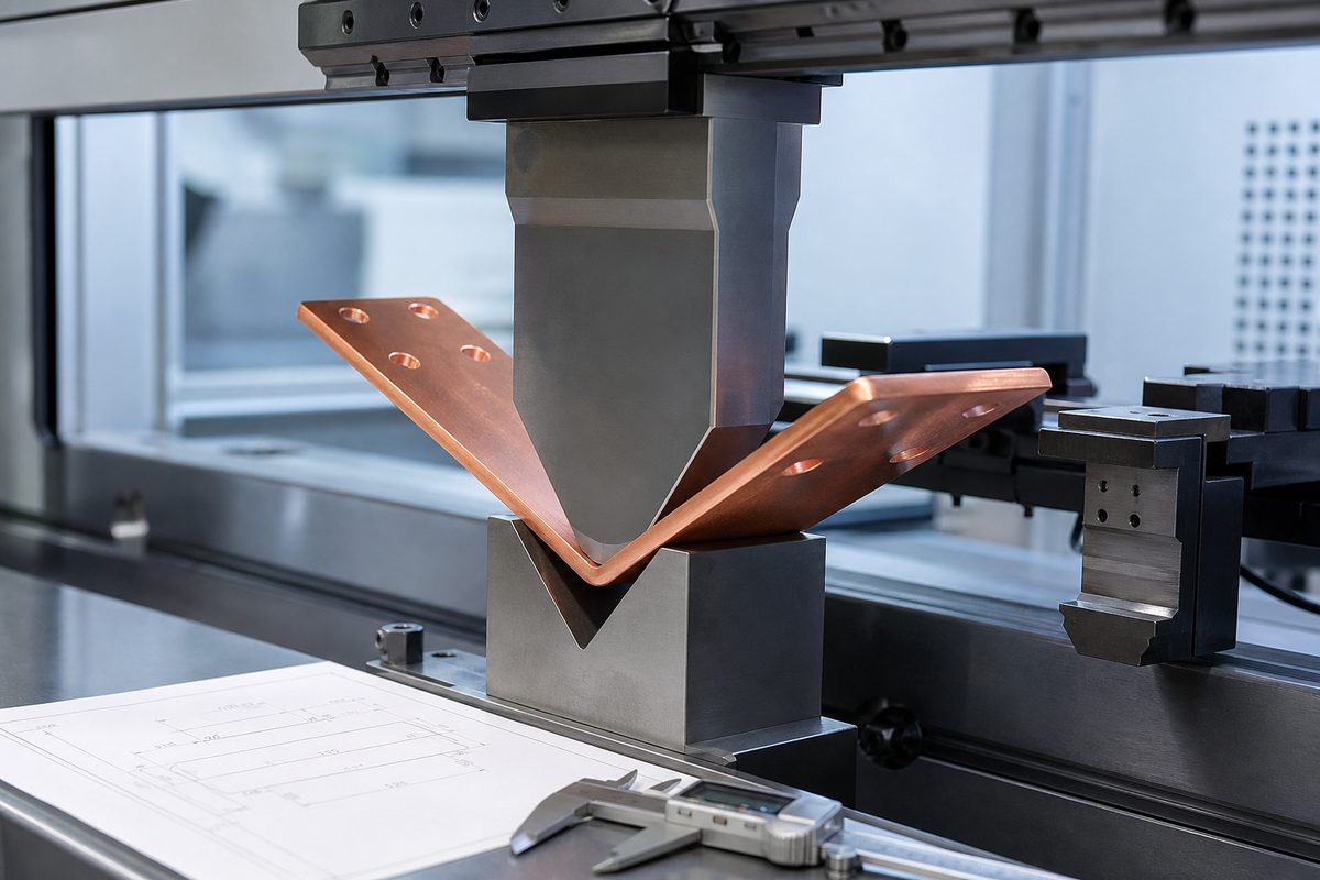
  • Z-axis CTE of 50–70 ppm/°C pre-Tg: Lower expansion before Tg helps plated-hole reliability.
  • Post-Tg Z-axis CTE of 250–350 ppm/°C: Expansion rises after Tg and still matters during heat exposure.
  • Thermal conductivity of 0.45 W/m·K: The dielectric conducts heat but is not a dedicated heat spreader.
  • Moisture absorption of 0.1%: Low moisture uptake helps support stable material behavior.

Tg and Td are not the continuous operating temperature of a finished PCB. System thermal limits must be based on the complete assembly.

What Applications Commonly Use Astra MT77 PCB Material?

Common applications include:

  • 77 GHz automotive radar
  • Adaptive cruise control systems
  • Pre-crash radar electronics
  • Blind-spot detection systems
  • Lane departure warning electronics
  • Stop-and-go radar systems
  • Long RF antenna structures
  • Commercial RF and microwave circuits
  • Aerospace and defense RF electronics

The material is most useful where low RF loss and stable high-frequency behavior create measurable system value.

Astra MT77 vs I-Tera MT40: Which Material Should You Choose?

Choose Astra MT77 when ultra-low RF and mmWave loss is the main priority. Choose standard I-Tera MT40 for broader high-speed digital and RF PCB designs.

The comparison below uses standard I-Tera MT40 laminate and prepreg data. The separate I-Tera MT40 RF/MW range includes additional Dk constructions.

PropertyAstra MT77I-Tera MT40
Primary FocusRF/MW and mmWaveHigh-speed digital and RF/MW
Dk3.003.45
Df0.00170.0031
Tg by DSC200°C215°C
Td360°C360°C
Thermal Conductivity0.45 W/m·K0.61 W/m·K
Dk Temperature Range-40°C to +140°C-55°C to +125°C
Frequency RangeUp to W-bandUp to W-band
Material FormsLaminate and prepregLaminate and prepreg
ProcessingFR-4 process compatibleNo special PTFE-type through-hole treatment
Best FitLoss-sensitive RF/mmWaveHSD, hybrid and RF/MW

MT77 has the lower published Df and suits loss-sensitive RF paths. This includes radar and mmWave transmission structures.

I-Tera MT40 offers a broader fit for high-speed digital and mixed RF designs. It also has a higher published thermal conductivity.

Do not substitute either material without recalculating the stackup. Their Dk values differ, so identical trace geometry will not produce the same impedance.

Astra MT77 vs I-Tera MT40, https://www.bestpcbs.com/blog/2026/07/astra-mt77/

What Affects Astra MT77 PCB and Laminate Cost?

Astra MT77 PCB cost depends on material construction, manufacturing complexity and RF control requirements. One price per square foot cannot represent every finished PCB project.

The main cost factors are:

  • Material construction and availability: Non-standard cores or prepregs may increase sourcing time.
  • Layer count: More layers increase material, lamination and inspection requirements.
  • Copper type: Smooth or low-profile copper can affect material cost and availability.
  • Controlled impedance tolerance: Tight limits require stackup review and coupon verification.

  • Fine RF geometry: Narrow traces and small gaps increase process control requirements.
  • Hybrid stackup complexity: Mixed materials require detailed lamination planning.
  • Order quantity: Prototype and batch orders use material differently.
  • Testing requirements: Microsection and impedance testing add inspection steps.

For an accurate laminate price, provide the exact material construction and order quantity. Finished PCB quotations also require Gerber data, stackup, copper weight and impedance targets.

Searches for MT77 price per square foot often overlook fabrication cost. Material price is only one part of the finished RF PCB cost.

Why Choose EBest Circuit as Your Astra MT77 PCB Manufacturer?

EBest Circuit helps reduce material, stackup and production risks before the PCB reaches volume manufacturing. Our China-based source factory supports custom production and global supply.

  • Reduce stackup errors before fabrication: We review dielectric thickness, copper weight and RF layer arrangement early.
  • Protect approved RF performance: Material traceability helps prevent uncontrolled laminate or prepreg substitution.
  • Improve impedance consistency: Stackup, trace geometry and coupon requirements are checked before production.

  • Move from prototype to batch production faster: One manufacturing route supports sample verification and volume transfer.
  • Simplify complex RF sourcing: Multilayer, hybrid and controlled-impedance PCB requirements can be reviewed together.
  • Match quality controls to the application: Electrical testing, microsection and impedance verification can follow project requirements.
  • Support regulated industry programs: Our quality systems include ISO 9001, IATF 16949, ISO 13485 and AS9100D.
  • Source directly from a China factory: Global supply is supported without false overseas factory or warehouse claims.

The benefit is lower production risk and better stackup control from quotation through batch manufacturing.

Send the approved material requirement, stackup and Gerber files for review. We can check manufacturability before production pricing is finalized.

FAQs About Astra MT77 PCB Material

Q1: Is Astra MT77 RoHS compliant?

A1: Yes. Astra MT77 is identified as RoHS compliant and is compatible with lead-free assembly. Finished PCB or PCBA compliance still depends on the full material set, surface finish, solder and components.

Q2: Which IPC specification recognizes MT77?

A2: The official material information lists IPC-4103/17. The applicable finished PCB acceptance or performance standard still depends on the product, industry and fabrication specification.

Q3: What UL recognition is listed for MT77?

A3: Isola lists UL File E41625 for the material. The published typical values table also lists a UL 94 V-0 flammability rating and 130°C RTI.

Q4: Is MT77 compatible with lead-free assembly?

A4: Yes. Lead-free assembly compatibility is listed as a product attribute. The datasheet also reports a 10-second thermal stress pass at 288°C under the stated test method.

Q5: What copper foil and copper weights are available?

A5: The datasheet lists HVLP copper at 2.5 µm Rz JIS or below as standard for 1 oz and below. Published copper weights range from 0.5 to 2 oz, with thinner foil also available.

Q6: Does MT77 always require plasma desmear?

A6: No. The material shows good response to chemical desmear. Plasma can improve thick or high-aspect-ratio holes. FR-4-level plasma etching is strongly recommended for laser microvias.

Q7: Can MT77 support HDI, any-layer and VIPPO structures?

A7: Yes. The datasheet lists HDI, any-layer and VIPPO compatibility. However, laser microvia cleaning, repeated lamination and plating still require process validation for the actual PCB construction.

Q8: Can MT77 be used through multiple lamination cycles?

A8: Yes. Multiple lamination cycles are listed among the material’s processing advantages. The lamination cycle still needs adjustment for package thickness and the selected multilayer construction.

Q9: How should MT77 prepreg be stored?

A9: Store prepreg at 23°C or below and below 50% humidity. Keep it in the original packaging until use. FIFO inventory control is also recommended.

Q10: Should opened MT77 prepreg be vacuum sealed?

A10: No. Remaining prepreg should be resealed in the original packaging with fresh desiccant. Isola’s processing guide specifically states not to vacuum seal MT77 prepreg.

Q11: How quickly should finished boards be processed after opening an MBB?

A11: The processing guide recommends processing within 168 hours when shop-floor conditions remain below 30°C and 60% RH. Opened MBBs should be resealed immediately after inspection.

Q12: What packaging is recommended for long shelf life?

A12: For high-temperature assembly and long shelf life, dry boards should use a Moisture Barrier Bag, Humidity Indicator Card and adequate desiccant. This helps limit moisture uptake during storage and shipment.

Q13: Is MT77 density published in the main datasheet?

A13: No. A typical MT77 density value is not listed in the main published property table. Do not copy a density value from another RF laminate for weight calculations.

Q14: What files should be sent for an MT77 PCB quotation?

A14: Send Gerber or ODB++ data, drill files, stackup, copper weight, finished thickness, quantity and impedance requirements. Also identify critical RF layers and the required material construction.

Q15: Can finished MT77 laminate use standard aqueous imaging and common etchants?

A15: Yes. Isola’s processing guide states that the laminate can use standard aqueous dry films. It is also compatible with cupric chloride and ammoniacal etchants.

Astra MT77 combines Dk 3.00, Df 0.0017 and stable high-frequency performance for demanding RF and mmWave PCB designs. The right result depends on exact material construction, realistic impedance modeling and controlled fabrication.

Choose this material when ultra-low RF loss justifies a specialized laminate system. Lock the stackup, copper construction and testing requirements before batch production.

Planning a 77 GHz radar, microwave or low-loss RF PCB? Send your Gerber files, stackup, impedance targets and quantity to sales@bestpcbs.com. EBest Circuit will review the manufacturing requirements and prepare a quotation for prototype or batch production.

You may also like

Custom Metal-Backed PCB Lead Times: Materials and Supplier Checks

July 13th, 2026
Metal-backed PCB lead time planning with aluminum core PCB samples and RFQ documents

Custom metal-backed PCB lead times depend on material availability, stackup complexity, copper or aluminum base selection, surface finish, routing profile, testing requirements and how complete the RFQ files are. A supplier can usually quote faster when the Gerber files, drill data, stackup, base metal requirement, thermal target, quantity, finish and assembly needs are clear before review. If any of those items are missing, the schedule often stalls before production even starts.

This guide is written for buyers and engineers comparing custom metal-backed PCB lead times between suppliers. It focuses on the practical checks that affect delivery risk for aluminum PCB, copper core PCB, MCPCB and direct thermal path boards, not generic promises about speed.

What affects custom metal-backed PCB lead times?

The biggest schedule drivers are material choice, thermal structure, fabrication process, assembly scope and review quality before release. Metal-backed boards are not always difficult, but they are less forgiving than a simple FR4 prototype because the base metal, dielectric layer and mechanical profile all affect thermal performance and manufacturability.

For a standard single-layer Metal Core PCB, the factory review usually starts with the aluminum or copper base, dielectric thermal conductivity, copper weight, solder mask, finish and outline method. For double-sided or multi-layer designs, the review becomes more detailed because plated holes, layer registration, insulation, flatness and heat path design must be checked together.

Lead time factorWhat the supplier checksWhy it can slow the schedule
Base metalAluminum, copper, iron alloy or direct thermal path structureNon-standard base thickness or copper base availability may need confirmation
Dielectric layerThermal conductivity, insulation strength and thicknessSpecial dielectric materials may require extra sourcing or DFM review
Copper weightTrace width, spacing, current load and etching controlHeavy copper changes etching, solder mask and inspection risk
Mechanical profileCNC routing, V-cut, milling, countersink or unusual shapeMetal substrates often need slower tool paths and tighter fixture planning
Assembly and testLED polarity, thermal pad contact, functional test and packagingPCBA adds component sourcing, SMT scheduling and quality checks

Which RFQ files should be ready before asking suppliers?

A complete RFQ package removes the most common waiting time: back-and-forth clarification. At minimum, prepare Gerber files, drill files, board drawing, stackup request, base material notes, copper weight, surface finish, solder mask color, quantity, target date and whether the order includes assembly.

Engineer reviewing metal-backed PCB samples, stackup drawing and production schedule before RFQ
Complete files help the supplier confirm material, stackup, routing and schedule before production release.

For boards with LEDs or power devices, include thermal assumptions instead of only sending the circuit image. The supplier needs to know whether the board is a general aluminum PCB, copper core PCB, SinkPAD Board, or another direct thermal path design. If the design needs a special heat path, the lead time should not be judged from a normal MCPCB quote.

  • Gerber and drill data with clear revision control.
  • Mechanical drawing with board thickness, outline tolerance and hole notes.
  • Stackup or construction requirement, including base metal and dielectric.
  • Copper weight, surface finish and solder mask requirement.
  • Assembly BOM, centroid file and polarity notes if PCBA is included.
  • Testing requirement, packaging method and any thermal validation request.

Which material choices change the schedule?

Material choices change lead time when they are outside the supplier’s normal stock, need tighter thermal control or require a different fabrication route. A basic aluminum substrate is usually easier to plan than a copper core board, a double-sided MCPCB or a multi-layer metal-backed build.

A double-sided MCPCB needs closer review than a single-sided board because the supplier must confirm insulation, drilling, plating, alignment and surface preparation through a metal base structure. High-current areas may also push the design toward heavier copper, larger spacing or local thermal relief. If the same design also needs SMT, conformal coating, box build or special packaging, the buyer should treat fabrication and assembly as one schedule instead of two separate dates.

When the material is the main risk, ask the supplier to confirm whether the base metal, dielectric and copper foil are stocked, reserved or still pending procurement. A fast quote is not the same thing as confirmed material availability.

How should suppliers review manufacturability before committing a date?

A reliable supplier should check the thermal structure, mechanical profile, copper design and test plan before promising a ship date. The best warning sign is not a long lead time; it is a very fast promise made before anyone has checked the metal substrate details.

For metal-backed PCB projects, DFM review should include conductor spacing, copper-to-edge distance, dielectric isolation, heat path, milling risk, solder mask coverage and finish compatibility. If assembly is included, the review should also include component availability through Component Sourcing, stencil design, polarity, thermal pad soldering and inspection method.

Ask the supplier to identify what is fixed and what is still conditional. A clear answer might say: material is available, outline needs CAM review, assembly components need two substitutes approved, and functional testing needs a fixture. That kind of detail is more useful than a one-line promise.

Where do testing and assembly fit into the lead time?

Testing and assembly should be scheduled before the order is released, not discovered after boards are fabricated. A bare board schedule only covers fabrication. A real project schedule may also include SMT, through-hole assembly, cleaning, AOI, electrical test, thermal contact checks, fixture setup and final packaging.

MCPCB production panels under probe testing before shipment
Electrical inspection, routing and final handling can affect the delivery date for metal-backed PCB panels.

If your order includes prototype PCB assembly, the supplier must align PCB fabrication, component arrival, SMT line time and quality checks. For production builds, test fixtures and packaging can matter just as much as board fabrication. Use the supplier’s PCB test equipment capability as a schedule discussion point, especially when the board drives LEDs, power modules, sensors or high-current loads.

Metal core PCB process footage can help buyers understand why material preparation, routing and inspection need schedule space.

Supplier checklist before placing the order

The safest order decision comes from confirming files, materials, DFM status, assembly scope and test requirements in writing. Use the checklist below before approving a custom metal-backed PCB lead time.

  1. Confirm the supplier has reviewed the latest Gerber, drill, drawing and stackup files.
  2. Ask whether the aluminum, copper or special dielectric material is in stock or needs procurement.
  3. Confirm the board type: standard MCPCB, copper core, double-sided MCPCB, SinkPAD or another thermal structure.
  4. Ask which process step is most likely to affect delivery: material, CAM, drilling, routing, finish, assembly or testing.
  5. Confirm whether component sourcing and substitutes are approved before SMT scheduling.
  6. Require a final delivery date after DFM review, not before the supplier has checked the files.
  7. Keep one controlled revision package so the quote, production order and inspection plan match.

For high-power or thermal products, also review related material guidance such as Metal Core PCB Material. Material choice is often where schedule, cost and reliability meet.

FAQ

How should buyers compare custom metal-backed PCB lead times between suppliers?

Compare suppliers after the same RFQ package has been reviewed. If one supplier quotes from a finished DFM review and another quotes from an email summary, the dates are not equal. Ask each supplier to state material availability, CAM status, assembly scope, testing needs and open questions.

Is an aluminum PCB always faster than a copper core PCB?

Not always, but a standard aluminum PCB is often easier to schedule when material is stocked and the design is simple. Copper core, direct thermal path and unusual mechanical profiles usually need more review because heat transfer, insulation and routing risks are higher.

What causes the most common RFQ delays?

Missing drawings, unclear base material, incomplete drill data, uncertain copper weight, unapproved component substitutes and vague testing requirements cause many delays. The supplier can quote faster when the buyer sends a controlled file set and answers technical questions before release.

Should assembly lead time be counted separately from PCB fabrication?

For planning, count it as part of the same project schedule. PCB fabrication, component sourcing, SMT scheduling, inspection and final testing affect the delivery date seen by the buyer. A bare board lead time is useful, but it does not describe a finished PCBA order.

When should I use SinkPAD or direct thermal path boards?

Use SinkPAD or another direct thermal path structure when heat must move from a component pad into the metal base more directly than a normal dielectric layer allows. The design should be reviewed early because this structure affects stackup, fabrication route and schedule.

Conclusion

Custom metal-backed PCB lead times are easiest to control when the RFQ is specific, the material path is confirmed and the supplier performs DFM before promising a date. Treat the schedule as an engineering decision: verify the stackup, base metal, thermal path, assembly scope and test plan first, then compare suppliers on confirmed delivery risk instead of headline speed.

You may also like

Custom PCB Design for Industrial Use: Enclosure, Power and I/O Checks

July 13th, 2026
Custom PCB design for industrial use with terminal blocks, power circuitry and test tools

Custom PCB design for industrial use means designing the bare board and assembly around the real installation: enclosure size, field wiring, power noise, vibration, temperature, moisture, service access and test coverage. A board that works on a lab bench can still fail in a cabinet, pump controller, sensor node or factory gateway if the PCB layout ignores connectors, grounding, protection, mounting and production test points.

For an industrial product, the best PCB design brief is not only a schematic and a Gerber file. It should explain the operating voltage range, load current, connector map, enclosure limits, ambient temperature, coating or potting needs, expected service life, and how the board will be tested before shipment. Those details help the PCB manufacturer catch risk before the design moves into fabrication and assembly.

What Is Custom PCB Design for Industrial Use?

Custom PCB design for industrial use is the process of turning an industrial product requirement into a manufacturable board layout that can survive field wiring, power variation, mechanical stress and repeatable production testing. It is different from a generic electronics board because the installation environment becomes part of the design input.

An industrial controller, power monitor or equipment interface often needs larger terminal blocks, screw mounting holes, isolation gaps, surge protection, clear service labels and room for hand tools. The base material may still be a standard FR4 Printed Circuit Board, but the layout rules, copper weight, coating decision and connector placement should be chosen for the real equipment, not for a clean prototype demo.

Start With the Enclosure, Not Only the Circuit

The enclosure fixes many PCB design decisions before trace routing begins. Board outline, mounting holes, connector direction, LED visibility, cable bend radius, airflow and service clearance all depend on the box or cabinet where the board will be installed.

Before layout, confirm the board outline against the mechanical drawing. Check whether connectors must face a panel opening, whether screw terminals need finger access, and whether high-voltage or high-current areas need physical separation from signal wiring. If the board is part of a complete product rather than a loose PCB, coordinate early with the Box Build Assembly plan so cable routing, labels, displays and mechanical fasteners are not solved after the PCB is already finished.

Enclosure factor PCB design check Why it matters
Mounting points Hole size, copper keep-out, washer clearance Prevents cracked solder joints and board flex
Panel connectors Connector height, orientation and access Avoids cable strain and rework during assembly
Airflow Heat source placement and component height Reduces hot spots in sealed or crowded cabinets
Coating or potting Keep-out around connectors, switches and test pads Prevents coating from blocking service points
Service access Readable silkscreen and reachable fuses/test points Helps technicians diagnose the unit in the field

Design the Power Input for Real Factory Conditions

Industrial PCB power design should assume voltage variation, switching noise, inrush current and wiring mistakes instead of assuming a perfect bench supply. The exact protection scheme depends on the product, but the layout should reserve room for protection, filtering and thermal relief.

For DC industrial boards, check reverse-polarity protection, fuse or resettable protection, surge or transient suppression, input filtering, regulator heat, copper width and connector current rating. For boards that switch motors, relays, heaters or solenoids, keep noisy current loops compact and separated from sensors, analog inputs and communication traces. High-current or high-heat industrial applications may need heavier copper, metal-core materials, ceramic substrates or another special PCB structure instead of a basic two-layer FR4 board.

Protect I/O Before It Reaches the MCU

Field I/O is one of the most common weak points in industrial PCB design because long cables carry noise, ESD, surge and wiring errors directly to the board edge. Treat every external connector as a risk entry point.

Place ESD or surge protection close to the connector when required. Keep isolation slots, creepage and clearance appropriate for the voltage category. Put pull-ups, filtering, common-mode chokes or termination near the interface they protect. For RS-485, CAN, Ethernet, sensor inputs or dry-contact I/O, make grounding and shield termination choices early so the PCB layout does not fight the installation wiring later.

Connector selection also affects assembly and sourcing. A design that depends on a rare terminal block or long-lead-time relay may be difficult to build during a shortage. Early Component Sourcing review helps confirm package availability, approved alternates and whether the BOM can support prototype and production builds.

Plan DFM, Assembly and Test Points Together

A good industrial PCB layout is not finished until assembly access and test coverage are planned. If test pads, programming headers and fixture access are added at the end, the board may pass a prototype build but become slow or expensive in production.

Confirm component orientation, panelization, fiducials, solder mask clearance, through-hole access, connector height and coating keep-outs before release. For the assembled product, define which rails, interfaces and functional outputs must be checked. The layout should include accessible test pads for ground, input voltage, main regulators, communication signals and critical sensor lines. A related engineering guide on Circuit Board Test Points can help teams decide which signals deserve fixture access before the first production batch.

If the supplier will handle both PCB fabrication and PCBA, PCB Assembly, SMT, PCB SMT by EBest Circuit (Best Technology), send the assembly drawing, BOM, pick-and-place file, test plan and coating requirements together. Separating fabrication questions from assembly questions often hides problems until parts are already on order.

Industrial PCB Design Checklist Before RFQ

The RFQ package should let the manufacturer review risk, not just quote a board size and layer count. Missing details usually turn into delayed questions, wrong assumptions or rework.

  • Gerber files, drill files, stackup notes and controlled impedance needs if applicable.
  • Board outline with enclosure drawing or DXF when connectors and mounting holes are critical.
  • BOM with manufacturer part numbers, approved alternates and lifecycle notes.
  • Assembly drawing with polarity marks, connector orientation and no-fit parts.
  • Expected environment: temperature, humidity, vibration, dust, splash, coating or potting.
  • Power input range, load current, surge concerns and isolation requirements.
  • Test requirements: programming, in-circuit checks, functional test and inspection points.
  • Packaging and box-build notes if the PCB ships as a complete module.

Common Mistakes That Make Industrial Boards Hard to Build

Most industrial PCB mistakes are not exotic layout errors; they are practical mismatches between the board, the cabinet, the wiring and the production process. Catching them before fabrication saves more time than debugging them after assembly.

Mistake Likely result Better design action
Connectors placed without cable clearance Field wiring bends sharply or blocks the cover Check cable path against enclosure CAD
No test access for power rails Production test becomes slow and manual Add test pads near regulators and protected I/O
Small copper paths for load current Heating, voltage drop or early failure Check copper width, copper weight and thermal relief
Protection parts far from connectors ESD or surge reaches sensitive ICs first Place protection near external entry points
No alternates for industrial connectors Build delay during component shortage Review BOM availability before final layout

Supplier Questions for an Industrial PCB Project

Use supplier questions to check whether the PCB manufacturer understands the product conditions, not only the drawing package. The answers should expose DFM gaps early.

  • Can you review connector clearance against the enclosure drawing?
  • Do any parts in the BOM have long lead time, EOL risk or weak alternates?
  • Which test points are needed for production fixture testing?
  • Should the board use thicker copper, different laminate, coating or selective keep-outs?
  • Can fabrication, assembly, coating and box build be reviewed as one workflow?
  • Which inspection records or test reports will be provided with the finished boards?

FAQ

What files are needed for a custom PCB design for industrial use?

Send Gerber and drill files, BOM, pick-and-place file, assembly drawing, board outline, enclosure drawing if available, test requirements and operating environment notes. For industrial boards, the enclosure, connector map, power range and coating requirements are often as important as the PCB data itself.

Does every industrial PCB need conformal coating?

No. Coating depends on moisture, dust, chemical exposure, voltage spacing and service requirements. If coating is needed, the PCB should include keep-outs around connectors, switches, jumpers, labels and test pads so coating does not block assembly or maintenance.

How should I choose materials for an industrial PCB?

Start with temperature, current, voltage, mechanical load and heat dissipation. FR4 is common for many control boards, but high-current, high-temperature, RF, heavy copper, metal-core or ceramic requirements may call for a different stackup or special PCB process.

Why do industrial PCBs need more test points than simple prototypes?

Production builds need repeatable checks. Test points give fixtures access to voltage rails, programming pins, communication lines and critical I/O. Without them, technicians may rely on slow manual probing or miss faults that only appear after installation.

Final Recommendation

For custom PCB design for industrial use, review the board as part of a field product: enclosure, wiring, power, I/O protection, assembly, sourcing and test coverage. The strongest RFQ package gives the manufacturer enough context to find DFM, BOM and reliability risks before the first boards are built.

You may also like

PCB Thickness Tolerance: FR4 PCB Thickness Tolerance for Prototype and Production

July 13th, 2026

PCB thickness tolerance is one of the most important mechanical requirements in PCB manufacturing. It affects enclosure fit, connector alignment, controlled impedance, heat transfer, assembly stability, and final product reliability. For many engineers, the key question is simple: if the design calls for a 1.6mm FR4 PCB, how close will the finished board be to that number after lamination, copper plating, solder mask, surface finish, and final inspection?

EBest Circuit (Best Technology) supports custom PCB and PCBA projects where finished PCB thickness tolerance must match real product requirements, such as connector fit, housing assembly, impedance control, and prototype-to-production consistency. Our engineering team can review your stackup, material, copper thickness, mechanical drawing, and tolerance notes before production, so board thickness risks are not discovered too late. If you are working on a PCB project with strict thickness requirements, pls feel free to send your Gerber files, stackup, drawings, or questions to sales@bestpcbs.com. We will help you check the practical manufacturing path before the board is built.

PCB Thickness Tolerance

What Is PCB Thickness Tolerance?

PCB thickness tolerance is the allowed variation between the designed board thickness and the actual finished board thickness after manufacturing.

For example, if a PCB is specified as 1.6mm thick with a +/-10% tolerance, the finished PCB thickness may be acceptable within a range of about 1.44mm to 1.76mm. If the project requires a tighter mechanical fit, the drawing may specify a narrower tolerance such as +/-0.10mm, but the feasibility depends on the material, stackup, copper weight, and production process.

PCB thickness tolerance is not only a number on a drawing. It can affect:

  • Connector fit and insertion depth
  • Card-edge contact reliability
  • Enclosure and screw-hole alignment
  • Controlled impedance stackup
  • Thermal performance
  • Mechanical stiffness
  • Assembly yield
  • Product appearance

For simple prototype boards, standard tolerance may be enough. For products with slots, housings, camera modules, medical electronics, automotive modules, or high-speed interfaces, thickness tolerance should be reviewed before production.

FR4 PCB Thickness Tolerance in Manufacturing

FR4 PCB thickness tolerance is the thickness variation of a finished PCB made with FR4 laminate and prepreg. FR4 is the most common PCB base material, but it is not perfectly fixed in thickness. Laminate suppliers, copper foil, resin content, press conditions, and final surface finish can all create variation.

Common FR4 PCB thicknesses include 0.4mm, 0.6mm, 0.8mm, 1.0mm, 1.2mm, 1.6mm, 2.0mm, and 2.4mm. Among these, 1.6mm is the most widely used standard thickness for many rigid PCB applications.

In many standard FR4 PCB manufacturing projects, +/-10% is often treated as a practical reference range. However, this should not be assumed for every board. Thin boards, heavy copper boards, multilayer boards, impedance-controlled boards, and boards that must fit into a precise enclosure may need a different tolerance agreement.

At EBest Circuit, FR4 PCB thickness is reviewed together with the stackup, copper weight, board size, panel arrangement, surface finish, and assembly requirements. This matters because the board the customer receives is the finished PCB, not only the raw laminate.

PCB Board Thickness Tolerance Before and After Production

PCB board thickness tolerance should be considered in two stages: the designed thickness before production and the finished thickness after production.

Before production, the drawing or stackup may define the target board thickness. This can include the core, prepreg, copper layers, and sometimes solder mask or surface finish assumptions. For many products, the target thickness is selected based on standard material availability and mechanical requirements.

After production, the final board thickness can be affected by several process factors:

FactorEffect
CoreBase thickness variation
PrepregResin flow after pressing
CopperAdds stackup height
LaminationChanges dielectric thickness
FinishSmall final surface change

This is why a PCB drawing should clearly state whether the thickness tolerance refers to the finished PCB thickness. If the requirement is only written as “1.6mm PCB” without tolerance, the manufacturer may quote a standard tolerance instead of a tighter one.

Finished PCB Thickness Tolerance and Why It Matters

Finished PCB thickness tolerance refers to the final measured board thickness after all major PCB processes are complete. This is the value that matters most for product assembly.

Finished PCB thickness is especially important when the PCB must connect with:

  • Edge-card connectors
  • FPC or board-to-board connectors
  • Mechanical slots
  • Press-fit parts
  • Screw bosses or plastic housings
  • Heat sinks or thermal pads
  • Optical or sensor modules
  • Shielding cans

If the finished board is too thick, it may not fit the enclosure or connector. If it is too thin, connector contact pressure, stiffness, or vibration resistance may be affected. In high-speed boards, a change in dielectric thickness can also affect impedance.

For this reason, engineering drawings should define the finished PCB thickness tolerance clearly. A good note may include:

Finished PCB thickness: 1.6mm +/-0.10mm, measured after surface finish.

If the tolerance is critical, the manufacturer should review feasibility before production and confirm whether special material selection, stackup control, or process control is needed.

PCB Thickness Tolerance IPC Standards

Many engineers search for PCB thickness tolerance IPC standards because they want a reliable reference. IPC standards are important in PCB manufacturing, but it is risky to assume that one universal IPC number applies to every PCB thickness tolerance case.

IPC documents such as IPC-6012 and IPC-A-600 are commonly used for rigid PCB performance and acceptability requirements. They help define quality expectations, inspection criteria, and acceptance conditions. However, for board thickness, the customer’s drawing, procurement specification, stackup, material selection, and manufacturer capability are still very important.

In practical PCB manufacturing, the safest approach is:

  • Define the target finished PCB thickness.
  • Define the acceptable tolerance.
  • Confirm whether the tolerance applies before or after surface finish.
  • Confirm whether thickness is measured at panel level or finished board level.
  • Ask the PCB manufacturer to review stackup feasibility.

If your project requires IPC Class 2 or Class 3 production, mention it clearly. If your product is used in medical, automotive, aerospace, industrial control, or high-reliability electronics, the thickness tolerance should be part of the full DFM and quality review, not a small note at the end of the drawing.

1.6mm PCB Thickness Tolerance and 62 Mil Boards

The most common PCB thickness is 1.6mm, often also called about 62 mil or 63 mil. The exact conversion is close, but in everyday PCB sourcing, engineers often use 1.6mm and 62 mil as practical equivalents.

A standard 1.6mm FR4 PCB is widely used because it offers a good balance of stiffness, availability, cost, and assembly compatibility. Many manufacturers can support a standard tolerance such as +/-10%, but this may be too wide for products that depend on connector fit, housing slots, card-edge contacts, or precise mechanical positioning.

Engineers may also compare 1.6t vs 1.2 PCB when choosing board thickness. In this context, 1.6t usually means a 1.6mm thick PCB, while 1.2 PCB usually means a 1.2mm thick board. A 1.6mm board is generally stiffer and more common for standard FR4 assemblies, while a 1.2mm board can help reduce product thickness or weight. However, the final choice should depend on enclosure space, connector requirements, mechanical strength, stackup, and the finished PCB thickness tolerance.

For example:

RequirementWhy It Matters
1.6mm +/-10%Common for standard FR4 boards
1.6mm +/-0.15mmBetter for mechanical fit
1.6mm +/-0.10mmNeeds tighter stackup review
1.2mm PCBUseful for thinner products
62 mil card-edge PCBConnector fit should be confirmed

If your product uses a card-edge connector, do not only write “1.6mm PCB”. Confirm the connector datasheet and define the required finished board thickness at the contact area. In some cases, plating, beveling, surface finish, and edge tolerance may also need attention.

Core, Prepreg, and Dielectric Thickness Tolerance in PCBs

PCB thickness tolerance is built from several material layers. For multilayer boards, the final thickness is not only one piece of FR4. It is the result of cores, prepregs, copper layers, lamination, and final processing.

The three key terms are:

TermMeaning
PCB core thickness toleranceVariation in the rigid core material
PCB prepreg thickness toleranceVariation after prepreg resin flows during lamination
PCB dielectric thickness toleranceVariation in insulation thickness between copper layers

Dielectric thickness matters because it affects impedance. If a high-speed design requires 50-ohm single-ended impedance or 90/100-ohm differential impedance, the dielectric thickness cannot be treated casually.

For controlled impedance boards, engineers should provide:

  • Gerber files
  • Stackup requirement
  • Copper thickness
  • Impedance target
  • Reference layers
  • Trace width and spacing
  • Test coupon requirement
  • Impedance test report requirement

EBest Circuit reviews these details during DFM before production. If the required impedance and the requested finished PCB thickness conflict, the stackup may need adjustment before manufacturing begins.

PCB Thickness Tolerance

Multilayer and Flex PCB Thickness Tolerance

Multi-layer PCB thickness tolerance is usually more complex than simple double sided pcb boards. More layers mean more cores, prepregs, copper layers, and lamination variables. A 4-layer, 6-layer, 8-layer, or 10-layer board may require a custom stackup instead of a standard laminate.

For multilayer boards, thickness tolerance affects:

  • Controlled impedance
  • Via aspect ratio
  • Lamination stability
  • Warpage risk
  • Press-fit and connector fit
  • Mechanical strength
  • Thermal path

Flex PCB thickness tolerance is different again. Flexible PCB thickness may include PI film, adhesive, copper foil, coverlay, stiffener, shielding film, and surface finish. A flex PCB may be extremely thin, but connector-end thickness may be built up with FR4 or PI stiffeners.

When comparing multilayer PCB thickness tolerance and flex PCB thickness tolerance, the key question is not only “how thick is the PCB?” It is also:

  • Where is the thickness measured?
  • Is the stiffener included?
  • Is the connector end thicker than the flexible area?
  • Is the board rigid, flex, or rigid-flex?
  • Does the finished product need bending?

For flex and rigid-flex projects, always provide the mechanical drawing. A simple Gerber file is usually not enough to control thickness correctly.

PCB Thickness Tolerance

How to Choose a PCB Manufacturer for Tight Board Thickness Tolerance

If your project needs tight board thickness tolerance, choose a PCB manufacturer that can review the requirement before quoting, not only after production begins.

A reliable PCB manufacturer should be able to check:

  • Target finished PCB thickness
  • FR4 material and laminate availability
  • Stackup feasibility
  • Core and prepreg selection
  • Copper thickness and plating impact
  • Impedance requirements
  • Connector or enclosure fit
  • Warpage and mechanical risk
  • Measurement and inspection method
  • Prototype and production consistency

For high tolerance board thickness projects, communication is as important as manufacturing capability. A small mismatch in drawing notes can lead to a board that is electrically acceptable but mechanically unsuitable.

EBest Circuit supports quick PCB fabrication, component sourcing, PCB SMT assembly, DFM review, BOM optimization, testing, and small-batch or mass production. Our engineering team helps customers check board thickness tolerance together with real product requirements, including enclosure fit, connector requirements, impedance control, and assembly process.

For projects where thickness matters, we recommend sending the Gerber files, stackup, mechanical drawing, connector datasheet, and any finished thickness tolerance requirement before production. This helps prevent rework and shortens the path from prototype to reliable production.

FAQs about PCB Thickness Tolerance

What does PCB dimension tolerance IPC mean?

PCB dimension tolerance IPC usually refers to dimensional quality expectations guided by IPC standards and project drawings. For thickness, outline, holes, and slots, the safest method is to define the exact tolerance on the drawing and ask the PCB manufacturer to confirm feasibility before production.

What is PCB board outline tolerance?

PCB board outline tolerance is the allowed variation in the finished board shape, length, width, or routed edge. It matters when the PCB must fit into an enclosure, slot, camera housing, connector frame, or mechanical fixture.

Is PCB trace width tolerance related to PCB thickness tolerance?

PCB trace width tolerance is not the same as board thickness tolerance, but both can affect impedance. For controlled impedance PCBs, trace width, dielectric thickness, copper thickness, and stackup should be reviewed together.

Why do PCB hole position tolerance and PTH tolerance matter?

PCB hole position tolerance affects how well mounting holes, vias, and connectors align with the product. PCB PTH tolerance affects plated through-hole fit, solderability, and component insertion. Both should be controlled when the PCB has tight mechanical or assembly requirements.

How much PCB board edge clearance should I keep?

PCB board edge clearance depends on routing, copper spacing, voltage, connector location, and enclosure design. As a general rule, keep critical copper, holes, and components away from the routed edge and confirm the clearance with your PCB manufacturer during DFM review.

If you need help with PCB thickness tolerance, FR4 PCB thickness tolerance, 1.6mm PCB tolerance, or a mechanically sensitive PCB project, pls feel free to send your Gerber files, stackup, drawings, and project notes to sales@bestpcbs.com. EBest Circuit can help review your files and recommend a practical manufacturing path before production starts.

You may also like