PCB manufacturing PCB manufacturing
Home > Blog

pcb stackup

Practical 2 Layer PCB Stackup Guide for Manufacturing
Thursday, August 6th, 2026

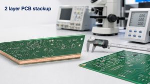
An 2 layer PCB stackup looks simple, but it still affects board thickness, copper weight, routing space, grounding, impedance expectations, assembly yield, and final product fit. For engineers and buyers, the practical question is not only whether a board has two copper layers. It is whether the finished PCB can match the drawing, connector, enclosure, soldering process, and test requirement without avoidable rework.

EBest Circuit (Best Technology) supports 2 layer FR4 PCB fabrication, stackup review, copper thickness confirmation, surface finish selection, SMT assembly, inspection, testing coordination, and small-batch production. If your project already has Gerber files, ODB++, stackup notes, BOM, CPL, drawings, or assembly requirements, please send them to sales@bestpcbs.com for engineering review before production.
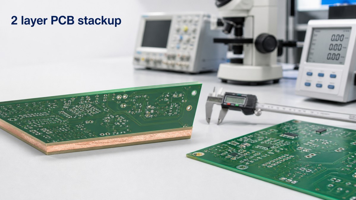
2 layer PCB stackup
A 2 layer PCB stackup should be reviewed together with board thickness, copper weight, routing, and assembly needs.

What Is a 2 Layer PCB Stackup?

A 2 layer PCB stackup is the layer structure of a printed circuit board with one copper layer on the top side and one copper layer on the bottom side. Between the copper layers, the board normally uses an insulating core material such as FR4. Solder mask, silkscreen, and surface finish are then added according to the production requirement.

In everyday quoting, buyers may also call this a double sided PCB, two layer PCB, or 2 layer circuit board. These terms are closely related, but the stackup is the part that tells the manufacturer how the board thickness, copper, dielectric material, and layer arrangement should be built.

A useful 2 layer PCB stackup should make these points clear:

  • finished board thickness, such as 1.6 mm +/-10%;
  • top and bottom copper weight, such as 1 oz or 2 oz;
  • FR4 grade, high-Tg material, or other laminate requirement;
  • surface finish, such as HASL, lead-free HASL, ENIG, OSP, or immersion silver;
  • solder mask color and silkscreen requirement;
  • controlled impedance or special routing notes, if required;
  • SMT, through-hole, panelization, and test requirements.

Standard 2 Layer PCB Stackup Structure

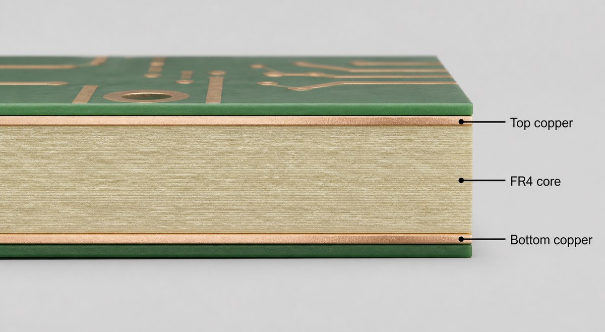
A standard 2 layer PCB stackup is usually built with copper on both sides of an FR4 PCB core. The top layer may carry components, signals, power traces, and local ground copper. The bottom layer may provide additional routing, ground return paths, power routing, and connector connections.
2 layer PCB stackup
A 2 layer PCB usually includes top copper, an FR4 core, and bottom copper, with solder mask and surface finish added during production.
LayerPractical Role
Top solder maskProtects copper and defines solderable openings
Top copperComponents, signals, power, or ground copper
FR4 coreInsulation and mechanical support
Bottom copperRouting, return paths, connectors, or ground copper
Bottom solder maskCopper protection and solder control

The stackup may be simple, but the production result still depends on material availability, copper thickness, finished board thickness, drilling, solder mask registration, surface finish, and panelization. A two layer board should not be treated as a board with no engineering risk.

1.6mm 2 Layer PCB Stackup and Copper Weight

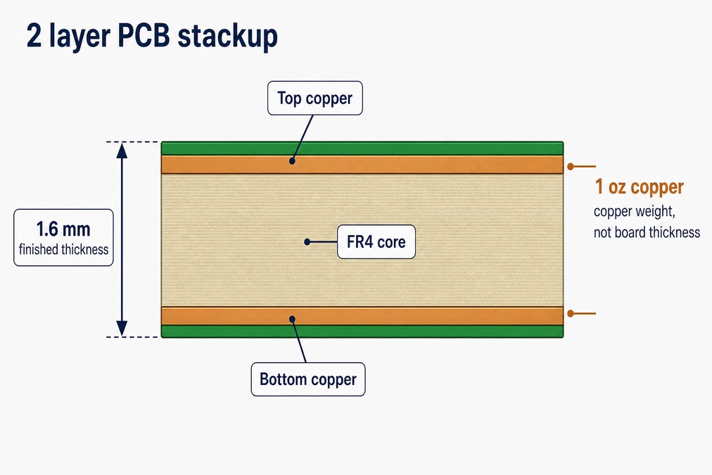
Many 2 layer PCB projects use a 1.6 mm finished board thickness because it is widely supported, mechanically stable, and compatible with many connectors and enclosures. However, 1.6 mm should refer to the finished board thickness, not only the raw laminate thickness.
2 layer PCB stackup
Finished board thickness is measured from the top surface to the bottom surface; copper weight is a separate specification.

Copper weight is a different requirement. For example, 1 oz copper describes the copper thickness or copper weight used on the conductive layers. It does not mean the whole board is 1 oz thick. This distinction matters when a drawing includes both board thickness and copper thickness.

Before production, confirm these thickness-related details:

  • finished board thickness and tolerance;
  • top and bottom copper weight;
  • whether copper is base copper or finished copper;
  • surface finish requirement;
  • connector or enclosure thickness limits;
  • whether impedance or current capacity depends on the stackup.

2 Layer PCB Stackup for Signal, Power, and Ground Routing

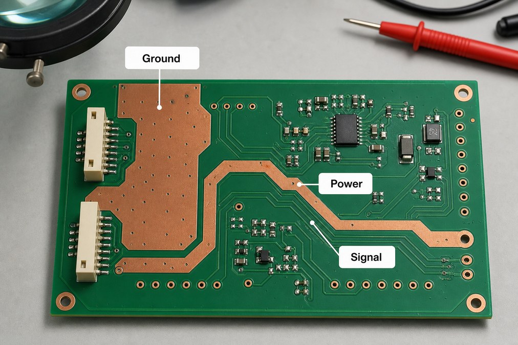
A 2 layer PCB gives less routing freedom than a 4 layer board, so the signal, power, and ground strategy must be practical. If the board has simple low-speed signals, connectors, LEDs, sensors, or basic control circuits, a two layer structure may be enough. If the board has high-speed interfaces, dense BGAs, strict EMI requirements, or multiple power domains, the project may need more review.
2 layer PCB stackup
Signal, power, and ground routing should be planned early on a 2 layer PCB because routing space is limited.

For many 2 layer boards, production review focuses on:

  • return path continuity for important signals;
  • wide enough power traces for current paths;
  • clear ground copper and via stitching where needed;
  • connector orientation and pin mapping;
  • thermal relief, copper balance, and solderability;
  • test points and inspection access after assembly.

The PCB manufacturer should not change the customer’s circuit intent. EBest Circuit can review whether the approved files are manufacturable and whether the stackup, copper, drilling, solder mask, and assembly notes are clear enough before production.

2 Layer PCB Stackup vs 4 Layer PCB Stackup

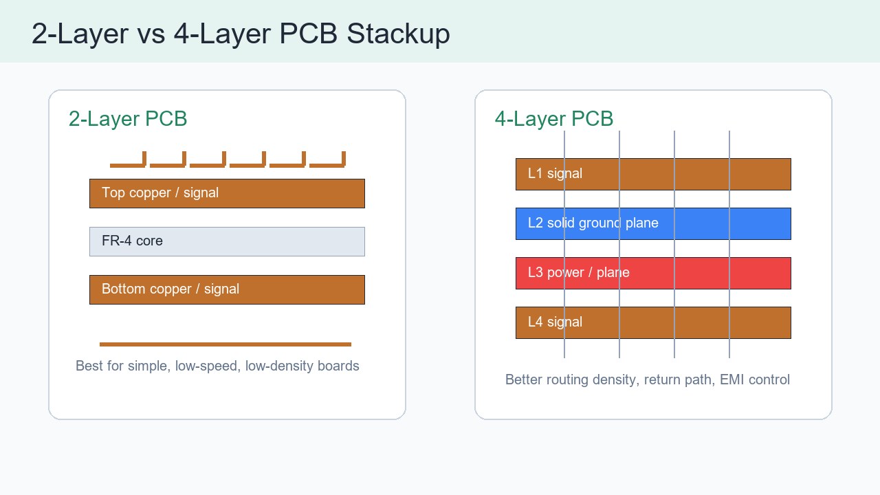
A 2 layer PCB stackup is often a good choice when the project needs a lower-cost board, simple routing, fast prototype validation, or a compact control board without strict high-speed requirements. A 4 layer stackup is usually considered when the board needs better power distribution, cleaner ground reference, controlled impedance, denser routing, or improved EMI behavior.

Item2 Layer PCB4 Layer PCB
Layer structureTop and bottom copperTwo outer layers plus inner planes
Routing spaceLimited but cost-effectiveMore routing freedom
Ground referenceDepends on copper planningUsually stronger with inner plane
CostLowerHigher
Best fitSimple to moderate circuitsDense, faster, or noise-sensitive boards

The right choice depends on the product, not only the layer count. If the 2 layer board can meet routing, grounding, thermal, and assembly needs, it may be the better commercial choice. If the board is already crowded or unstable, moving to 4 layers may save debugging time later.

Manufacturing Checks Before 2 Layer PCB Fabrication

A 2 layer PCB may be easier to manufacture than a high-layer-count board, but file review still matters. A small missing note can lead to wrong thickness, wrong surface finish, solder mask mismatch, connector fit problems, or assembly delay.

EBest Circuit typically checks:

  • Gerber or ODB++ file completeness;
  • drill file and plated-through-hole requirements;
  • finished board thickness and tolerance;
  • copper weight and current-related traces;
  • minimum line width, spacing, annular ring, and solder mask opening;
  • surface finish and solderability requirement;
  • panelization, tooling holes, fiducials, and breakaway method;
  • test requirement and outgoing inspection notes.

This review is useful because the buyer receives a finished PCB, not a file screenshot. The file must be translated into a real board that can be drilled, plated, etched, solder-masked, finished, tested, packed, and assembled.

SMT and PCBA Risks on 2 Layer PCB Boards

If the 2 layer PCB also needs SMT assembly, the stackup should be reviewed together with assembly data. Board thickness, panel size, component placement, solder mask openings, fiducials, and connector positions can all affect SMT yield. If the project also includes component sourcing, the BOM should be checked before SMT scheduling.

Before assembly, the useful files include:

  • Gerber or ODB++ files;
  • BOM with approved part numbers;
  • CPL or pick-and-place file;
  • assembly drawing;
  • polarity and orientation notes;
  • panelization drawing;
  • testing and packing requirements.

For prototype and small-batch PCBA projects, EBest Circuit can review PCB fabrication and SMT assembly together. This helps keep board thickness, panelization, component sourcing, soldering, inspection, and packing notes visible under one workflow. This is especially useful when the project is still in prototype PCB assembly validation.

EBest Circuit 2 Layer PCB Stackup Manufacturing Capabilities

EBest Circuit supports 2 layer FR4 PCB projects from prototype to small-batch and production runs. The practical value is not only making a bare board, but helping the customer confirm the production path before the order moves forward.

RequirementEBest Circuit Support
Board type2 layer FR4 PCB and double sided PCB
Thickness reviewFinished thickness and tolerance confirmation
Copper optionsCommon 1 oz or higher copper review by project
Surface finishHASL, lead-free HASL, ENIG, OSP, and other options
AssemblySMT, through-hole, mixed assembly, and inspection
DocumentsDFM notes, stackup confirmation, test reports when required

EBest Circuit (Best Technology) has worked in PCB and PCBA manufacturing since 2006 and serves customers in more than 40 countries and regions. For customers comparing suppliers, stable engineering communication is often as important as the quote itself, especially when the project needs both PCB fabrication and assembly.

2 Layer PCB Stackup Case Study for a Prototype Build

A USA customer needed a small-batch 2 layer PCB prototype for a compact control board. The board looked simple at first, but the project still had several details that could affect assembly and validation.

Project snapshot:

  • Customer region: USA;
  • Application: compact control and sensor interface board;
  • Quantity: 50 pcs prototype build;
  • PCB type: 2 layer FR4 PCB;
  • Finished thickness: 1.6 mm +/-10%;
  • Copper: 1 oz top and bottom copper;
  • Surface finish: lead-free HASL;
  • Assembly: SMT after PCB fabrication;
  • Delivery focus: prototype validation before the next small batch.

What EBest Circuit reviewed before production:

  • stackup, copper weight, board thickness, and solder mask notes;
  • panelization method for SMT handling;
  • BOM availability and approved part numbers;
  • component polarity, connector direction, and placement data;
  • electrical test before assembly and visual inspection after SMT;
  • single-board packing after assembly to reduce handling damage.

The useful result for the customer was a clearer prototype path. The order quantity was small, but the board still moved through file review, PCB fabrication, SMT preparation, inspection, and packing as one controlled project. That is the kind of support that helps engineering teams validate a 2 layer PCB before scaling the design.

FAQs About 2 Layer PCB Stackup

1. Is a 2 layer PCB stackup the same as a double sided PCB?
In most PCB manufacturing contexts, yes. A double sided PCB usually means a 2 layer PCB with copper on both the top and bottom sides.

2. What is the standard thickness for a 2 layer PCB?
Many 2 layer FR4 boards use 1.6 mm finished thickness, but 0.8 mm, 1.0 mm, 1.2 mm, and other thicknesses may also be used depending on the product.

3. Is 1 oz copper the same as 1.6 mm PCB thickness?
No. 1 oz copper describes the copper layer weight or thickness. 1.6 mm describes the finished board thickness from the top surface to the bottom surface.

4. Can a 2 layer PCB stackup support controlled impedance?
Some 2 layer boards can support impedance requirements, but the stackup, trace width, dielectric thickness, copper thickness, and test requirement should be reviewed before fabrication.

5. What files should I send for a 2 layer PCB quotation?
Send Gerber or ODB++ files, drill files, stackup or thickness notes, BOM, CPL, assembly drawing, surface finish requirement, quantity, test notes, and packing requirements.

All in all, a 2 layer PCB stackup should be clear before production begins. If your project needs 2 layer FR4 PCB fabrication, thickness review, copper confirmation, SMT assembly, or prototype-to-small-batch support, please send your Gerber files, BOM, CPL, drawings, and project notes to sales@bestpcbs.com. EBest Circuit can help review the manufacturing and assembly path before your boards move into production.

You may also like

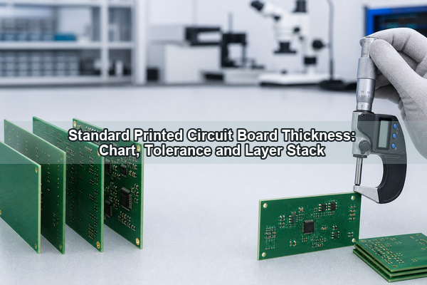
Standard Printed Circuit Board Thickness: Chart, Tolerance and Layer Stack
Thursday, July 30th, 2026

The most common standard printed circuit board thickness is 1.6 mm, approximately 0.062-0.063 inch or 62-63 mil. That value is a practical default for many rigid FR4 boards, but it is not a universal requirement. The correct finished thickness must also fit the layer stack, impedance geometry, connectors, enclosure, assembly process and mechanical load.

Standard printed circuit board thickness samples and dimensional measurement

What Is the Standard Printed Circuit Board Thickness?

For a general-purpose rigid FR4 PCB, 1.6 mm is the conventional nominal finished thickness. The number developed from the older 1/16-inch laminate format, which equals 1.5875 mm. Modern fabrication drawings may state 1.57 mm, 1.60 mm, 0.062 inch or 0.063 inch, depending on the drawing convention and the fabricator’s standard material system.

“Standard” means commonly stocked and routinely processed, not mandatory. A compact sensor module can use 0.8 mm to reduce height. A card-edge board may need 1.6 mm to fit its connector. A large industrial board may use 2.0 mm or 2.4 mm for stiffness. The stated value should therefore be treated as the nominal finished board thickness, with a separate tolerance that defines the acceptable production range.

Standard PCB Thickness Chart in Millimeters, Inches and Mils

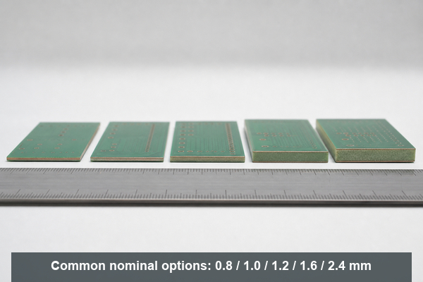
The chart below converts common rigid-board thickness options. Availability varies with laminate family, layer count, copper weight and the fabricator’s stocked constructions.

Nominal Thickness Approx. Inches Approx. Mils Typical Design Direction
0.4 mm 0.016 in 16 mil Very thin rigid modules and space-limited assemblies
0.6 mm 0.024 in 24 mil Compact modules with controlled mechanical support
0.8 mm 0.031 in 31 mil Thin consumer, handheld and daughterboard designs
1.0 mm 0.039 in 39 mil Low-profile rigid boards with moderate stiffness
1.2 mm 0.047 in 47 mil Space-saving multilayer and control boards
1.6 mm 0.063 in 63 mil General rigid PCB default
2.0 mm 0.079 in 79 mil Boards needing additional stiffness or stackup space
2.4 mm 0.094 in 94 mil Industrial, connector or multilayer mechanical requirements
3.2 mm 0.126 in 126 mil Thick rigid boards and demanding mechanical structures

These are nominal values rather than guaranteed measurements. The finished board is accepted against the thickness tolerance on the fabrication drawing. Conversion is also approximate because 1 mil equals 0.001 inch, while metric laminate systems are usually specified directly in millimeters.

Standard PCB thickness chart with common rigid board samples

Why Is 1.6 mm the Most Common PCB Thickness?

The 1.6 mm format remains common because material supply, fabrication tooling, connector geometry and product mechanics developed around the former 1/16-inch standard. It provides enough rigidity for many board sizes without making the assembly unnecessarily heavy. Fabricators can also build a wide range of 2-layer and multilayer constructions around this finished target.

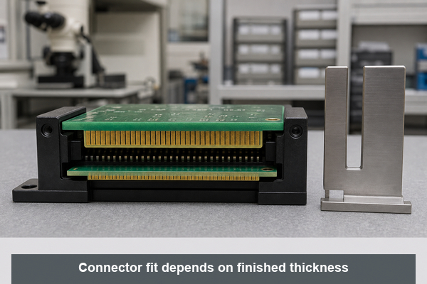
Component compatibility is another reason. Many card-edge connectors, board guides, standoffs and through-hole leads are designed around boards close to 1.6 mm. Using a thinner or thicker board can still be correct, but the mechanical interface must be checked rather than assumed. Press-fit hardware is especially sensitive because hole geometry, board thickness and pin engagement work together.

Cost is usually predictable at 1.6 mm because common cores and prepregs are readily available. A different thickness does not automatically make a PCB expensive, but a non-stock laminate construction, an unusual tolerance or a difficult multilayer build can require additional engineering and process control.

How Does PCB Thickness Differ From Copper Thickness?

PCB thickness is the total finished board thickness. Copper thickness describes the conductor thickness on an individual layer. They are related in the stackup, but they are not interchangeable specifications.

Specification What It Measures Common Units Main Design Effects
Finished board thickness Total rigid PCB construction mm, inch, mil Mechanical fit, stiffness, stackup space and drilling aspect ratio
Copper thickness Copper on one conductor layer oz/ft², µm, mil Current capacity, trace resistance, etching and spacing
Dielectric thickness Insulation between selected copper layers mm, µm, mil Impedance, coupling, isolation and layer spacing

Typical nominal foil conversions are approximately 17 µm for 0.5 oz, 35 µm for 1 oz and 70 µm for 2 oz copper. Outer-layer finished copper may differ from starting foil because hole plating and pattern plating add copper. A 1.6 mm board can therefore use different copper weights without ceasing to be a 1.6 mm nominal board, provided the dielectric construction is adjusted accordingly.

A thick PCB is also not automatically a heavy-copper PCB. A 2.4 mm board with 1 oz copper is mechanically thick but does not use heavy copper. A 1.6 mm board with 4 oz copper is a heavy-copper design even though its total board thickness is conventional. The thick PCB board guide addresses the manufacturing effects of unusually thick rigid constructions.

What Determines Finished PCB Thickness?

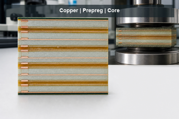
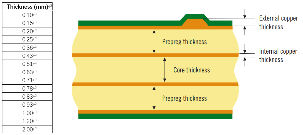
Finished thickness is created by the complete pressed stack, not by one laminate sheet. A 2-layer board may use a copper-clad core and solder mask. A multilayer board combines etched cores, prepreg bonding layers, outer copper, plating and surface coatings. Press temperature, pressure, resin flow and copper distribution affect the result.

  • Core thickness: defines much of the rigid dielectric structure and provides copper on one or both sides.
  • Prepreg type and count: determine bonding thickness after resin flows into copper features and cures.
  • Copper weight: changes the conductor height and the volume of resin needed to fill around traces and planes.
  • Layer count: adds copper and dielectric interfaces, increasing the number of variables in the pressed stack.
  • Plating and finish: add smaller local thickness contributions, especially on outer copper and hole walls.
  • Material system: affects resin content, glass style, pressed thickness, thermal expansion and availability.

Prepreg should not be treated as a fixed spacer before lamination. Its final thickness depends on glass style, resin content, copper pattern density and the press cycle. For controlled builds, the fabricator models the pressed result and selects a balanced set of cores and prepregs. A PCB thickness calculator can support an early estimate, but it cannot replace the production stackup.

Multilayer PCB stackup showing core prepreg copper and finished thickness

How Thick Are 2-, 4-, 6-, 8-, 12- and 32-Layer PCBs?

Layer count does not assign one compulsory board thickness. The finished value depends on routing density, copper weight, dielectric spacing, via structure and mechanical requirements. The following ranges are practical starting points for rigid FR4 discussions, not universal standards.

Layer Count Common Starting Thicknesses Important Constraint
2 layers 0.8, 1.0, 1.2 or 1.6 mm Core thickness usually dominates the construction
4 layers 1.0, 1.2 or 1.6 mm Plane spacing and outer copper affect the final build
6 layers 1.2, 1.6 or 2.0 mm More dielectric interfaces must fit the impedance plan
8 layers 1.6, 2.0 or 2.4 mm Routing density and via aspect ratio become more influential
12 layers 1.6, 2.0, 2.4 or 3.2 mm Thin dielectrics or HDI may be needed to limit total thickness
32 layers Custom multilayer construction No universal value; lamination, drilling and reliability govern the build

A 4-layer PCB can be 0.8 mm or 2.0 mm, and a 12-layer PCB can sometimes remain near 1.6 mm by using thin cores and prepregs. That does not mean the thinnest possible build is best. Very thin dielectrics can increase coupling, demand tighter registration and make resin filling more difficult. Very thick builds can increase plated-hole aspect ratio and create longer via stubs.

The layer structure should be selected before the board outline and mechanical system are frozen. The related 4 layer vs 2 layer PCB comparison explains how the extra planes change routing and EMC behavior; thickness remains a separate, coordinated decision.

How Does PCB Thickness Affect Impedance and Signal Integrity?

Total board thickness affects the available stackup space, but controlled impedance is governed by the local transmission-line geometry. Trace width, copper thickness, dielectric thickness, dielectric constant, solder mask and reference-plane relationship determine the impedance of a microstrip or stripline.

Changing a 1.6 mm board to 1.2 mm does not automatically change every trace impedance. If the relevant dielectric spacing and material properties remain the same, some signal layers may retain their geometry. In practice, however, reducing total thickness often forces changes to cores and prepregs, so the impedance model must be recalculated.

Thicker boards can also produce longer through-vias and longer unused via stubs. At higher data rates, those stubs may create resonances and insertion-loss problems. Backdrilling, blind vias or a different layer assignment may be needed. A production impedance control PCB therefore links the trace model to the confirmed laminate construction and measured impedance coupons.

How Does PCB Thickness Affect Mechanical Fit and Connector Compatibility?

Mechanical interfaces often set a harder thickness limit than the electrical circuit. Card-edge connectors specify an acceptable board-thickness range so their contacts apply the intended normal force. Board guides, slots, bezels, standoffs and enclosures also have limited clearance. A nominal change of a few tenths of a millimeter can affect insertion, alignment or screw loading.

  • Confirm card-edge connector slot width and contact engagement.
  • Check press-fit pin length, compliant-zone position and supported board range.
  • Verify standoff height, enclosure gaps and component clearance.
  • Review board span, mounting-hole spacing and bending load.
  • Include finished-thickness tolerance in the mechanical stack analysis.

Thin boards may need additional support during insertion or handling. Thick boards provide stiffness but increase weight and can move component terminals relative to the enclosure. The mechanical drawing should therefore use the full allowed thickness range, not only the nominal value.

PCB thickness effect on card edge connector and enclosure fit

How Does PCB Thickness Influence Warpage, Assembly and Reliability?

Board thickness contributes to bending stiffness, but warpage depends on material modulus, copper balance, stack symmetry, moisture, temperature and panel design. A thin board is more easily deflected by handling, component weight and reflow fixtures. A thick asymmetric board can still warp if copper and dielectric structures are poorly balanced.

During soldering, the PCB experiences a temperature gradient while copper, glass and resin expand at different rates. Large copper areas on one side, uneven component mass or an unbalanced stack can create bow and twist. The board warpage guide explains how stack symmetry, copper distribution, panel support and reflow conditions work together.

Assembly equipment also has practical limits. Very thin boards may require carriers for solder-paste printing, placement and reflow. Very thick boards have greater thermal mass and may need a profile that heats solder joints adequately without overstressing components. Depanelization, connector insertion and functional-test fixtures must use forces that do not bend or crack the finished assembly.

What Is PCB Thickness Tolerance and How Is It Measured?

PCB thickness tolerance is the permitted difference between nominal and actual finished thickness. A commercial rigid FR4 build commonly uses a percentage tolerance such as ±10%, but the actual requirement must be confirmed for the material, thickness and construction. A 1.6 mm board with ±10% tolerance has an acceptance range of 1.44-1.76 mm.

Tighter tolerance may be justified for card-edge contacts, press-fit components, controlled mechanical gaps or precision fixtures. It can require a more restricted material set and closer process control. The drawing should state the nominal value, tolerance and whether the measurement includes solder mask when that distinction is mechanically significant.

Finished boards are commonly checked with a calibrated micrometer or thickness gauge. Measurements should be taken at defined locations, away from edge burrs, local copper buildup or surface contamination. Multiple points reveal thickness variation across the panel. Cross-section analysis is used when the individual core, prepreg, copper or plating contributions must be verified rather than only the total board thickness.

PCB finished thickness measurement using a calibrated micrometer

When Should You Use a Thin or Thick PCB?

Use a thinner rigid PCB when product height and weight are constrained, the board is mechanically supported and the stackup can still meet impedance, insulation and assembly requirements. Common thin choices include 0.6, 0.8, 1.0 and 1.2 mm. An extra thin PCB needs more attention to handling, panel support, drilling and warpage than a conventional 1.6 mm board.

Use a thicker PCB when the structure needs greater stiffness, the layer stack needs more dielectric space, the board spans a large unsupported area or a connector system requires a specific engagement depth. Common thicker choices include 2.0, 2.4 and 3.2 mm. Thickness alone does not improve current capacity or thermal performance; copper geometry, material properties and the complete heat path still control those functions.

Keep 1.6 mm when it satisfies all electrical and mechanical constraints. It is usually the lowest-risk starting point because materials, assembly fixtures and connector ecosystems are widely compatible with it. Move away from that value only for a defined reason, then validate the linked stackup and mechanical changes.

How Should Finished Thickness Be Defined in PCB Documentation?

Gerber or ODB++ image data defines conductor, mask and legend geometry, but it does not reliably define the required finished board thickness. The value belongs in the fabrication drawing, manufacturing notes or an approved stackup table. The same controlled document should identify the unit and tolerance.

For a simple 2-layer board, a note such as “Finished board thickness: 1.60 mm ±10%” can be sufficient when no special stack construction is required. A controlled-impedance multilayer board needs an approved stackup showing layer order, copper weight, material family, core and prepreg construction, dielectric targets and finished thickness. Mechanically critical designs should also identify connector or press-fit constraints so the allowed range is consistent across drawings.

Revision control matters because changing finished thickness can alter enclosure fit, impedance geometry, via aspect ratio, test fixtures and assembly support. A thickness change should therefore trigger review of the stackup and mechanical interfaces instead of being treated as an isolated fabrication option.

FAQ About Standard Printed Circuit Board Thickness

Is 1.6 mm the only standard PCB thickness?

No. It is the most common rigid FR4 value, but 0.4, 0.6, 0.8, 1.0, 1.2, 2.0, 2.4 and 3.2 mm are also regularly used when the stackup and product mechanics support them.

How thick is a 2-layer PCB board?

A 2-layer rigid PCB is often 1.6 mm, but 0.8, 1.0 and 1.2 mm are common for compact products. The copper-clad core usually contributes most of the finished thickness.

How thick is a 4-layer PCB?

Many 4-layer PCBs use 1.6 mm, while 0.8, 1.0, 1.2 and 2.0 mm are possible. The selected cores and prepregs must provide the required plane spacing and impedance geometry.

Does a 12-layer PCB have to be thicker than 1.6 mm?

No. Some 12-layer constructions can fit within 1.6 mm by using thin dielectrics. Other designs need 2.0, 2.4 or 3.2 mm for routing, isolation, copper or via requirements.

Does thicker PCB material carry more current?

Not by itself. Current capacity depends mainly on copper thickness, trace or plane geometry, allowed temperature rise, airflow and the complete thermal path.

Can a PCB thickness calculator define the production stackup?

A calculator can estimate total thickness, but production values depend on pressed prepreg thickness, copper pattern, material data and lamination behavior. The fabricator’s confirmed stackup is the final reference.

Is solder mask included in finished PCB thickness?

Practices can differ. Solder mask contributes only a small amount, but mechanically critical drawings should state whether the specified finished thickness includes mask and where measurement is taken.

What tolerance is common for a 1.6 mm PCB?

±10% is a common commercial reference, corresponding to 1.44-1.76 mm, but the applicable tolerance depends on the material and construction and must be stated on the drawing.

Conclusion

Standard printed circuit board thickness is commonly 1.6 mm, but that default is only correct when the layer stack, impedance, connector, enclosure, assembly and tolerance requirements agree with it. A sound design separates total board thickness from copper thickness, defines the finished value in controlled documentation and verifies the actual production range.

EBest Circuit (Best Technology) manufactures rigid FR4 boards from very thin 2-layer constructions through thick multilayer builds, subject to material, stackup, dimensions and engineering review. For technical support on a thickness-sensitive PCB design, contact sales@bestpcbs.com.

You may also like

4 Layer vs 2 Layer PCB
Tuesday, July 7th, 2026

A 2 layer PCB is usually the right choice for simple, low-speed, low-density circuits where bare-board cost matters most. A 4 layer PCB is usually the better choice when the design needs cleaner return paths, better EMI control, easier routing, stronger power distribution, or more reliable high-speed behavior.

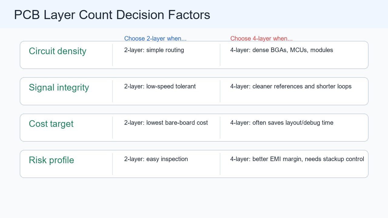
The practical decision is not only “two layers are cheaper” or “four layers are better.” The best layer count depends on circuit density, signal edge speed, power integrity, board size, EMC risk, connector placement, assembly yield, and the cost of redesign if the first prototype fails.

Side by side stackup comparison of a 2 layer PCB and a 4 layer PCB
2 layer and 4 layer PCB stackups differ most in routing space, plane structure, and return-current control.

Quick Answer: Choose 2 Layer for Simplicity, 4 Layer for Performance Margin

Choose a 2 layer PCB when the circuit is simple enough to route cleanly without cutting the ground path. Choose a 4 layer PCB when the board needs continuous reference planes, dense routing, lower loop area, or better control of EMI and signal integrity.

Decision Factor 2 Layer PCB 4 Layer PCB Engineering Note
Best fit Simple control boards, LED boards, basic power boards, low-speed sensors MCU boards, wireless products, mixed-signal boards, compact electronics Layer count should follow routing and noise risk, not habit.
Routing density Limited to top and bottom copper Outer routing plus inner reference and power planes 4 layers often reduce routing compromises.
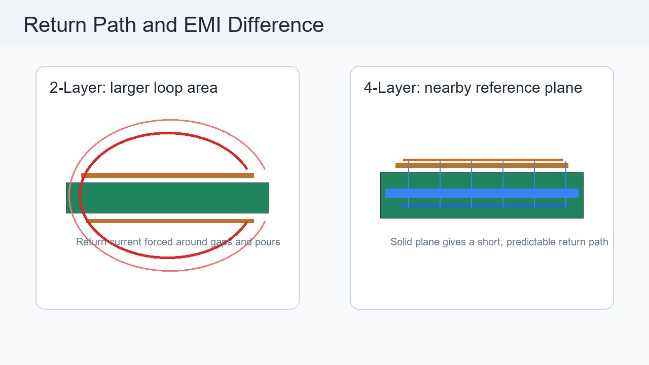
EMI control Depends heavily on layout discipline and ground pours Easier to maintain short return paths with a solid plane Continuous reference planes reduce loop area.
Cost Lower bare-board cost Higher bare-board cost, sometimes lower debug cost For dense designs, 4 layers may save engineering time.
Manufacturing risk Easy to inspect and fabricate Needs stackup control, lamination, and clearer documentation Ask for stackup, impedance, and inspection requirements early.

What Is a 2 Layer PCB?

A 2 layer PCB has copper on the top and bottom sides of the board, separated by an insulating core. It can route signals on both sides, use vias to change layers, and use copper pours for ground or power distribution.

Two-layer boards are common in basic industrial controls, small LED products, simple power distribution, connector adapters, low-speed sensor boards, and cost-sensitive prototypes. The main limitation is that every trace, via, connector, and copper pour competes for the same two copper layers.

What Is a 4 Layer PCB?

A 4 layer PCB has four copper layers separated by dielectric material. A common structure is top signal, inner ground plane, inner power plane, and bottom signal, although the best stackup should be confirmed with the PCB manufacturer and the design requirements.

The main advantage is not only “more routing layers.” A 4 layer PCB can place signal traces close to a continuous reference plane, which gives return current a predictable path and helps reduce radiation, crosstalk, and ground bounce. This is why many compact digital products start at four layers even when the schematic looks moderate.

2 Layer vs 4 Layer PCB Stackup Differences

The biggest stackup difference is that a 4 layer board can dedicate inner copper to planes, while a 2 layer board must share copper for signals, power, and ground. That changes the way current returns, how decoupling capacitors behave, and how easily the layout can pass EMC testing.

Stackup Item 2 Layer PCB 4 Layer PCB Buyer or Engineering Note
Typical layers Top copper and bottom copper Top signal, ground plane, power or plane layer, bottom signal Actual construction varies by supplier and thickness.
Reference plane Ground pour may be interrupted by routing Solid inner ground plane is practical Ask whether critical signals cross plane splits or voids.
Power distribution Wider traces or pours are needed Power plane or large inner copper can reduce impedance High-current boards still need thermal and copper-width checks.
Impedance control Harder and less predictable More practical with controlled dielectric and planes Request impedance coupon and stackup data when required.
Board thickness Often simple standard thickness Needs defined dielectric and copper arrangement Confirm finished thickness, copper weight, and tolerance.

When a 2 Layer PCB Is the Better Choice

A 2 layer PCB is better when the circuit can be routed with clean grounding, enough spacing, and no high-speed or EMI-critical constraints. It is also attractive when the product needs a simple bare board, a low prototype cost, or very easy visual inspection.

  • The board has low-speed digital signals, simple analog paths, or basic switching.
  • The board size is not tightly constrained, so wider traces and ground pours fit.
  • The product is cost-sensitive and does not need controlled impedance.
  • The design has low component density and no fine-pitch BGA or dense connector field.
  • The EMC environment is mild and the enclosure, cable, and power system are simple.

A good 2 layer design still needs disciplined grounding. Avoid narrow ground traces, long return loops, poor decoupling placement, and random copper islands that look like ground but do not provide a reliable return path.

When a 4 Layer PCB Is the Better Choice

A 4 layer PCB is better when the board needs routing freedom and electrical margin. The additional layers help the designer maintain a continuous reference plane, route around dense components, and separate power distribution from sensitive signal paths.

  • The board includes fast digital edges, USB, Ethernet, RF modules, DDR, high-speed ADCs, or dense MCU routing.
  • Ground return paths are broken or difficult to control on a 2 layer layout.
  • The product must reduce EMI risk before compliance testing.
  • The PCB must be compact, connector-heavy, or packed with fine-pitch components.
  • The design needs a stable power distribution network and better decoupling behavior.

For many commercial products, 4 layers are used because the extra bare-board cost is smaller than the risk of a failed EMC test, unstable prototype, or repeated layout cycle.

Decision factors for choosing between a 2 layer PCB and a 4 layer PCB
Layer count selection should compare circuit density, signal integrity, cost target, and project risk together.

Cost Difference: Bare Board Price vs Total Project Cost

A 2 layer PCB usually has the lower bare-board price, but a 4 layer PCB can lower total project cost when it prevents redesign, noise troubleshooting, or EMC failure. Procurement should compare the full cost of the design decision, not only the first PCB quotation.

Cost Area 2 Layer PCB Impact 4 Layer PCB Impact What to Check Before Ordering
Bare PCB fabrication Usually lower Usually higher due to lamination and extra copper layers Compare quantity, size, copper weight, finish, and delivery time.
Layout time Can increase if routing is congested Often easier for dense boards Ask whether the designer is forcing a 2 layer board too far.
EMI debugging Higher risk on noisy or cable-connected products Lower risk when planes and decoupling are designed well Consider EMC test cost and project schedule impact.
Assembly yield Good for simple boards Good when routing supports clean placement and test access Check test points, panelization, and soldering access.
Future revisions May need a layer-count upgrade later More margin for product updates Consider whether the product roadmap adds functions.

Signal Integrity and EMI: Why Ground Planes Matter

Signal integrity and EMI are often the reason a design moves from 2 layers to 4 layers. A solid ground plane under signal traces gives return current a short path, reduces loop area, and helps contain electromagnetic fields.

On a 2 layer board, ground pours can help, but they are frequently cut by routing channels, vias, slots, connectors, and power traces. When the return path has to detour, the loop area grows. Larger loops are more likely to radiate noise and pick up noise from nearby switching circuits.

Return path and EMI comparison between 2 layer and 4 layer PCB layouts
A 4 layer PCB can keep signal traces close to a continuous reference plane, reducing loop area and EMI risk.

Routing Density and Component Placement

A 4 layer PCB makes routing easier when components are dense, but it does not replace good placement. Put connectors, power sections, clocks, high-current paths, and sensitive analog areas in logical zones before deciding whether two layers are enough.

For a 2 layer design, routing congestion often causes long traces, extra vias, narrow ground necks, and poor test-point access. For a 4 layer design, routing can be cleaner, but the designer must still avoid plane splits under critical signals and document which layers are used for reference and power.

Manufacturing and Quality Control Differences

A 2 layer PCB is simpler to fabricate, while a 4 layer PCB needs tighter control of lamination, registration, dielectric thickness, and stackup documentation. This does not make 4 layer boards risky, but it does mean the supplier should receive clearer fabrication notes.

  • Confirm finished thickness, copper weight, solder mask, surface finish, and impedance requirements.
  • For 4 layer boards, request the stackup before fabrication if impedance, EMI, or mechanical thickness matters.
  • Use IPC-A-600 and IPC-6012 acceptance class requirements when they are part of the buyer’s quality specification.
  • Check annular ring, drill tolerance, minimum trace/space, solder mask bridge, and via fill or tenting requirements.
  • Keep test points accessible, especially when the 4 layer design is dense and assembled with fine-pitch parts.

Common Mistakes When Choosing Layer Count

The most common mistake is choosing the layer count by price alone. Another common mistake is assuming that a 4 layer PCB automatically fixes EMI, even when the stackup has poor reference planes or signals cross plane gaps.

Mistake Why It Matters Better Decision
Forcing dense routing onto 2 layers Creates long traces, broken ground paths, and hard-to-debug noise Compare 4 layer cost against redesign and EMC risk.
Using 4 layers without a clear stackup Planes may not support the signals that need them Define layer order, reference plane, and dielectric targets.
Ignoring power return paths High-current loops can heat copper and radiate noise Review power width, copper weight, via count, and thermal path.
Comparing quotes with different specs Price differences may come from finish, copper, test, or delivery Use the same Gerber, stackup, quantity, finish, and test requirements.
Skipping DFM review Small layout problems can become production defects Ask the PCB supplier for DFM feedback before mass production.

Procurement Checklist Before Ordering 2 Layer or 4 Layer PCB

Procurement should ask technical questions before comparing price, because layer count affects quality requirements, lead time, and manufacturing control. A clear RFQ reduces quotation errors and avoids surprise engineering changes.

  • What is the finished board thickness and tolerance?
  • What copper weight is required on outer and inner layers?
  • Does the design require controlled impedance or impedance testing?
  • What minimum trace/space, drill size, annular ring, and solder mask bridge are used?
  • Is electrical test required for every board?
  • Are there high-current, RF, high-speed, or mixed-signal areas that need engineering review?
  • Does the supplier provide DFM feedback before production?
  • For 4 layer PCB, can the supplier confirm the proposed stackup before fabrication?

Best Practical Selection Rule

The best rule is to use 2 layers only when the board remains electrically clean, manufacturable, and easy to test. Use 4 layers when the design needs a controlled reference plane, better routing density, or more performance margin than a 2 layer layout can provide.

For early prototypes, a 2 layer board may be enough to validate a simple circuit. For products with cables, switching power, fast digital interfaces, dense modules, or EMC exposure, starting with 4 layers often produces a cleaner design path.

FAQ About 4 Layer vs 2 Layer PCB

Is a 4 layer PCB always better than a 2 layer PCB?

No. A 4 layer PCB is usually better for dense routing, EMI control, and signal integrity, but a 2 layer PCB can be the better choice for simple, low-speed, cost-sensitive designs.

When should I upgrade from 2 layer to 4 layer PCB?

Upgrade when routing is congested, return paths are broken, EMI risk is high, impedance control is needed, or the board includes dense ICs, fast edges, wireless modules, or mixed-signal sections.

Is a 4 layer PCB much more expensive?

It is usually more expensive as a bare PCB because it needs more copper layers and lamination. However, the total project cost can be lower if 4 layers reduce redesign, EMI debugging, or layout time.

Can a 2 layer PCB pass EMI testing?

Yes, many 2 layer boards can pass EMI testing when the layout, grounding, filtering, enclosure, and cable design are well controlled. The risk rises when the board has fast edges, switching power, long cables, or broken return paths.

What is the common 4 layer PCB stackup?

A common stackup is signal, ground plane, power plane, and signal. Some designs use two ground reference layers or different plane arrangements. The right stackup should be confirmed with the manufacturer and the design requirements.

Is a 2 layer PCB suitable for LED products?

Often yes. Simple LED boards can use 2 layers when current, heat, copper width, and voltage drop are controlled. High-power LED boards may need heavier copper, metal-core PCB, or special thermal design instead of simply adding layers.

Does a 4 layer PCB improve heat dissipation?

It can help spread heat when inner copper planes are designed as part of the thermal path, but layer count alone is not a thermal solution. Copper weight, via arrays, board material, component placement, and enclosure contact matter more.
Can I route high-speed signals on a 2 layer PCB?

Some moderate-speed designs can work on 2 layers, but high-speed signals become harder to control because the return path and impedance are less predictable. For reliable high-speed interfaces, 4 layers are usually a safer starting point.

Do I need controlled impedance for every 4 layer PCB?

No. Controlled impedance is needed when the interface or signal speed requires it. If needed, specify impedance values, tolerance, layer reference, stackup, and test requirements in the fabrication notes.

Which is better for prototypes, 2 layer or 4 layer PCB?

Use 2 layers for simple proof-of-concept prototypes where cost and speed matter. Use 4 layers when the prototype must represent real EMI, signal integrity, power integrity, and product-size constraints.

Can a 4 layer PCB make assembly harder?

Layer count itself does not usually make assembly harder, but dense 4 layer layouts may reduce test access and increase placement complexity. Keep test points, fiducials, panelization, and soldering clearance in the DFM review.

What should I send to a supplier for a 4 layer PCB quote?

Send Gerber files, drill files, BOM if assembly is required, stackup requirements, finished thickness, copper weight, surface finish, impedance requirements, solder mask color, quantity, test requirements, and delivery expectations.

Final Recommendation

For a simple low-speed board, 2 layers can be the most economical and practical choice. For dense electronics, high-speed interfaces, EMI-sensitive products, compact layouts, or production designs where failure is expensive, 4 layers usually provide better engineering margin.

If you’re sourcing reliable PCB/PCBA manufacturing, including OEM, ODM, prototyping, mass production, or custom engineering solutions, reach out to our engineering team for technical support and a quote at sales@bestpcbs.com.

You may also like

PCB Stack-up and Impedance Control Guidelines
Friday, August 23rd, 2024

When designing a PCB board, careful attention to stack-up and impedance control is essential for achieving optimal signal integrity and performance. The PCB stack-up refers to the arrangement of copper and insulating layers that make up the board. Impedance control, on the other hand, involves maintaining consistent electrical characteristics within signal traces, especially in high-speed circuits. This post provide a detailed guideline of PCB stack-up and impedance control for designers.

PCB Stack-up Parameter

Internal Copper Thickness After Processing

Base FoilMin. After Processing
18um (1/2oz)11.4um
35um (1oz)24.9um
70um (2oz)55.7um
105um (3oz)86.6um
140um (4oz)117.5um

External Copper Thickness After Plating

Base FoilMin. Class 2Min. Class 3
12um (3/8oz)29.3um34.3um
18um (1/2oz)33.4um38.4um
35um (1oz)47.9um52.9um
70um (2oz)78.7um83.7um
105um (3oz)108.6um113.6um
140um (4oz)139.5um144.5um

Common Prepreg (PP) Properties

TypeThickness (mm)Resin (%)
1060.0565
10800.07565
21160.1255
76280.246

Common Material List

Medium TgShengyi S1000-H
ITEQ IT-158
Elite EMC-825
High TgShengyi S1000-2M
ITEQ IT-180A
Elite EMS-827

Common Core Thickness

PCB Stack-up and Impedance Control Guidelines

Design Tips – Stack-up

1. Ensure the stack-up remains symmetric.

2. Typically, a foil build is recommended. Special core builds, like those with Rogers, are possible but less common.
3. For boards thicker than 1mm, the standard thickness tolerance is +/-10%. For 1mm boards, the standard tolerance is +/-0.1mm. Any board with a thickness ≤1mm requires approval from Best Tech.

4. The minimum dielectric thickness will be 90µm, according to IPC standards, unless otherwise specified by the FAB drawing and there are no micro vias.

5. Use a maximum of three sheets of prepreg to bond the layers.

6. While the stack-up used in production may differ slightly from the specified one, an Engineering Query (EQ) will be sent for confirmation.

7. Variations can occur due to factors like copper distribution and available materials.
8. Thicker copper foils require thicker dielectrics between layers, and the foil thickness after processing differs from the base foil thickness.

9. Additionally, variations in resin percentage for the same prepreg type can impact the final prepreg thickness.

10. When incorporating micro vias, consider the aspect ratio—recommended at 0.8:1 and advanced at 1:1—when selecting prepreg.

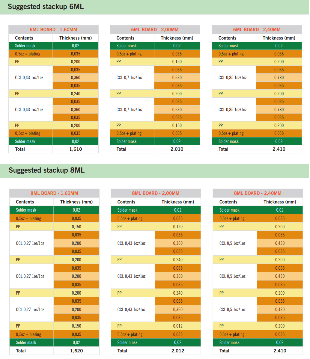
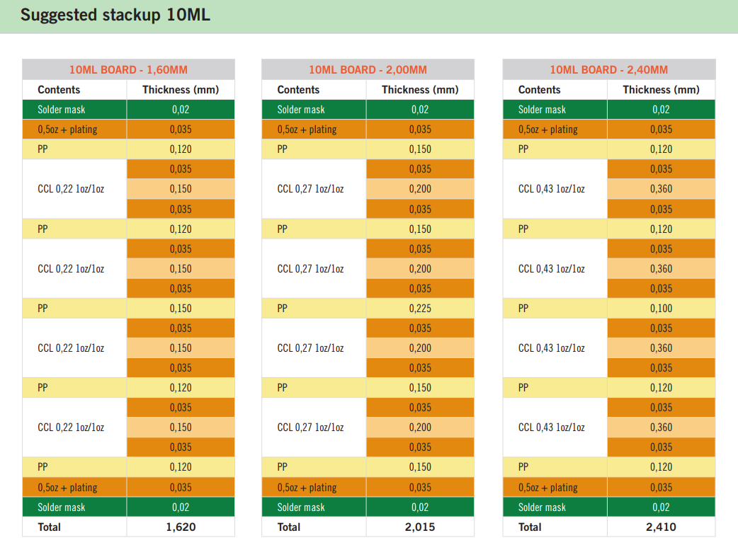
If you need special materials, thickness tolerances, or stack-ups, contact EBest Circuit (Best Technology) for guidance. Below are some suggested stack-ups for different layers PCB.

PCB Stack-up and Impedance Control Guidelines

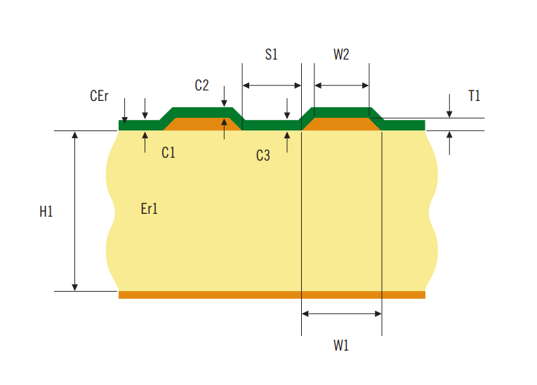
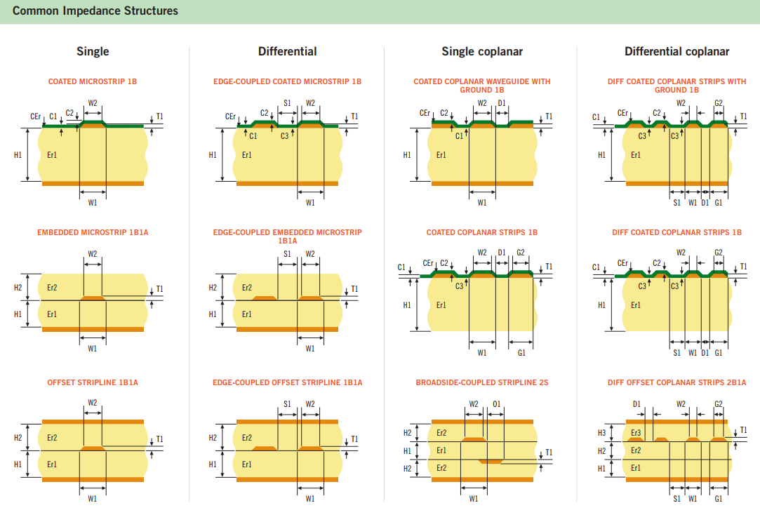
Impedance Parameters Needed for Calculation

PCB Stack-up and Impedance Control Guidelines
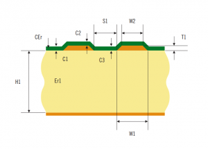
SymbolFeature
H1, H2, H3..Dielectric thickness between copper layers after pressing
Er1Dielectric constant of prepreg or core used between copper layers.
W1The bottom width od impedance lines, which is the customer required impedance trace width.
W2The top width of impedance lines.
S1The space between two differential impedance traces.
T1Finished copper thickness, which is different with our normal definition.
C1Solder mask thickness on material.
C2Solder mask thickness on copper.
C3Solder mask thickness on material between traces (C1 = C3).
CErDielectric constant of solder mask. Normally use 3.4 to calculate.

Tolerance of Impedance Control

Type of ImpedanceCommon Requested ValueTolerance of Impedance Control
GeneralModerateAdvanced
Single/Single Coplanar        40Ω/510Ω/75Ω+/-10%+/-8%+/-5%
Differential/Differential Coplanar90Ω/100Ω/120Ω+/-10%+/-8%+/-5%

Relationship between Parameters and Impedance Value

Parameters ModificationEffect on Impedance Value
ParametersIncrease/ReduceImpacts on impedanceImpedance value increase/reduced
H (dielectric thickness)IncreaseBigIncrease
W (trace width)IncreaseBigReduced
S (trace space)IncreaseBigIncrease
T (copper thickness)IncreaseLowReduced
C (solder mask thickness)IncreaseLowReduced

Design tips – Impedance

When signal speeds exceed 2 GHz and timing is critical, consider using better materials such as medium, high, or ultra-high-speed options, along with flat glass styles. To ensure a reliable lamination process and prevent resin starvation, allow the factory to select the number of prepregs, prepreg styles, and resin content in the stack-up.

Key factors influencing impedance signal losses include:

1. Line Length: Signal losses are directly proportional to the line length—shorter lines result in fewer losses, while longer lines lead to greater losses.

2. Dielectric Loss: These losses can be minimized by selecting appropriate materials.

3. Copper Loss: This includes losses from the cross-sectional area (affected by stack-up design) and surface roughness, which can be reduced through material selection and proper stack-up configuration.

If you require impedance tolerances tighter than +/-10%, discuss your design possibilities with the EBest Circuit (Best Technology) team.

When designing rigid-flex boards, note that separate calculations are necessary for both the rigid and flex sections of the same signal. Manufacturers will adjust the thickness and dielectric constant of the solder mask based on their solder mask properties and printing method. Variations in resin content for the same prepreg type can also affect impedance. For assistance with impedance calculations, contact EBest Circuit (Best Technology) for support.

PCB Stack-up and Impedance Control Guidelines

Checklist of Necessary Information for Impedance Calculations

1. Specify the type, value, and tolerance of impedance control.

2. Ensure you define the width and space of impedance traces, as well as the layers where these traces will be present, along with the layers to be considered as reference points.

3. Identify the type of material and final board thickness, and provide a reference stack-up for the design.

4. Confirm the finished copper thickness on external and internal layers, and note if any special type of solder mask is required.

5. Always request EBest Circuit (Best Technology)’s stack-up before starting the routing design.

You may also like