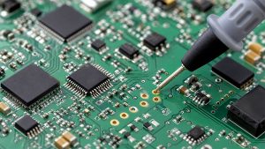
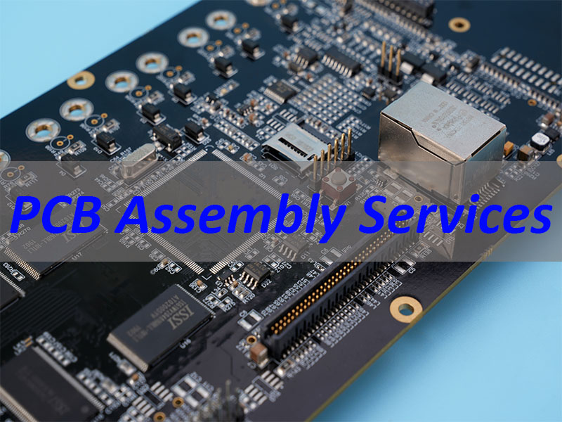
PCB assembly services cover the full process of turning bare printed circuit boards into tested, functional electronic assemblies — including component sourcing, SMT placement, soldering, inspection, and electrical testing. For engineers evaluating providers, the difference between a generic vendor and a true engineering partner shows up long before production starts: in how thoroughly your files are reviewed, how honestly component risks are flagged, and how quickly problems are solved when they surface. Choosing the right PCB assembly services partner is one of the most consequential supply chain decisions in any hardware development program.
This guide covers the complete picture: what full-service PCB assembly services include, how to prepare your files correctly, what DFM review catches before it becomes a production defect, how prototype and quick turn orders differ from low volume production runs, and what certifications actually mean for your supply chain. Whether you need 5 units assembled this week or 5,000 units delivered next quarter, the decisions made before production starts determine the result.
At EBest Circuit (Best Technology), we have provided PCB assembly services to engineers for over 20 years. Our model assigns every project a dedicated team — one business partner plus three specialized engineers covering R&D, PCB process, and PCBA assembly. We own both our PCB fabrication facility and our PCBA assembly line, hold ISO 9001, ISO 13485, IATF 16949, and AS9100D certifications, and deliver full PCBA within 1.5 weeks as our standard lead time. If you have a project ready for review, pls feel free to send your files to sales@bestpcbs.com and our engineering team will respond within 24 hours.
What Full-Service PCB Assembly Services Include?
Many engineers assume PCB assembly services mean SMT placement and reflow soldering. In practice, a complete offering covers a much broader scope — and understanding what is included is the first step to avoiding surprises mid-project.
A full-service PCBA offering should include:
- DFM pre-screening: Review of your Gerber files and BOM before production begins, identifying issues that would cause manufacturing defects or reliability problems.
- Component procurement: Sourcing all parts in your BOM from verified suppliers, with authenticity screening and full lot traceability.
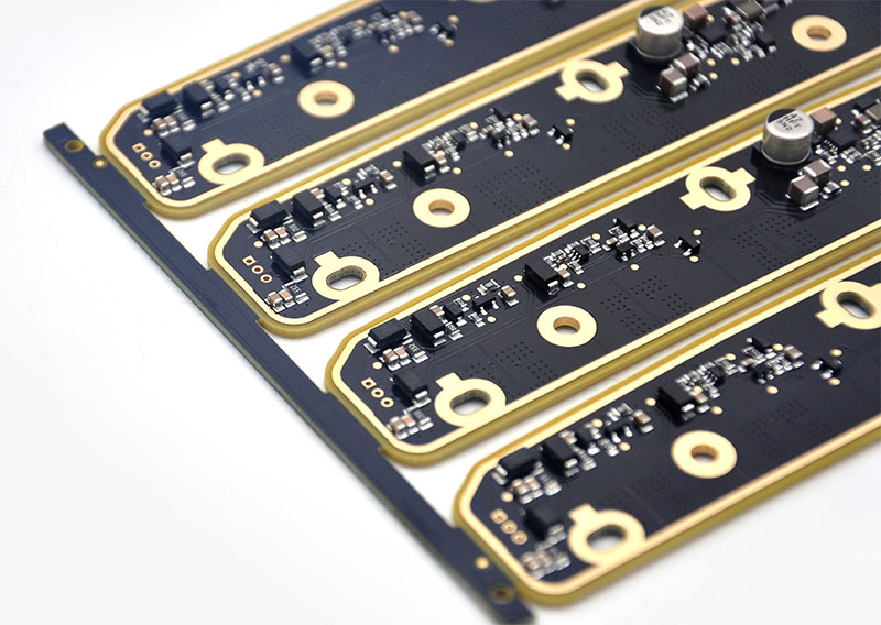
- PCB fabrication: Producing the bare board to your specification — layer count, copper weight, surface finish, and impedance requirements.
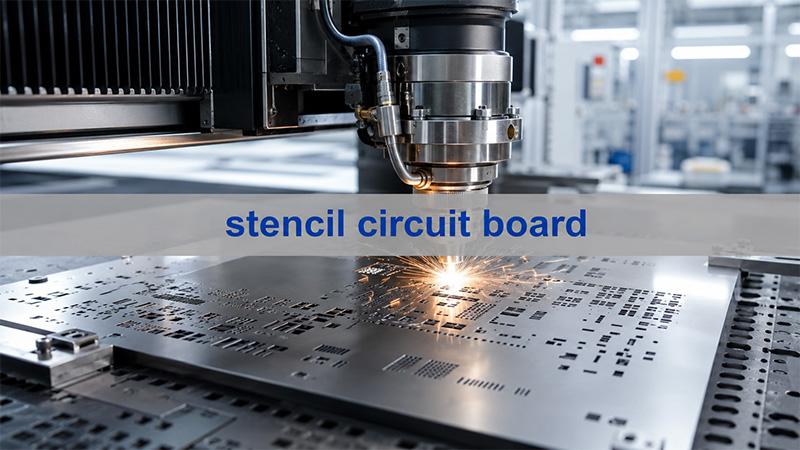
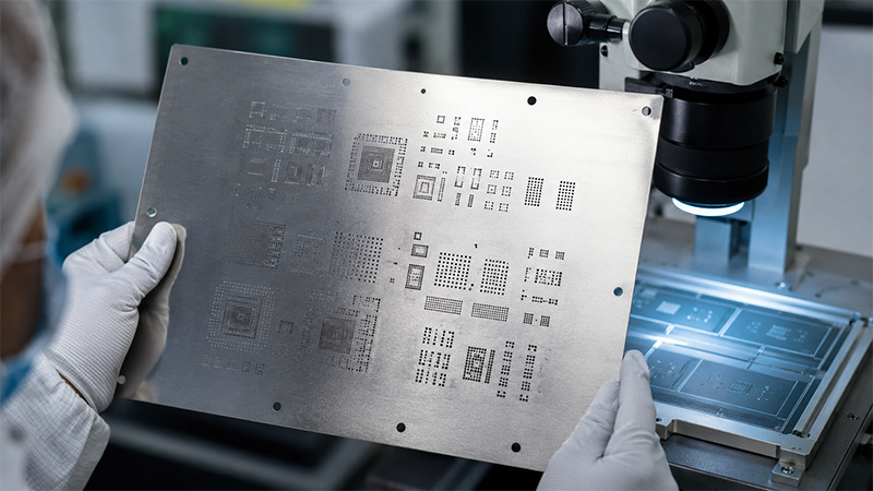
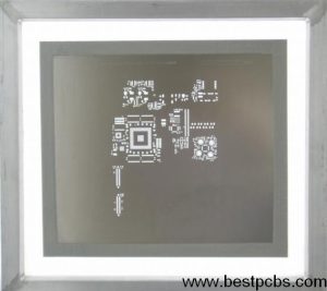
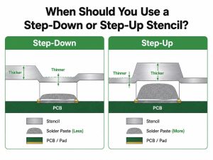
- Solder paste printing: Applying solder paste through a laser-cut stencil to all SMT pads with precise volume control.
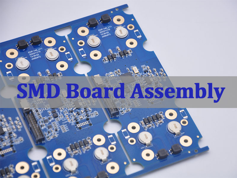
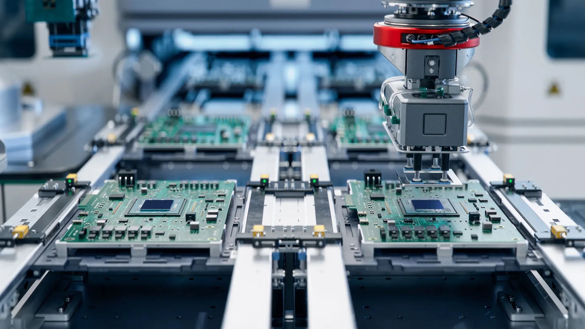
- SMT component placement: Automated pick-and-place running at up to 13,200,000 chips/day, handling components down to 01005 and BGA pitch as fine as 0.25 mm. Board sizes from 0.2 × 0.2 inches up to 22 × 47.5 inches are supported. Components are accepted in reels, cut tape, tube, tray, or loose parts.
- Reflow soldering: Controlled thermal profiling to achieve correct solder joint formation without thermal damage to components.
- Through-hole PCB assembly: Manual or wave soldering for connectors, transformers, electrolytic capacitors, and other leaded components.
- Automated Optical Inspection (AOI): Post-reflow inspection for solder bridges, missing components, polarity errors, and misalignment.
- X-ray inspection: For BGA and QFN components where solder joints are not visible from above.
- Functional and electrical testing: Verifying that the assembled board performs to specification under real operating conditions.
- Traceability documentation: Certificate of Conformance, test records, and component lot data shipped with every order.
Not every PCB assembly service provider offers all of these steps in-house. When critical steps are outsourced — particularly bare board fabrication or component procurement — quality control gaps appear at the handoff points. This is one of the strongest arguments for choosing a one-stop provider with owned facilities.
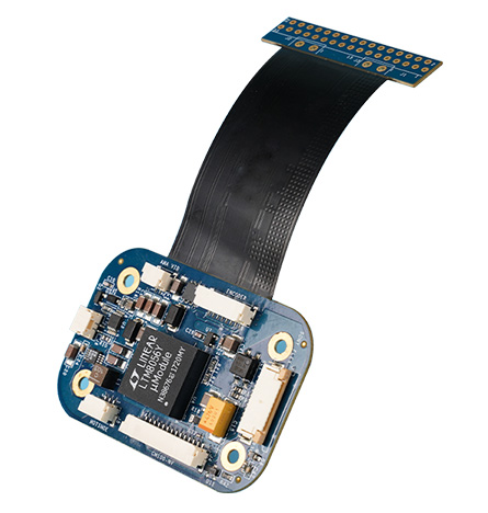
SMT Assembly Capabilities: Key Specifications
For engineers evaluating whether a PCB assembly service can handle their specific design, the table below summarizes our SMT line capabilities. These parameters apply to all order volumes from prototype to production.
| Item | Capability |
|---|---|
| Placer Speed | 13,200,000 chips/day |
| Bare Board Size | 0.2 × 0.2 inches minimum — 20 × 20 inches / 22 × 47.5 inches maximum |
| Minimum SMD Component | 01005 |
| Minimum BGA Pitch | 0.25 mm |
| Maximum Component Size | 50 × 150 mm |
| Assembly Type | SMT, THT, Mixed assembly |
| Component Package | Reels, Cut Tape, Tube, Tray, Loose Parts |
| SMT Process Lead Time | 1–5 days (SMT stage only) |
A few points worth noting for design engineers:
- 01005 capability means we can assemble the smallest passive components in mainstream production use today. If your design uses 0201 or larger, placement is well within standard process parameters.
- 0.25 mm BGA pitch covers the majority of high-density IC packages including memory devices, FPGAs, and application processors. If your BGA pitch is tighter than 0.25 mm, contact our engineering team before submitting files.
- Mixed assembly (SMT + THT) is handled as a single integrated workflow — not two separate jobs passed between departments. This matters for scheduling accuracy and accountability.
- Loose parts acceptance is particularly useful for prototype and small batch orders where full reels are not available or economical.
How to Prepare Your Files for PCB Assembly Services?
The quality of your output is directly proportional to the quality of your input files. Poorly prepared documentation is the single most common source of production delays and first-article failures. Before submitting to any PCB assembly service, your package should contain:
Gerber Files (RS-274X format)
Include all copper layers, solder mask layers top and bottom, silkscreen layers top and bottom, board outline, and drill files in Excellon format. Confirm that your CAD software has exported the correct layer polarity — solder mask layers should be negative, where open areas represent exposed copper.
Bill of Materials (BOM)
Your BOM must include manufacturer part number (MPN), manufacturer name, component value, package and footprint, reference designator, and quantity per board. Avoid listing only internal part numbers or generic descriptions. A BOM that says “100nF cap” without an MPN forces your assembly partner to make substitution decisions that may not match your design intent.
Assembly Drawings
Top and bottom assembly drawings showing component placement, polarity indicators for polarized components such as diodes, electrolytic capacitors, and ICs, and any special assembly notes — DNP components, conformal coating areas, or torque specifications for mechanical fasteners.
Pick-and-Place File
A centroid file exported from your CAD tool listing the X/Y coordinates, rotation, and board side for every SMT component. This file programs the pick-and-place machine and should be verified against your assembly drawing before submission.
Test Specification
If you require functional testing beyond standard electrical continuity, provide a written test procedure specifying test points, input conditions, expected output ranges, and pass/fail criteria.
A complete, well-documented package reduces DFM review time, eliminates back-and-forth clarification, and gets your boards into production faster.
DFM Review: What Gets Caught Before Production
Design for Manufacturability review is the most cost-effective quality intervention available. A defect caught at the DFM stage costs minutes to fix. The same defect found after assembly costs the full value of the build — plus rework labor, component replacement, and schedule delay.
Our engineering team reviews every incoming project against the following checklist before approving production:
- Land pattern vs. component body verification: Confirm that the PCB footprint matches the actual component package in your BOM. A 0402 footprint under a 0603 component causes tombstoning during reflow.
- Solder mask opening ratio: Verify that solder mask openings are correctly sized relative to pad dimensions. Openings that are too small cause insufficient solder; openings that are too large increase bridging risk on fine-pitch components.
- Courtyard clearance: Confirm minimum spacing between component courtyard boundaries to ensure pick-and-place nozzle access.
- Thermal relief on power pads: Check that power plane connections use appropriate thermal relief to allow even heat flow during soldering. Solid connections to large copper pours cause cold joints.
- Via-in-pad specification: Identify any vias within SMT pads and confirm whether they are specified as filled and capped. Unfilled via-in-pad causes solder wicking and voiding under QFN and BGA components.
- BOM completeness and cross-reference: Every reference designator in the Gerber must appear in the BOM with a valid MPN. Missing or mismatched entries are flagged before procurement begins.
- Component availability check: Flag any parts that are end-of-life, allocated, or single-source with lead times exceeding your delivery window. Alternative parts from our supply chain network are suggested where applicable.
- High-voltage clearance and creepage: For boards operating above 50 V, copper clearance and creepage distances are verified against IPC-2221 requirements.
- Polarity and orientation markers: Confirm that diodes, electrolytic capacitors, ICs, and connectors have correct polarity indicators in both silkscreen and assembly drawing.
- Impedance stack-up verification: For controlled impedance designs, model the stack-up against the Dk of the selected laminate and confirm that specified trace widths achieve the target impedance within tolerance.
Every project receives a written DFM Pre-Screening Report with findings categorized as Critical, Major, or Advisory — issued before production is approved, included at no additional charge.
Prototype PCB Assembly Services: What Engineers Need to Know
Prototype PCB assembly services serve a fundamentally different purpose than volume production. The goal is not throughput — it is learning. A prototype build exists to validate the schematic, confirm the layout, verify component choices, and surface any issues before committing to a larger run. Understanding what distinguishes good prototype assembly services from generic low-cost options helps engineers make better sourcing decisions early in the development cycle.
First-article inspection is essential for prototypes. Before the remainder of a prototype batch is assembled, a first-article inspection verifies the first completed unit against all design and BOM requirements. This provides a critical quality gate that is standard in our prototype process.
Stencil selection matters at low volume. For builds of 1–10 pieces, framed stencils are unnecessarily expensive. Frameless prototype stencils offer a cost-effective alternative with acceptable print quality for engineering validation. Our team recommends the appropriate stencil type based on your order volume and component density.
Iteration support is part of the service. Prototype orders often exist within an active design iteration cycle. Engineers need to modify BOMs between builds, change a footprint, or swap a component to resolve a performance issue. A PCB assembly service partner who accommodates mid-project changes without excessive administrative friction is genuinely valuable during development.
Component sourcing at small quantities requires a broad network. Buying components below distributor minimum order quantities — in cut-tape or single-reel quantities — requires a supplier network that can source small quantities without a significant price premium. Our 1,000+ supply chain partners provide access to small-quantity pricing that most engineers and small companies cannot negotiate independently.
Our minimum order quantity for prototype PCB assembly services is 1 piece. Standard lead time is 1.5 weeks from confirmed files and purchase order.
Quick Turn PCB Assembly Services: Speed Without Sacrificing Quality
Quick turn PCB assembly services are defined not just by speed but by the ability to maintain quality discipline under compressed timelines. The most common mistakes in quick turn work — skipping DFM review, accepting incomplete BOMs, using substitute components without engineering approval — are precisely the shortcuts that create expensive failures in the field.
Our quick turn PCB assembly services deliver full PCBA in 1.5 weeks (10–12 business days) as a standard offering, covering DFM review, component procurement, bare board fabrication, SMT assembly, AOI, and functional testing. For the most time-critical prototype requirements, express options are available.
What makes quick turn delivery realistic without cutting corners:
- In-house PCB fabrication: No waiting for a third-party board shop. Our own facility produces bare boards in parallel with component procurement, compressing the overall schedule.
- Stocked component inventory: For common passives, standard logic, and frequently specified active components, our warehouse carries inventory that eliminates procurement lead time on a significant portion of most BOMs.
- 24-hour DFM review: For standard complexity designs, our engineering team issues a written DFM report within 24 hours of receiving complete files — so production is not delayed by an extended review cycle.
- Fast SMT throughput: With a placer speed of 13,200,000 chips/day, SMT processing for most prototype and small batch builds is completed within 1–5 days, keeping the overall timeline tight.
- Digital workflow: Our manufacturing management system tracks every job in real time, flagging bottlenecks before they affect delivery. Material and batch traceability is available within 5 seconds for any unit.
Quick turn PCB assembly services are particularly valuable for: design validation builds ahead of a product review milestone, bug-fix iterations where a previous prototype revealed an issue, samples for customer evaluation or regulatory submission, and production bridge orders while long-lead-time components are inbound.
Low Volume PCB Assembly Services for Production
Low volume PCB assembly services — typically covering orders from 10 to 500 pieces — occupy a critical position in the product lifecycle. They are too large to treat as prototypes but too small to benefit from high-volume production economics. The challenges are specific and engineers who understand them make better sourcing decisions.
Setup cost amortization at low volume. Every PCBA job incurs fixed setup costs: stencil fabrication, pick-and-place programming, reflow profile development, and test fixture setup. At high volume, these costs spread across thousands of units. At low volume, they represent a higher proportion of per-unit cost. A PCB assembly service experienced in low volume work prices this honestly rather than quoting artificially low unit prices and recovering margin elsewhere.
Component procurement for small quantities. Low volume orders frequently require component quantities below standard reel minimums. Our supply chain network provides access to cut-tape and partial-reel sourcing across 1,000+ partners, enabling competitive component pricing for orders that larger contract manufacturers are not set up to handle efficiently.
PCB assembly services for low volume production benefit most from partners who can offer:
- Formal first-article inspection before the full batch is built
- Written DFM review with BOM optimization recommendations
- Flexible scheduling that accommodates design changes between builds
- Full traceability documentation matching production-level standards
- Pricing structures that scale predictably as volume grows
Our low volume PCB assembly services support orders from 10 pieces to 500 pieces with the same quality system, certification coverage, and traceability standards applied to higher-volume production.
Turnkey vs. Consignment PCB Assembly Services
Engineers choosing a PCB assembly service need to understand the difference between turnkey and consignment models — and which suits their project.
Turnkey PCB assembly services means the assembly provider sources all components, procures the bare boards, and delivers fully assembled units. The engineer supplies design files; the provider handles everything else. This model reduces engineering time spent on procurement, eliminates component quality risk from multiple supplier relationships, and simplifies project management. It is the right choice for most prototype and production builds, particularly when working with a provider who has a strong supply chain network.
Consignment PCB assembly services means the engineer supplies pre-purchased components, and the assembly provider handles only the assembly work. This model gives engineers direct control over component sourcing — useful when preferred suppliers are already qualified, when specific lot traceability is required for regulatory purposes, or when components have already been purchased. The tradeoff is that the engineer carries inventory risk and must coordinate component delivery to match the production schedule.
Partial consignment — a hybrid where the engineer supplies some components and the provider sources the remainder — is common in practice and is a standard option in our service model.
| Model | Engineer Supplies | Provider Supplies | Best For |
|---|---|---|---|
| Full Turnkey | Gerber files + BOM | All components + PCB + assembly | Most prototype and production builds |
| Consignment | All components + Gerber + BOM | Assembly only | Regulatory-controlled supply chains |
| Partial Consignment | Some components + files | Remaining components + PCB + assembly | Mixed sourcing requirements |
Through-Hole PCB Assembly Service: When It Applies
Through-hole PCB assembly service remains relevant for specific component types and applications despite the industry’s shift toward surface mount technology. Understanding when through-hole assembly is appropriate — and how it integrates with SMT in mixed-technology builds — helps engineers write more complete assembly specifications.
Through-hole assembly is applied for:
- High-current connectors that require the mechanical strength of through-board leads and solder joints in the barrel
- Electrolytic capacitors in power supply circuits where body size and lead pitch make through-hole the practical choice
- Power semiconductors mounted through the board for heat sink attachment on the opposite side
- Transformers and inductors with lead configurations designed for through-hole mounting
- Edge connectors and headers requiring the pull-out strength that through-hole solder joints provide
- Components in high-vibration environments where through-hole solder joints offer superior mechanical retention compared to SMT
In mixed-technology assemblies combining SMT and through-hole components, our process sequences SMT placement and reflow first, followed by through-hole insertion and wave or selective soldering. For boards where wave soldering would damage SMT components on the bottom side, selective soldering provides precise localized heating without thermal exposure to adjacent assemblies.
Our through-hole PCB assembly service is included as a standard capability at all order volumes from prototype to production.
Material and Surface Finish Selection
The bare board specification directly affects assembly yield, solder joint reliability, and long-term field performance. Here is a summary of the most relevant choices:
Laminate Selection
| Material | Tg Range | Best Application |
|---|---|---|
| FR4 Standard Tg | 130–140 °C | Consumer electronics, low-ambient industrial |
| FR4 Mid Tg | 150 °C | Industrial controls, higher operating temperature |
| FR4 High Tg | 170–180 °C | Automotive, high-power, lead-free assembly |
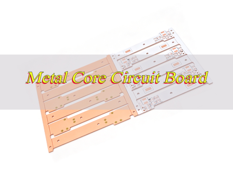
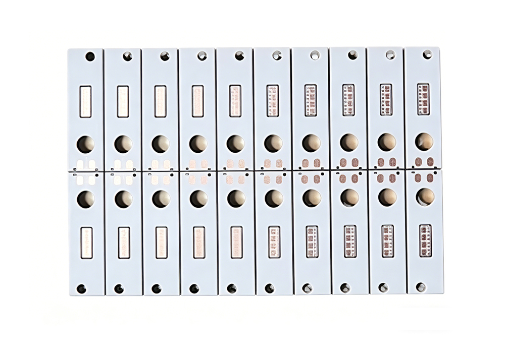
| Metal Core (Aluminum) | — | LED drivers, high-current power boards |
| High-Speed / Low-Loss | Low Dk/Df | GaN converters, high-frequency designs |
For lead-free assembly processes — which reach peak reflow temperatures of 245–260 °C — Mid Tg or High Tg laminates are strongly recommended to prevent laminate delamination during soldering.
Surface Finish Selection
| Surface Finish | Thickness | Key Advantage | Recommended For |
|---|---|---|---|
| Lead-Free HASL | 2–40 µm | Low cost, robust solderability | General industrial, cost-sensitive projects |
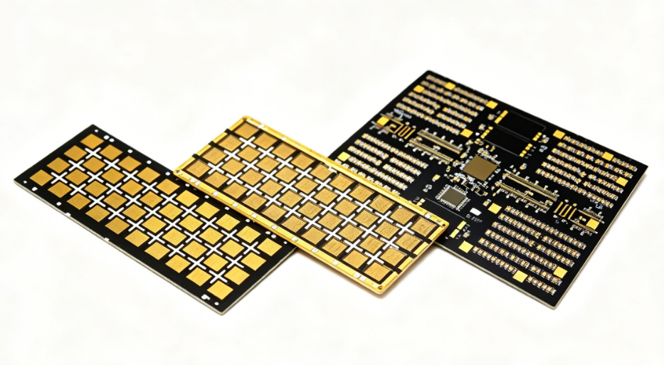
| ENIG | Ni: 3–8 µm / Au: 0.025–0.125 µm | Flat surface, long shelf life | Fine-pitch SMT, BGA, multi-reflow assemblies |
| Immersion Tin | 0.8–1.5 µm | Press-fit compatible, RoHS | Automotive with press-fit connectors |
| Immersion Silver | 0.2–0.4 µm | Excellent coplanarity | High-frequency boards |
| OSP | 0.1–0.3 µm | Flattest surface, lowest cost | Single-reflow, short storage window |
| ENEPIG | Ni/Pd/Au stack | Wire-bond and solder compatible | Hybrid modules, medical devices |
Certifications: What They Mean for Your Supply Chain
- ISO 9001:2015: The baseline quality management system standard. Covers process control, document management, and corrective action. A necessary condition for most regulated applications.
- ISO 13485:2016: Required for medical device supply chains. Covers traceability, risk management documentation, and sterile process controls. If your PCBA goes into a Class I, II, or III medical device, your assembly partner needs this certification.
- IATF 16949:2016: The automotive quality management standard for Tier 1 and Tier 2 suppliers. Covers PPAP, FMEA, control plans, and measurement system analysis. Required if your board goes into a vehicle.
- AS9100D: The aerospace and defense quality management standard. Covers configuration management, first-article inspection, and counterfeit parts prevention.
- IPC-A-610: The workmanship standard for PCB assembly. Class 2 applies to most industrial and consumer products; Class 3 applies to high-reliability applications including medical and military.
EBest Circuit holds ISO 9001, ISO 13485, IATF 16949, and AS9100D certifications — covering commercial industrial through automotive, medical, and aerospace applications.
Why Engineers Choose EBest Circuit for PCB Assembly Services?
20 years of focused PCBA experience. We have supported more than 10,000 engineers and 1,800+ customers across medical, automotive, industrial, aerospace, and consumer electronics sectors. This depth of experience is reflected in the engineering judgment our team brings to DFM review, process selection, and problem-solving during production.
One business partner, three-engineer technical team. Every project is assigned a dedicated team: one business partner managing communication and timelines, and three specialized engineers covering R&D, PCB process, and PCBA assembly. Technical questions are answered by the engineer responsible for that specific part of your build — not filtered through a generalist account manager.
Owned factory, no sub-contracting on critical processes. We own and operate our PCB fabrication facility and PCBA assembly line. Bare board production, component procurement, SMT assembly, inspection, and testing are all performed under our direct quality control.
1,000+ supply chain partners. Our supplier network covers broad BOM scope, small-quantity pricing for prototype orders, and alternative sourcing options when primary parts are allocated or end-of-life. Active counterfeit screening is performed for aerospace and medical builds.
5-second digital traceability. Our manufacturing system tracks material lots, production batches, and individual board serial numbers in real time. Complete manufacturing history for any unit in the field can be retrieved in under 5 seconds — essential for automotive PPAP and medical device traceability requirements.
Standard 1.5-week PCBA lead time. From confirmed Gerber files, BOM, and purchase order to shipped assembled boards: 10–12 business days. Express options available for urgent prototype requirements.
If you are evaluating PCB assembly service providers for a current or upcoming project, the fastest path to accurate pricing and a technical assessment is to send your Gerber files, BOM, and project requirements to sales@bestpcbs.com. Our engineering team reviews every inquiry personally and responds within 24 hours — whether your project is a 5-piece prototype or a 5,000-piece production run.
Visit www.bestpcbs.com for full capability specifications, certifications, and process documentation.
Frequently Asked Questions About PCB Assembly Services
What files do I need to submit to start a PCB assembly service order?
The minimum required file set is: Gerber files in RS-274X format, a complete Bill of Materials with manufacturer part numbers, an assembly drawing showing component placement and polarity, and a pick-and-place centroid file. If functional testing is required beyond electrical continuity, a written test specification is also needed. Our engineering team reviews every submission within 24 hours and flags any missing items before production begins.
What is the minimum order quantity for PCB assembly services?
Our minimum order quantity is 1 piece. We assemble single-unit engineering prototypes as well as production runs of tens of thousands of units. Prototype and small batch orders carry higher per-unit costs due to setup amortization, while orders above 500 pieces benefit from significantly lower unit pricing.
How quickly can you turn around a prototype PCB assembly order?
Our standard lead time for full PCBA — covering DFM review, component procurement, bare board fabrication, SMT assembly, AOI, and testing — is 1.5 weeks (10–12 business days) from confirmed files and purchase order. The SMT stage alone is completed within 1–5 days. For engineering prototypes where components are in stock, overall lead times can be shorter. Express service is available for urgent requirements.
Do you offer quick turn PCB assembly services?
Yes. Our 1.5-week standard lead time already represents a quick turn capability relative to industry averages for full turnkey PCBA. For even faster turnaround on prototype builds with stocked components and complete files, please contact our engineering team at sales@bestpcbs.com to discuss express options.
Can you assemble boards with both SMT and through-hole components?
Yes. Mixed-technology assemblies combining SMT and through-hole components are a standard capability. Our SMT line handles components down to 01005 with BGA pitch as fine as 0.25 mm. Through-hole components are processed by wave soldering, selective soldering, or manual hand soldering depending on the board layout. Press-fit connector installation is also available.
What is the difference between turnkey and consignment PCB assembly services?
Turnkey means the assembly provider sources all components and produces the bare boards — the engineer supplies design files only. Consignment means the engineer supplies pre-purchased components and the provider handles assembly. Partial consignment, where the engineer supplies specific components and the provider sources the remainder, is also a standard option. Most prototype and low volume production builds benefit from the turnkey model due to reduced procurement overhead.
Do you provide PCB assembly services for low volume production?
Yes. We regularly support low volume production orders from 10 to 500 pieces with the same quality system, certification coverage, DFM review, and traceability standards as higher-volume builds. Low volume PCB assembly services are priced to reflect actual setup costs transparently, without hidden fees.
Which certifications does EBest Circuit hold?
We hold ISO 9001:2015, ISO 13485:2016 for medical devices, IATF 16949:2016 for automotive, and AS9100D for aerospace and defense. All certifications are maintained through regular third-party audits. Copies of current certificates are available on request.