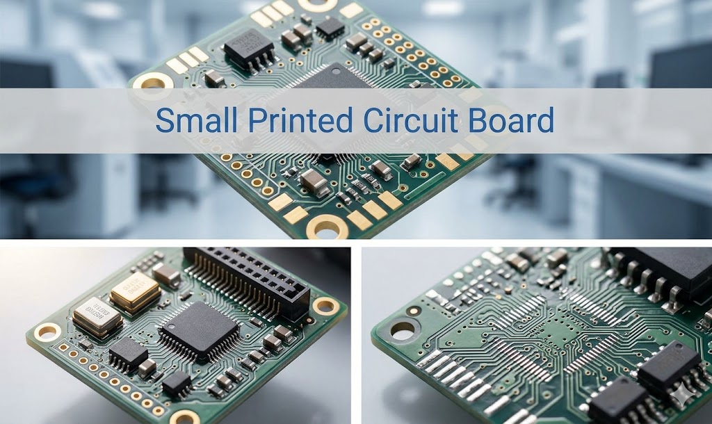
A small printed circuit board serves as the miniature backbone for compact electronic devices, enabling high-density interconnections in limited spaces. This article explores the technical nuances, manufacturing standards, and cost factors associated with producing these intricate assemblies.
Are you struggling with the unique challenges that come with miniaturized electronics?
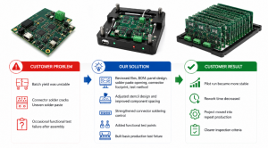
- My design has tiny components, but I keep getting poor yields due to soldering defects.
- We only need 5 or 10 pieces for the prototype, yet every supplier demands a massive MOQ.
- It is frustrating when signal interference ruins my RF performance in a dense layout.
- I cannot find a factory that understands the precision needed for micro-vias and fine traces.
- Getting a clear and accurate price for a small batch is nearly impossible with all the hidden fees.
As a professional PCBA manufacturer, we address these challenges directly:
- We deploy precision SMT placement machines to handle miniature components reliably.
- Our flexible production lines support printed circuit board small quantity runs with no MOQ.
- We design and integrate custom printed circuit board small rf shielded enclosures.
- Our 20-year engineering team specializes in small printed circuit board fabrication.
- We provide transparent quotations and a detailed small printed circuit board pricelist upfront.
With two decades of experience, EBest Circuit (Best Technology) has become a trusted partner for engineers worldwide. Our strengths lie in combining deep technical expertise with responsive manufacturing capabilities. We offer a true one-stop service covering PCB fabrication, component sourcing, assembly, and functional testing. Backed by ISO 9001, IATF 16949, ISO 13485 and AS9100D certifications, we ensure quality compliance across industries. Our in-house facilities, coupled with a supply chain of over 1,000 partners, allow us to manage everything from prototypes to small-batch production efficiently. This infrastructure supports rapid R&D iteration while maintaining full traceability through our digital workshop system. For inquiries, pls feel free to contact us at sales@bestpcbs.com.
What is Small Printed Circuit Board?
A small printed circuit board typically refers to two distinct but interlinked concepts in the electronics industry: miniaturized physical dimensions and low-volume production runs.
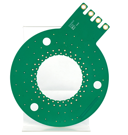
Physically, it is a high-density interconnect (HDI) board engineered to fit into compact devices like wearables, medical sensors, and IoT modules. These boards demand extreme precision, often featuring line widths and spaces as fine as 2mil (0.05mm) and laser-drilled micro-vias of 0.1mm. Because of their tiny footprint, they require specialized fabrication techniques to ensure signal integrity and thermal stability.
From a manufacturing perspective, “small” also pertains to small-batch or prototype assembly. This service is vital for engineers who need a limited quantity (often 5 to 100 units) to validate a design before scaling to mass production. At EBest Circuit (Best Technology), we bridge the gap between these two definitions by providing high-precision, small-sized boards with No MOQ requirements, supporting your project from the first micro-prototype to full-scale market deployment.
What are the small holes in printed circuit boards called? (Vias & Through-holes)
Understanding the terminology and function of plated holes is fundamental when designing a small printed circuit board. These features are not merely drilled openings; they are conductive pathways that determine the electrical integrity and layer transitions of your circuit. Properly specifying these elements ensures signal continuity and mechanical stability in high-density designs.
| Type | Function | Specs / Notes |
|---|---|---|
| Through-Hole | Top-to-bottom layer connection | For THT parts; min. drill Ø ~0.2mm. |
| Micro-via | Adjacent layer connection (HDI) | Laser-drilled; often copper/resin-filled. |
| Blind Via | Outer to inner layer connection | Non-through-hole; depth/diameter ratio critical. |
| Buried Via | Internal layer connection only | Hidden within board; requires extra lamination. |
| Thermal Via | Heat transfer from components | Under thermal pads (e.g., QFN); aids cooling. |
- Aspect Ratio: Maintain an aspect ratio (board thickness / hole diameter) of 8:1 or less for reliable plating.
- Annular Ring: Ensure the copper pad surrounding the hole is at least 0.05mm to prevent breakout during drilling.
- Via-in-Pad: Requires plugging and capping to prevent solder wicking; common in small printed circuit board layouts.
- Tenting Vias: Covering vias with solder mask to prevent solder paste from entering the hole during reflow.
Selecting the correct via structure is essential for optimizing space and performance in your small printed circuit board. By aligning your design choices with fabrication capabilities, you minimize the risk of open circuits and manufacturing delays.
Key Components and Design: Small Printed Circuit Board Capacitors and Layout
Component selection and placement are critical in constrained layouts, especially regarding small printed circuit board capacitors. These passive components influence everything from power integrity to signal timing, requiring careful consideration during schematic design and layout phases. A well-executed plan prevents noise coupling and ensures stable operation.
- Capacitor Types: Choose NP0/C0G for high-frequency stability and X7R/X5R for bulk decoupling based on dielectric needs.
- Package Size: Common compact packages include 0201 (0.6mm x 0.3mm) and 0402 (1.0mm x 0.5mm) for dense placement.
- Placement Rules: Place decoupling capacitors as close as possible to the power pins of ICs to minimize loop inductance.
- Thermal Relief: Use appropriate pad geometry to avoid tombstoning during reflow soldering of small parts.
- Land Pattern: Follow IPC-7351 standards for footprint creation to ensure compatibility with automated assembly.
- BOM Optimization: Our engineering team reviews your bill of materials to suggest second-source components for better availability.
| Parameter | Typical Value / Guideline | Impact on Design |
|---|---|---|
| ESR (Equivalent Series Resistance) | < 20 mΩ for low-noise applications | Affects power supply ripple and transient response. |
| Voltage Rating | At least 150% of operating voltage | Prevents capacitor failure under surge conditions. |
| Pad-to-Pad Clearance | ≥ 0.1mm for 0201 components | Ensures solder bridging does not occur during assembly. |
Working with experienced assemblers helps navigate the trade-offs between component size, cost, and reliability. Proper layout techniques guarantee that even the smallest capacitors perform their intended function without compromising the overall board integrity.
Solving Interference: Printed Circuit Board Small RF Shielded Enclosures
Radio Frequency (RF) designs are particularly susceptible to Electromagnetic Interference (EMI), making shielding a necessity for sensitive circuits. Incorporating printed circuit board small rf shielded enclosures protects vulnerable components from external noise and contains emissions within regulatory limits. This approach is vital for wireless modules operating in the MHz to GHz range.
- Shielding Can Types: Use stamped metal cans (e.g., nickel-plated copper) soldered directly to the PCB ground plane.
- Material Selection: Choose materials like cold-rolled steel or brass for optimal magnetic and electric field attenuation.
- Ventilation & Heat: Design enclosures with perforations or gaps sized significantly smaller than the wavelength of interest.
- Grounding Strategy: Ensure the shield connects to a low-impedance ground path to effectively sink induced currents.
- Coaxial Transitions: Route RF signals through the shield wall using filtered connectors or feedthrough capacitors.
| Frequency Range | Recommended Shield Material | Typical Attenuation |
|---|---|---|
| 100 MHz – 1 GHz | Nickel-Silver Alloy | 40 – 60 dB |
| 1 GHz – 10 GHz | Tin-Plated Steel | 60 – 80 dB |
| > 10 GHz | Solid Copper with Gaskets | > 90 dB |
Effective shielding requires a holistic view of the design, considering both mechanical and electrical interactions. By integrating enclosure design early, you prevent costly re-spins and ensure compliance with FCC or CE standards.
Industry Standards for Small Printed Circuit Board Fabrication and Factories
Adhering to recognized industry standards separates hobby-grade work from professional manufacturing. Reputable small printed circuit board factories operate under strict quality management systems to deliver consistent results. Understanding these benchmarks helps you vet potential suppliers and align expectations.
- IPC-A-600: Acceptability of Printed Boards—defines criteria for visual inspection of base PCBs.
- IPC-A-610: Acceptability of Electronic Assemblies—classifies solder joint quality (Class 2 vs. Class 3).
- ISO 9001: Quality Management Systems ensuring process control and continuous improvement.
- IATF 16949: Automotive-specific standard requiring APQP, PPAP, and FMEA documentation.
- AS9100D: Aerospace standard emphasizing safety, reliability, and configuration management.
| Certification | Primary Focus | Benefit for Customer |
|---|---|---|
| ISO 13485 | Medical Devices | Ensures traceability and biocompatibility controls. |
| UL Certification | Safety Compliance | Recognized safety mark for North American markets. |
| RoHS / REACH | Environmental Compliance | Guarantees restriction of hazardous substances. |
Partnering with a factory that holds these certifications provides assurance that your product will meet the rigorous demands of its target application. It reflects a commitment to process discipline and risk mitigation.
Why Opt for Printed Circuit Board Small Quantity Assembly Services?
Engineers frequently face the dilemma of needing professional assembly for limited runs without committing to mass production volumes. Printed circuit board small quantity assembly services bridge this gap, offering the precision of high-volume lines with the flexibility required for R&D. This model accelerates development cycles and reduces time-to-market.
- Rapid Prototyping: Quickly validate design concepts before investing in expensive tooling.
- Lower Financial Risk: Avoid tying up capital in large inventory batches that may become obsolete.
- Design Iteration: Easily incorporate changes between builds based on test feedback.
- Access to Technology: Utilize advanced processes like laser drilling and X-ray inspection on small lots.
- Simplified Logistics: Manage a single purchase order instead of separate contracts for PCB and assembly.
This approach empowers engineering teams to fail fast, learn quickly, and refine their products efficiently. It is an indispensable strategy for startups and established companies alike.
Finding the Right Partner: Small Batch Printed Circuit Board Assembler Benefits
Selecting a competent small batch printed circuit board assembler goes beyond comparing price quotes; it involves evaluating technical support and responsiveness. The right partner acts as an extension of your engineering team, contributing insights that improve manufacturability and yield.
- DFM Analysis: Receives a free Design for Manufacturability report highlighting potential assembly issues.
- Supply Chain Access: Leverages established relationships with authorized distributors for genuine components.
- Flexible Scheduling: Accommodates urgent changes and rush orders without derailing production flow.
- Technical Consultation: Provides direct access to senior process engineers for troubleshooting assembly defects.
- Quality Documentation: Delivers full inspection reports, including AOI, X-ray, and flying probe data.
These benefits compound over the lifecycle of a project, resulting in higher quality products and smoother production ramp-ups. A collaborative relationship fosters innovation rather than simply executing instructions.
Production Flexibility: The Advantages of Small Run Printed Circuit Boards
The ability to order small run printed circuit boards provides unparalleled agility in today’s fast-paced electronics market. This flexibility allows companies to test multiple design variants simultaneously or produce limited edition products without excessive waste. It aligns manufacturing output precisely with demand.
- NPI Support: New Product Introduction flows smoothly from design to production with minimal lead time.
- Inventory Management: Just-in-Time (JIT) production reduces warehousing costs and minimizes excess stock.
- Customization: Enables niche or specialized versions of a product without retooling an entire line.
- Cost Efficiency: Spreads development costs over several small runs instead of one large, risky investment.
- Quick Turnaround: Many providers offer 24-hour or 48-hour build cycles for simple small run printed circuit boards.
Embracing this production model future-proofs your operations against fluctuating market demands. It transforms manufacturing from a rigid constraint into a strategic advantage.
While we excel in miniaturized designs—supporting ultra-fine line/space down to 2mil/2mil (0.05mm) and minimum laser drill sizes of 0.1mm—our capabilities are not limited to small batches. Once your prototype is validated, our fully automated production lines are equipped to scale up to high-volume mass production. We seamlessly transition your project from initial R&D to large-scale supply, maintaining the same rigorous IATF 16949 and ISO standards throughout the product lifecycle.
How much does it cost for small printed circuit board?
Determining how much does it cost for small printed circuit board projects depends on a matrix of variables rather than a fixed unit price. While simple two-layer boards might cost a few dollars, complex multi-layer assemblies can increase exponentially. Understanding these drivers helps you budget accurately and identify cost-saving opportunities.
- Layer Count: Each additional layer adds processing steps; a 4-layer board costs more than a 2-layer board.
- Material Type: Standard FR-4 is economical, whereas Rogers or polyimide materials command premium prices.
- Surface Finish: ENIG (Electroless Nickel Immersion Gold) costs more than HASL but offers superior planarity.
- Quantity: Economies of scale apply; the per-unit cost drops significantly as volume increases.
- Assembly Complexity: High component density and fine-pitch parts require more precise placement and inspection.
| Factor | Low-Cost Scenario | High-Cost Scenario |
|---|---|---|
| Layers | 2 Layers | 8+ Layers (HDI) |
| Board Size | 50mm x 50mm | 100mm x 100mm |
| Components | 20 SMD (all 0805+) | 150 Mixed (QFN, BGA) |
| Turnaround | 2 Weeks | 3 Days (Expedited) |
| Estimated Cost | 15–30 per unit | 120–250 per unit |
Always request a detailed breakdown rather than a lump-sum quote to understand where your money is going. This transparency allows for informed decisions about value engineering.
Understanding the Small Printed Circuit Board Pricelist and Cost Factors
A comprehensive small printed circuit board pricelist itemizes every charge, eliminating surprises later in the process. Scrutinizing this document reveals the manufacturer’s transparency and helps you compare bids objectively. Key line items typically include engineering fees, tooling charges, and recurring production costs.
- Tooling / Setup Fee: One-time charge for creating Gerber files, generating stencils, and programming pick-and-place machines.
- Raw Material Cost: Calculated based on panel utilization; larger panels reduce per-board cost.
- Labor Cost: Reflects the complexity of assembly; hand-soldering or manual rework increases expenses.
- Testing Fees: Includes ICT (In-Circuit Test), FCT (Functional Test), and boundary scan (JTAG/SWD) costs.
- Certification Premiums: Additional costs may apply for specialized audits or material certifications.
| Service Tier | Description | When to Use |
|---|---|---|
| Basic Build | PCB Fab Only | You handle assembly and sourcing separately. |
| Standard Turnkey | PCB + Assembly + Basic SMT | Ideal for most prototype and small batch needs. |
| Premium Service | Full Turnkey + Box Build + Cable Assembly | Complete system integration for end-product shipment. |
Reviewing these details ensures you receive fair value and helps establish a predictable cost structure for future projects.
A small printed circuit board is indispensable for modern electronics, balancing compactness with functionality across diverse applications. Throughout this article, we examined the technical definitions, design considerations, manufacturing standards, and financial aspects involved in producing these intricate assemblies. EBest Circuit (Best Technology) combines deep engineering insight with agile manufacturing to solve the specific pain points engineers face daily. From DFM analysis and BOM optimization to rapid small-batch assembly, we provide the tools and support necessary for successful product development. Just feel free to contact our team anytime at sales@bestpcbs.com.
FAQs About Small Printed Circuit Board
Q: What are the small holes in printed circuit boards called?
A: The small plated holes are generally called vias (vertical interconnect accesses) or through-holes. Micro-vias are tiny laser-drilled holes used in HDI designs, while through-holes pass completely through the board. Their primary function is to create electrical connections between different layers of the PCB.
Q: How much does it cost for a small printed circuit board prototype?
A: Prototype costs vary widely based on complexity, typically ranging from 15 to100 per board. Factors include layer count, material choice (e.g., FR-4 vs. Rogers), surface finish (ENIG vs. HASL), and component density. Ordering a small batch printed circuit board assembler service usually includes setup fees, so getting a detailed pricelist is essential.
Q: Can I get printed circuit board assembly for small quantity orders?
A: Yes, many manufacturers specialize in printed circuit board small quantity assembly. This service supports engineers who need 5 to 100 units for validation without paying for mass production tooling. Look for partners with digital workshops that allow quick changeovers and material traceability.
Q: What is the typical lead time for small run printed circuit boards?
A: Standard lead times for small run printed circuit boards are usually 1.5 to 3 weeks. However, expedited services can deliver in as little as 24 to 72 hours for simpler designs. Lead time depends heavily on material availability, layer count, and whether components need to be sourced.
Q: Are there specific factories for small printed circuit board fabrication?
A: Absolutely. Specialized small printed circuit board factories focus on high-mix, low-volume production. They invest in precision equipment like laser direct imaging (LDI) and high-resolution drills capable of handling fine traces and micro-vias required for compact designs.