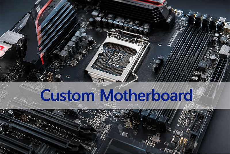
Custom Motherboard PCBs are the backbone of high-end electronics, serving as the central, custom-designed printed circuit board that integrates and connects all critical components within a system. This article will cover the entire journey of creating a custom motherboard, from initial layout design and rigorous verification to prototype fabrication, mass production requirements, and how to select the right manufacturing partner to ensure performance and reliability.
Are you grappling with the complex challenges of bringing a bespoke motherboard from concept to a reliable, high-performance product?
- Struggling with signal integrity issues like crosstalk and EMI in dense, multi-layer layouts, leading to unstable prototype performance.
- Facing costly delays and re-spins due to overlooked Design for Manufacturability (DFM) errors that only surface during PCBA assembly.
- Dealing with the headache of sourcing long-lead-time or obsolete components, which stalls your entire project timeline.
- Worrying about inconsistent quality and yield between your prototype run and the final mass production batch.
- Feeling lost without responsive technical support when urgent design tweaks or production issues arise mid-project.
As a professional PCBA manufacturer, EBest Circuit (Best Technology) addresses these challenges directly with tailored solutions:
- Our 20-year experienced engineering team provides in-depth DFM analysis and layout optimization advice specifically for complex, multi-layer motherboard designs to preempt signal and thermal issues.
- We deliver a comprehensive DFM pre-screening report and BOM optimization list before fabrication, catching potential assembly faults early to save time and cost.
- Our one-stop service integrates PCB fabrication with component sourcing from a network of 1,000+ vetted partners, ensuring authentic parts and streamlined supply chain management.
- We maintain consistent, certified processes from prototype to mass production, supported by in-house PCB and PCBA factories for end-to-end quality control.
- Our ‘1+3’ Support Model ensures elite project care, pairing you with one dedicated account manager and three specialist engineers for rapid, expert solutions from prototype to production.
EBest Circuit (Best Technology) is a professional PCB and PCBA manufacturer with over 20 years of expertise in serving the high-end electronics industry. Our strength lies in a full turnkey solution, where our seasoned engineering team provides DFM analysis and process adaptation from the start. We support everything from PCB design and fabrication—including advanced boards like heavy copper, HDI, and RF PCBs—to component sourcing, PCBA assembly, and full box build. Holding certifications like ISO 9001, IATF 16949, AS9100D, and ISO 13485, our in-house facilities and digital workshop enable precise batch traceability and rapid iteration for both prototypes and small-batch production. With a history of serving over 1,800 clients, we are committed to delivering comprehensive, high-quality solutions with a focus on on-time delivery. For inquiries, pls feel free to contact us at sales@bestpcbs.com.
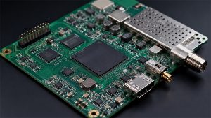
What Is a Custom Motherboard PCB in High-End Electronics?
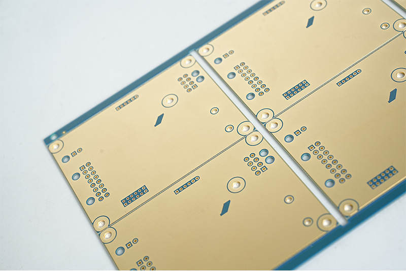
A custom motherboard PCB is the central, application-specific circuit board engineered to be the core of a dedicated electronic system, unlike standard off-the-shelf models. In high-end applications—from advanced gaming rigs and high-performance computing clusters to specialized industrial controllers and medical imaging systems—these boards are tailored to meet exact spatial, thermal, electrical, and functional requirements. This section explores the defining characteristics and critical role of a custom PC motherboard in pushing the boundaries of technology.
The value of a custom built motherboard lies in its optimized integration. Key specifications typically include:
- High Layer Count: Often 8 layers or more (capable up to 32 layers for FR4) to accommodate complex power and signal routing, reducing noise and crosstalk.
- Controlled Impedance: Critical for high-speed data buses (e.g., DDR memory, PCIe). Tolerances are tight, typically ±10% for values >50Ω and ±5Ω for values ≤50Ω.
- Advanced Materials: Use of High-Tg FR4 (e.g., Tg ≥170°C), low-loss laminates for RF sections, or even Metal Core PCBs (MCPCBs) for thermal management in power-intensive areas.
- Fine Features: Minimum trace/space can go down to 2.5/2.5 mil for inner layers and 3/3 mil for outer layers (with 1 oz copper), supporting high-density interconnects (HDI).
- Multiple Surface Finishes: Selection of ENIG, ENEPIG, or hard gold for edge connectors (gold fingers) based on durability and signal integrity needs.
- Rigorous Testing: 100% electrical testing (E-test) and flying probe testing for prototypes are mandatory to ensure connectivity and function before PCBA.
The custom motherboard is therefore not just a carrier of components but a precision-engineered substrate that determines the ultimate performance, reliability, and scalability of the entire system. Its design and fabrication set the foundation for all subsequent assembly and integration steps.
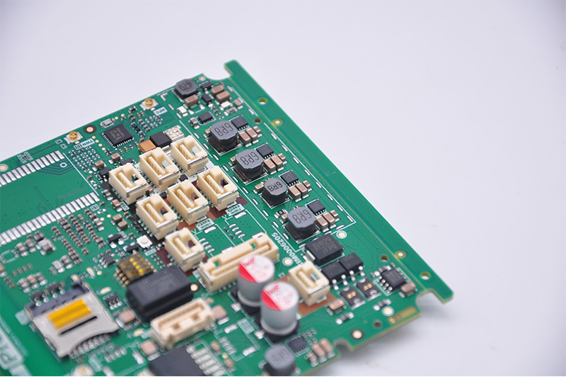
How Are Custom Motherboards Formed From PCB and PCBA?
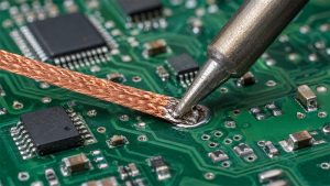
The formation of a functional custom motherboard is a two-stage symphony: first, the fabrication of the bare Printed Circuit Board (PCB), and second, the assembly of components onto it (PCBA). The PCB serves as the foundational platform with its intricate copper tracings, while the PCBA process populates this platform with ICs, connectors, and passive components, breathing life into the design. Understanding this seamless transition is key to planning a successful custom motherboard project.
The journey from a PCB panel to a ready-to-use custom built motherboard involves a detailed, interconnected workflow:
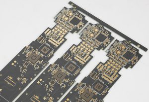
- PCB Fabrication: This starts with the manufactured bare board. For a complex motherboard, this involves multi-layer lamination, precision drilling of micro-vias (laser drill capability down to 0.1mm), and plating. Key outputs are the physical boards meeting all specified impedance, thickness, and finish requirements.
- Component Procurement & Kitting: Parallel to or after PCB fab, all components from the BOM are sourced. A reliable manufacturer uses authorized distributors to avoid counterfeits and can provide BOM optimization advice.
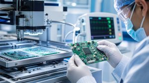
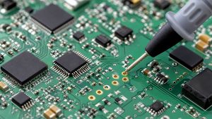
- SMT Assembly: Surface Mount Technology lines place microscopic components (down to 01005 size) using high-precision pick-and-place machines. A full nitrogen reflow oven ensures perfect solder joints for BGA packages with pitches as fine as 0.25mm.
- THT Assembly & Conformal Coating: Through-hole components (like large connectors or power sockets) are inserted, often via selective or wave soldering. Conformal coating may be applied for environmental protection.
- Inspection & Testing: This is critical. Automated Optical Inspection (AOI) and X-ray (for BGA joints) check for assembly defects. In-circuit Test (ICT) or Flying Probe Test verifies electrical performance. For motherboards, Functional Test (FCT) simulating real operation is often required.
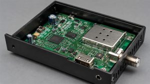
- Programming & Boxing: Firmware is loaded onto onboard memory. Finally, the assembled PCBA may be integrated into an enclosure or delivered as a complete system (box build).
This integrated PCB and PCBA flow underscores the need for a manufacturer that controls both processes. Any disconnect between the board fabrication tolerances and the assembly process windows can lead to failures, making a one-stop, turnkey service provider like EBest Circuit (Best Technology) a strategic advantage for custom motherboard realization.
How to Optimize Your Layout for a Custom Motherboard PCB?
Layout optimization is the strategic placement and routing of components and traces on a custom motherboard PCB to achieve optimal electrical performance, thermal management, manufacturability, and reliability. A poorly optimized layout can doom even the most well-conceived schematic, leading to signal integrity nightmares, overheating, and assembly failures. For a custom motherboard that often integrates high-speed processors, memory, and various I/Os, this phase is arguably the most critical in the design cycle.
Optimizing a custom motherboard layout requires balancing electrical and physical constraints. Here are key actionable strategies:
- Stack-up Planning: Define your layer stack-up early with your manufacturer. For an 8-layer board, a common stack like [Sig-Gnd-Pwr-Sig-Sig-Pwr-Gnd-Sig] provides good signal return paths. Use controlled dielectric materials (e.g., Dk ~4.2 for standard FR4, lower for high-speed sections) and aim for target impedance values (e.g., 50Ω for single-ended, 100Ω for differential pairs).
- Power Distribution Network (PDN): Use dedicated power and ground planes. For high-current rails (like CPU Vcore), calculate required copper weight (e.g., 2 oz or more) and use multiple vias for current sharing. Implement proper decoupling capacitor placement—use a mix of bulk, ceramic, and high-frequency caps close to power pins.
- High-Speed Signal Routing: Route critical signals (e.g., DDR, PCIe) with length matching (tolerance within ±5 mils for differential pairs) and maintain consistent impedance. Provide adequate spacing (3x trace width minimum) to minimize crosstalk. Avoid splitting reference planes beneath high-speed traces.
- Thermal Management: Identify hot components (CPUs, FPGAs, VRMs) and plan for thermal relief. Incorporate thermal vias under pads to conduct heat to inner copper layers or a metal core. In designs with localized high heat, consider specifying a Metal Core PCB (MCPCB) section with thermal conductivity of 1.5-3.0 W/m·K.
- DFM-Centric Design: Adhere to your manufacturer’s capabilities. For example, maintain a minimum solder mask bridge of 6-8 mil, a minimum annular ring of 8 mil for vias, and trace/space rules that match your chosen copper weight (e.g., 5/7 mil for 2 oz outer layer). Avoid acute angles in traces.
By methodically applying these principles, you transform a schematic into a manufacturable, high-performance board layout. Partnering with a manufacturer that offers custom motherboard design review services can provide invaluable feedback at this stage, catching potential issues before they are etched in copper, saving significant time and cost.
Why Is Custom Motherboard Design Verification Critical for PCBA?
Custom motherboard design verification is a rigorous, multi-faceted checking process that occurs after layout completion but before committing to fabrication. It is critical for PCBA because it identifies and rectifies design flaws that are far cheaper to fix in software than on physical boards. A single uncaught error—a missed connection, an incorrect footprint, or a violated design rule—can lead to non-functional assemblies, costly rework, and project delays, undermining the entire custom motherboard project.
A comprehensive verification strategy for a custom PC motherboard should include the following checks:
- Electrical Rule Check (ERC): Validates logical connectivity against the schematic, ensuring all nets are properly driven and terminated, and checking for floating pins or shorted outputs.
- Design Rule Check (DRC): Enforces physical layout constraints provided by the manufacturer. This includes checks for minimum trace width/space (e.g., 4/4 mil for normal FR4), drill-to-copper clearance (≥0.18mm for through-holes), and solder mask slivers.
- Signal Integrity (SI) & Power Integrity (PI) Simulation: Uses field solvers to analyze signal quality (overshoot, crosstalk, timing) on high-speed nets and to model the impedance of the Power Distribution Network, identifying voltage drop and resonance issues before building the board.
- Thermal Simulation: Models the board’s thermal performance under load, identifying hotspots that may require additional cooling measures like heatsinks, thermal vias, or a different substrate material (e.g., switching to an Aluminum PCB section).
- Design for Manufacturability (DFM) Analysis: A manufacturer-led review using their specific process capabilities. They check for issues like acid traps, copper slivers, inadequate annular rings, and impractical aspect ratios for plating (e.g., a maximum 8:1 aspect ratio for through-holes).
- Design for Assembly (DFA) Analysis: Focuses on the PCBA phase. Checks include component spacing for soldering tool access, polarity markings, stencil aperture design for proper paste volume, and suitability of selected surface finish (e.g., ENIG for fine-pitch BGAs).
Skipping or shortening these verification steps is a high-risk gamble. A single PCBA run for a complex custom motherboard represents a significant investment in boards and components. Thorough verification, especially a professional DFM/DFA report from your manufacturing partner, is the most effective insurance policy to ensure your first prototype assembly has the highest chance of success, accelerating your path to a validated, production-ready design.
How Do We Fabricate Prototypes for Complex Custom Motherboards?
Fabricating prototypes for complex custom motherboards is a specialized service that bridges the gap between design and validation, allowing engineers to physically test and iterate their concepts. It involves manufacturing small quantities of the fully assembled board with the same care and access to advanced processes as mass production. For a custom motherboard, where cost and complexity are high, a reliable and fast prototype service is indispensable for de-risking the project before committing to volume orders.
The prototype fabrication process at a full-service manufacturer like EBest Circuit integrates several key stages:
- Rapid PCB Prototyping: The bare PCB is fabricated first. For standard FR4 motherboards, fastest service can be as quick as 24 hours for 1-2 layer boards and 48-72 hours for 4-8 layer boards. Advanced features like HDI (laser drilled 0.1mm microvias) and heavy copper (up to 20 oz) are available even for prototype quantities.
- Expedited Component Sourcing: The manufacturer procures all components, often leveraging existing distributor relationships and in-house inventory for common parts to avoid delays, even for small BOMs.
- Quick-Turn PCBA: The assembly line is set up for prototype agility. SMT lines can place fine-pitch components, and selective soldering handles THT parts. PCBA prototype lead time can be as fast as 2 days for standard assemblies.
- Focused Inspection & Testing: Each prototype board undergoes meticulous inspection. Flying Probe Testing (instead of a custom fixture) is used for 100% electrical verification. AOI and X-ray check solder joint quality, ensuring the prototype is fully testable.
Typical Prototype Lead Time Framework (for a standard 8-layer FR4 motherboard):
| Process Stage | Normal Service | Expedited / Fastest Service | Key Notes |
|---|---|---|---|
| PCB Fabrication | 12 Days | 72 Hours | For boards <1 sq. meter, standard spec. |
| Component Sourcing | 3-5 Days | 1-3 Days | Depends on part availability. |
| PCBA & Testing | 1 Week | 2 Days | Includes SMT, THT, and basic flying probe test. |
| Total Project Timeline | ~3 Weeks | ~1.5 Weeks | With streamlined coordination and expedited services. |
Prototype fabrication is not just about speed; it’s about learning. The physical board provides invaluable data on real-world performance, thermal behavior, and assembly yield. Choosing a partner that supports both PCB prototype and PCBA prototype in one flow, with transparent communication and engineering support, turns the prototype phase into a powerful tool for refinement, ensuring your custom motherboard design is robust and ready for scaling.
What Are the Fabrication Requirements for a Custom PC Motherboard?
The fabrication requirements for a custom PC motherboard are a comprehensive set of technical specifications and standards that the bare PCB must meet to be viable for component assembly and reliable end-use. These requirements go beyond simple connectivity, encompassing electrical performance, physical durability, thermal characteristics, and precise dimensional tolerances. Clearly defining and communicating these requirements to your manufacturer is the first step to ensuring the fabricated board is a perfect match for your design intent and the subsequent PCBA process.
The specifications for a high-performance custom motherboard are detailed and multi-faceted. Below is a consolidated overview of key fabrication requirements, drawing from advanced PCB process capabilities.
Key Fabrication Specifications for a Complex Custom Motherboard PCB
| Requirement Category | Specification / Parameter | Typical Value / Range | Importance for Motherboard |
|---|---|---|---|
| Materials & Construction | Base Material | High-Tg FR4 (≥170°C), maybe with Rogers for RF sections. | Provides thermal stability during soldering and operation. |
| Layer Count | 6 to 32 layers. | Accommodates complex power delivery and high-density routing. | |
| Finished Board Thickness | 1.6mm ±0.16mm is common; range from 0.4mm to 6.0mm. | Fits standard chassis and connector heights. | |
| Features & Tolerances | Min. Trace/Space (Inner, 1 oz Cu) | 2.5 / 2.5 mil (0.0635 / 0.0635mm). | Enables dense routing for complex chipsets. |
| Min. Hole Diameter (Mechanical) | 8 mil (0.2mm) for HDI areas; 12 mil (0.3mm) standard. | For high-density via fanout. | |
| Hole Position Tolerance | ±2 mil (±0.05mm). | Critical for precise component alignment during PCBA. | |
| Impedance Control Tolerance | ±10% (≥50Ω), ±5Ω (<50Ω). | Essential for signal integrity of high-speed interfaces. | |
| Surface & Finishing | Surface Finish | ENIG, ENEPIG, or Immersion Silver common. | Provides flat, solderable surface for fine-pitch components. |
| Gold Finger (Edge Connector) | Hard gold plating, thickness 0.1-1.27 µm. | Ensures durability for repeated insertion/removal. | |
| Solder Mask (LPI) | Green, black, blue, etc.; Min. bridge: 6 mil. | Prevents solder bridges and provides insulation. | |
| Reliability & Testing | Thermal Stress | 3 cycles of 10 sec @ 280°C (for lead-free). | Validates ability to withstand reflow soldering heat. |
| Flammability Rating | UL 94V-0 compliant. | Mandatory safety standard for most electronic products. | |
| Bow and Twist | ≤0.75% of board diagonal length. | Ensures flatness for automated PCBA and proper heatsink contact. |
These requirements form a contract of quality between you and the fabricator. A manufacturer experienced in custom motherboard PCB production will not only meet these specs but will also proactively advise on optimal choices—for instance, recommending a specific surface finish for your BGA pitch or validating your impedance stack-up model—ensuring the fabricated board is a solid foundation for a successful, high-yield PCBA process.
How to Choose a Reliable Custom Motherboard Manufacturer for Your Project?
Choosing a reliable custom motherboard manufacturer is a strategic decision that impacts not only the unit cost but also the technical success, timeline, and long-term scalability of your product. The ideal partner is more than a board vendor; they are a technical collaborator with the expertise, infrastructure, and commitment to guide your complex project from design to delivered, tested assemblies. For a custom motherboard, this choice is pivotal in navigating the challenges of high-density interconnects, advanced materials, and rigorous quality demands.
Selecting the right manufacturer requires evaluating them against a set of critical criteria that go beyond a simple price quote. Consider the following checklist:
- Technical Expertise & Support: Do they have a seasoned engineering team (20+ years experience) that can provide meaningful DFM/DFA analysis on your custom motherboard design? Can they advise on material selection, thermal management, and signal integrity? Look for 1-on-1 project support.
- Process Capabilities & Certifications: Can their factory produce the required specs (layer count, trace/space, surface finishes, impedance control)? Verify relevant certifications: ISO 9001 (quality management), IATF 16949 (automotive), ISO 13485 (medical), and AS9100D (aerospace) if applicable, which mandate rigorous process control.
- Supply Chain & One-Stop Service: Do they offer true turnkey service (PCB + components + PCBA + test)? A strong network of 1,000+ component suppliers is vital to manage shortages and ensure authentic parts. In-house PCB and PCBA factories prevent finger-pointing and improve communication.
- Prototype & Volume Flexibility: Can they efficiently handle both your initial prototype/small-batch needs (for fast R&D iteration) and seamlessly scale to mass production while maintaining consistency? Ask about their “digital workshop” capabilities for traceability.
- Quality Assurance & Testing Infrastructure: What inspection and test equipment do they have in-house? Look for AOI, X-ray, Flying Probe Testers, and functional test beds. A commitment to IPC standards for PCB and PCBA is non-negotiable for reliability.
- Communication & Project Management: Is their response time fast (e.g., within 12 hours)? Do they provide online Work-in-Progress (WIP) updates? Transparent and proactive communication is essential for managing a complex project.
The best motherboard customer service is characterized by partnership, not just transaction. It means having an expert you can call when a design issue arises, receiving proactive updates on your build, and trusting that quality is ingrained in their process. By thoroughly vetting potential partners against these criteria, you align with a manufacturer that reduces risk, adds value, and becomes a key enabler for your custom motherboard project’s success.
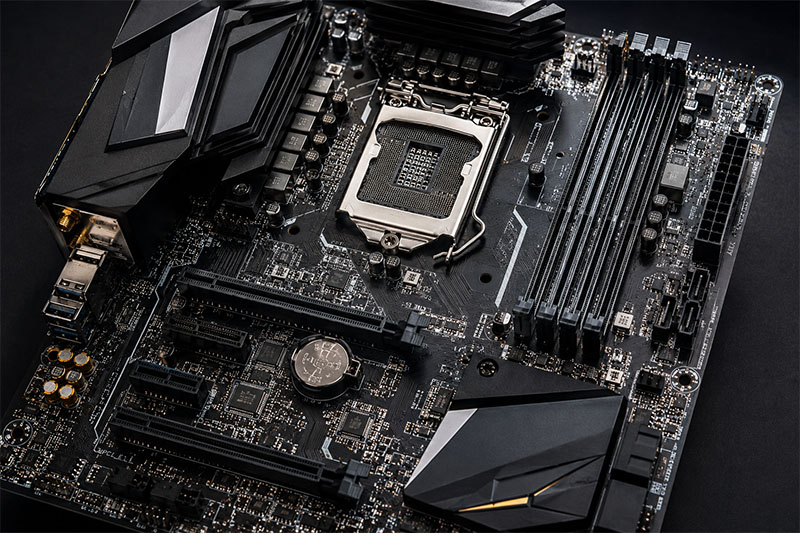
How Does Motherboard Customization Ensure Better Performance?
Motherboard customization is the process of tailoring the PCB’s electrical, physical, and thermal properties to the exact needs of a specific application, which directly translates to superior performance compared to using a generic, off-the-shelf board. This optimization impacts every aspect of the system: speed, power efficiency, thermal behavior, reliability, and form factor. For demanding applications, a custom built motherboard is not a luxury but a necessity to achieve performance benchmarks and gain a competitive edge.
The performance benefits of a custom PC motherboard are realized through targeted design choices across several domains:
- Optimized Signal Integrity and Speed: Customization allows for precise control over the PCB stack-up, dielectric materials, and trace geometry. This enables perfect impedance matching for high-speed signals (e.g., DDR5, PCIe 5.0), minimizing reflections and losses. You can use low-loss laminates (Df < 0.005) in critical paths, which a standard FR4 board does not offer, allowing for higher data rates and lower bit error rates.
- Enhanced Thermal Management: A one-size-fits-all motherboard has generic thermal design. Customization lets you integrate direct thermal solutions. For example, you can specify a thicker copper plane (e.g., 3 oz) under a high-power CPU, incorporate an array of thermal vias to an internal ground plane, or even design a section as a Metal Core PCB (MCPCB) with a thermal conductivity of 2.0-3.0 W/m·K to act as an integrated heatsink, dramatically lowering junction temperatures.
- Superior Power Delivery: Custom power planes can be designed with the exact copper weight and shape needed for each voltage rail, reducing DC resistance (Rdc) and voltage drop. This ensures stable power to sensitive components like FPGAs and GPUs, even under transient loads, preventing throttling and ensuring consistent performance.
- Form Factor and Component Optimization: The board can be shaped to fit a unique enclosure, and components can be placed for optimal mechanical and electrical interaction. This reduces parasitic inductance and capacitance from long traces, improves EMI performance by allowing for better shielding strategies, and can even reduce the overall part count by integrating functions, leading to higher reliability.
In essence, motherboard customization moves the design from a compromise-based generic solution to a purpose-engineered platform. It allows engineers to make deliberate trade-offs that favor the most critical performance parameters of their specific application, whether that’s raw compute speed, power efficiency in a battery-operated device, or rugged reliability in an industrial setting. This tailored approach is what unlocks the full potential of the components mounted on it.
Why Do Complex Projects Need the Best Motherboard Customer Service?
Complex projects involving custom motherboards inherently carry high technical risk, significant investment, and tight schedules. The best motherboard customer service is the essential human and procedural interface that actively manages this risk, provides expert guidance, and ensures smooth project execution. It transforms a manufacturing transaction into a collaborative partnership, where the manufacturer’s team acts as an extension of your own, providing support that is proactive, knowledgeable, and responsive to the unique challenges of a sophisticated custom motherboard build.
Outstanding customer service for a complex motherboard project manifests in several critical, tangible ways:
- Front-Loaded Technical Collaboration (Pre-Sales): Before any order is placed, the service team facilitates deep-dive technical reviews. Their engineers provide a detailed DFM report, not just flagging errors but offering solutions—like suggesting changing a via pad size from 8 mil to 10 mil for better reliability, or recommending an alternative surface finish for a challenging BGA. This prevents costly mistakes from ever reaching production.
- Proactive Supply Chain Management: For a custom motherboard with a large, complex BOM, component sourcing is a minefield. The best service includes a dedicated procurement specialist who proactively communicates about part availability, suggests alternates for end-of-life or long-lead items, and provides a consolidated, optimized BOM list, de-risking your supply chain from the start.
- Real-Time Project Visibility & Communication: You are not left in the dark. A digital portal or regular WIP updates show you the status of your boards at every stage—from PCB lamination and drilling to SMT assembly and testing. If a minor issue arises (e.g., a solder paste issue on the line), you are informed immediately with a solution, not after the fact.
- Rapid-Response Problem Solving: When an unexpected challenge occurs—a last-minute engineering change order (ECO), a test failure that needs diagnostics—the service team provides fast, expert-level troubleshooting. They have direct access to the factory floor and engineering teams to investigate and resolve issues within hours, not days, keeping your project on track.
- Seamless Transition from NPI to Mass Production: The team that guided your prototype ensures all learnings and specifications are perfectly handed over to the volume production group. They manage the transition, ensuring there are no surprises in quality or process when you scale up your order.
For a complex project, this level of service is not a premium add-on; it is a core component of project success. The best custom motherboard manufacturer understands that their value lies as much in their knowledge, communication, and support as in their machinery. This partnership minimizes stress, accelerates time-to-market, and provides the confidence that your intricate, high-stakes project is in capable hands from the first design file to the final shipped unit.
To sum up, custom motherboard PCBs are the engineered heart of high-performance electronic systems, where tailored design and precision manufacturing converge to unlock specific application potential. This article has detailed the journey from optimized layout and critical verification through prototype fabrication and the stringent requirements of mass production, underscoring the importance of choosing a manufacturing partner that acts as a true collaborator.
EBest Circuit (Best Technology) brings over 20 years of PCB and PCBA expertise to this complex field. Our in-house engineering team provides deep DFM analysis for your custom motherboard design, while our one-stop turnkey service—encompassing advanced PCB fabrication, robust component sourcing, and high-mix PCBA assembly—ensures a seamless, accountable process from prototype to volume production. Supported by relevant quality certifications and a digital workshop for full traceability, we are equipped to be your reliable partner in bringing high-performance, reliable custom motherboards to market. Pls feel free to contact our team anytime to discuss your project requirements at sales@bestpcbs.com.
FAQs About Custom Motherboard
Q1: What is the typical lead time for a prototype of a custom motherboard, and can it be expedited?
A: The lead time for a custom motherboard prototype depends on complexity. For a standard 8-layer FR4 design (<1 sq. meter), normal PCB fabrication is about 12 days, with PCBA adding roughly a week. However, with expedited services, the PCB can be built in 72 hours, and fast-turn PCBA can be completed in 2 days, bringing the total project timeline to approximately 1.5 weeks. Manufacturers like EBest Circuit offer such rush services to help accelerate R&D validation cycles.
Q2: What are the key DFM (Design for Manufacturability) checks I should perform on my custom motherboard design before sending it out?
A: Beyond standard ERC/DRC, focus on manufacturer-specific process limits. Key checks include: ensuring trace/space and annular ring sizes meet their standard (e.g., 5/7 mil for 2 oz copper), verifying hole-to-copper clearance (≥0.18mm), avoiding excessive copper in flex areas to prevent cracking, and confirming your impedance stack-up model is achievable with their materials. The most effective step is to request a formal DFM report from your chosen manufacturer, as they will apply their exact equipment and process tolerances to your design.
Q3: How do you handle component sourcing, especially for obsolete or hard-to-find parts on a custom PC motherboard BOM?
A: A reputable turnkey manufacturer manages this through a multi-pronged approach. They first source from a network of authorized distributors to guarantee authenticity. For obsolete parts, their procurement team will identify and suggest qualified, form-fit-function equivalent alternates. They can also leverage in-house inventory of common components. Providing your BOM early allows them to initiate sourcing in parallel with PCB fabrication, mitigating lead time risks. Always ask for a component sourcing report before production begins.
Q4: What is the advantage of using a Metal Core PCB (MCPCB) section in a custom motherboard design?
A: Integrating an MCPCB section, typically aluminum-based, is a powerful thermal management strategy for custom motherboard customization. The metal core acts as an integrated heatsink, conducting heat away from high-power components like VRMs or processors much more efficiently than standard FR4 (thermal conductivity of 1.5-3.0 W/m·K vs. ~0.3 W/m·K). This can lower component operating temperatures significantly, improving reliability and performance, and potentially eliminating the need for bulky external heatsinks in some areas, allowing for a more compact design.
Q5: Can you support both small-batch prototyping and later mass production for the same custom motherboard design?
A: Yes, the best manufacturers are equipped for this full lifecycle support. They use the same certified processes and equipment lines for both prototyping and volume runs, ensuring consistency. The transition is managed by the same engineering and customer service team, who carry over all the learnings and optimized parameters from the prototype phase. This seamless handoff guarantees that the performance and quality you validated in your prototypes are maintained in mass production, which is critical for a custom motherboard manufacturer relationship.