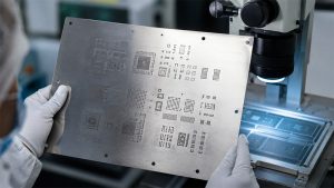
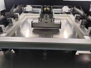
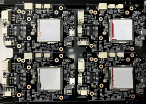
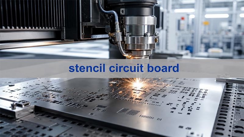
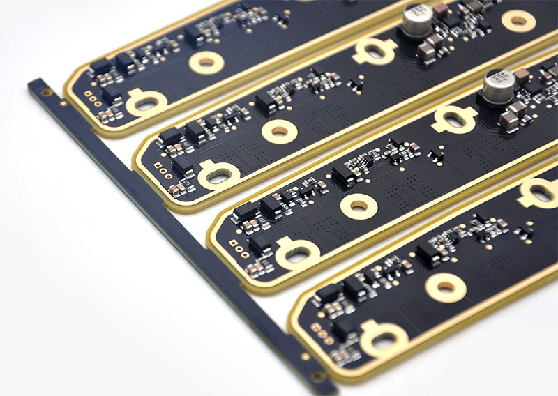
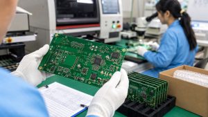
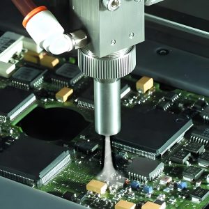
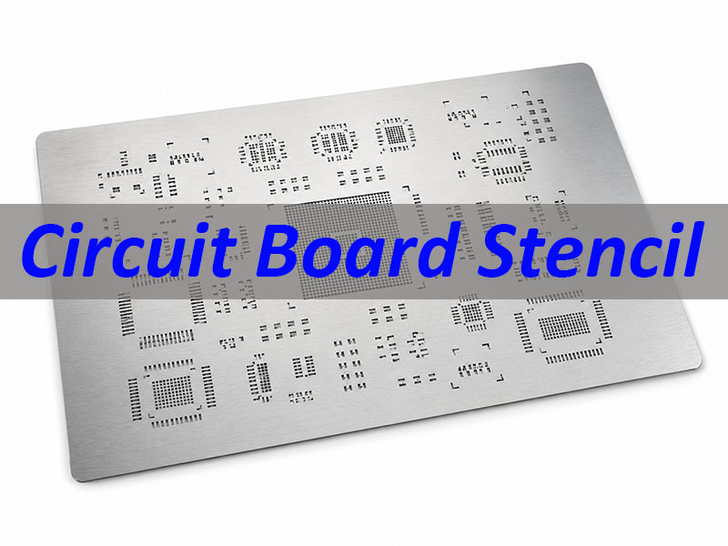
A circuit board stencil is used to print solder paste onto PCB pads before SMT assembly. A good stencil helps control solder paste volume, improve printing accuracy, reduce solder defects, and make PCB assembly more stable.
EBest Circuit (Best Technology), branded as EBEST, can provide circuit board stencils for SMT assembly projects, including laser-cut stencils, etched stencils, framed stencils, frameless stencils, PE stencils, BGA-related stencils, LED PCB stencils, and step-up/step-down stencil options.
For a circuit board stencil quote, please send your Gerber files, PCB files, CAD files, Protel files, stencil size, thickness requirement, framed or frameless preference, quantity, and delivery target to sales@bestpcbs.com.
Can EBEST Provide Circuit Board Stencils for SMT Assembly?
Yes. EBEST can provide circuit board stencils for SMT solder paste printing.
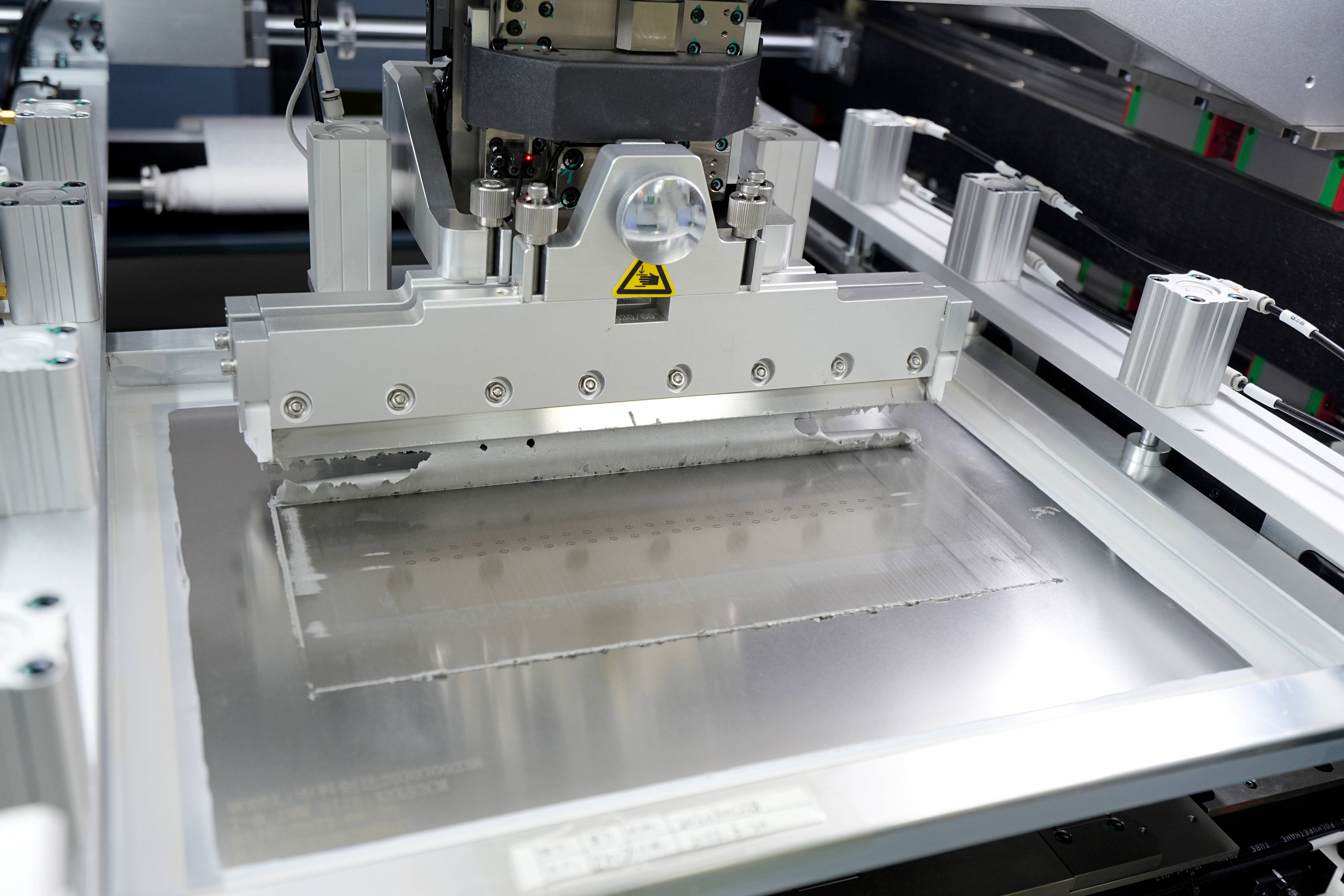
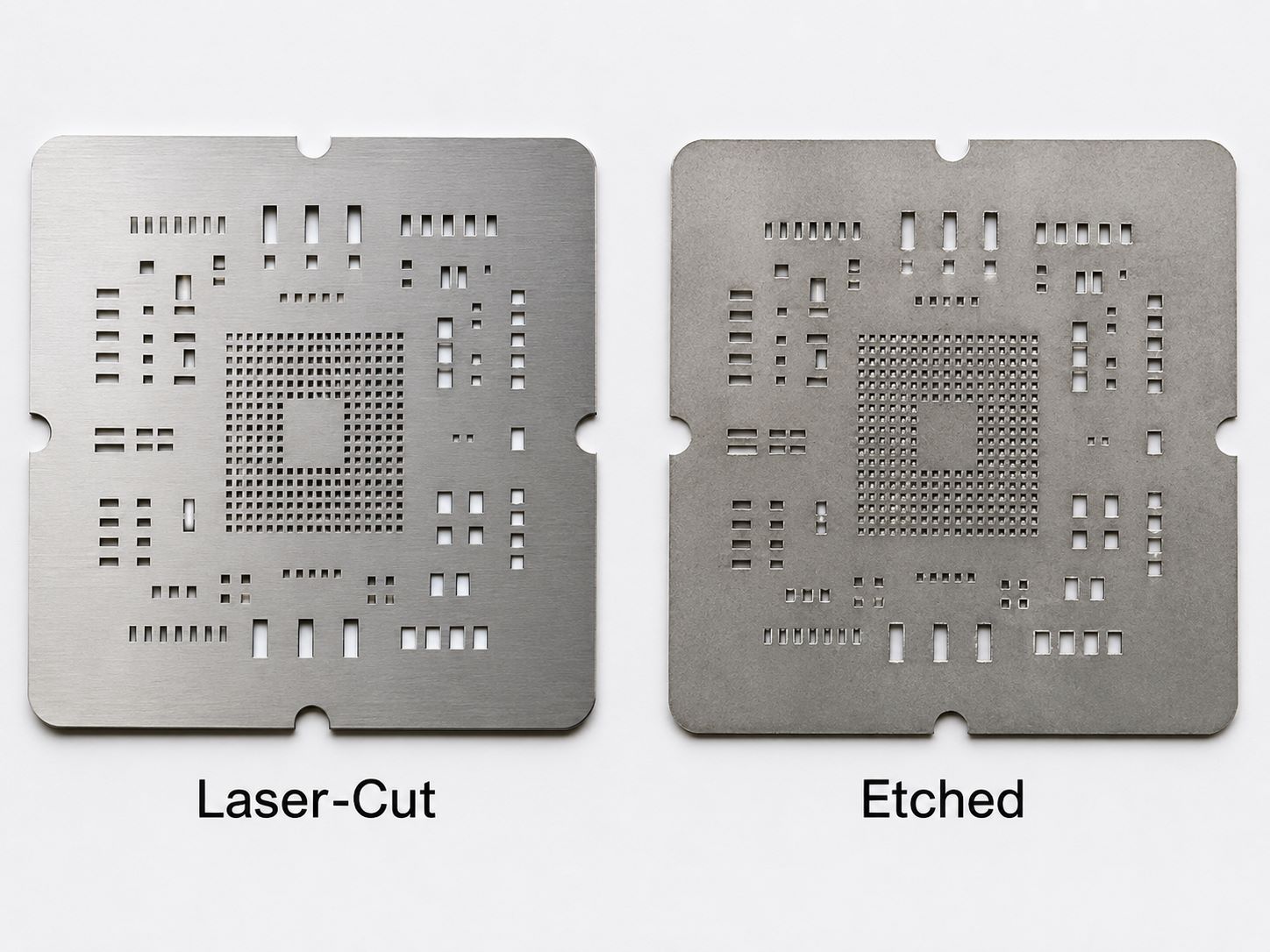
Most EBEST SMT stencils are laser-cut because laser cutting provides better aperture accuracy and smoother paste release for PCB assembly. Etched stencils are also available when the project requirement or budget is more suitable for etching.
EBEST stencil support can be used for:
- Prototype PCB assembly
- Small-batch PCBA projects
- Standard SMT production
- Fine-pitch component assembly
- BGA and QFN assembly support
- LED PCB and metal core PCB assembly
- Custom PCB assembly projects
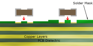
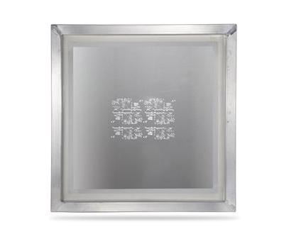
A circuit board stencil helps transfer solder paste to PCB pads through precisely cut openings. If the stencil opening, thickness, or surface quality is not suitable, SMT defects can happen before component placement even starts.
Common problems from poor stencil control include:
- Too much solder paste
- Insufficient solder paste
- Solder bridging
- Solder balls
- Component shift
- Tombstoning
- Poor BGA soldering
- Extra stencil cleaning time
EBEST reviews the stencil requirement together with the PCB assembly need, so the stencil is not treated as a separate accessory but as part of the SMT process.
What Printed Circuit Board Stencils Can EBEST Supply?
EBEST can supply different printed circuit board stencils based on assembly method, board size, component type, and solder paste requirement.
Common stencil options include:
- Laser-cut stainless steel stencil
- Etched stencil
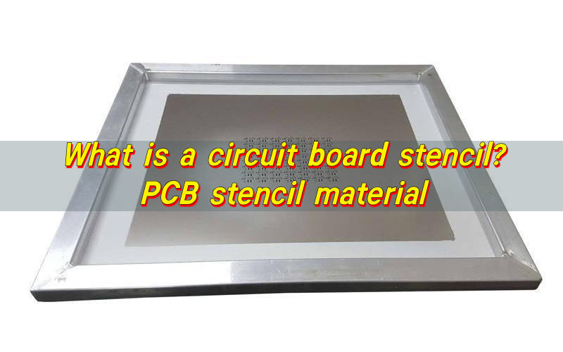
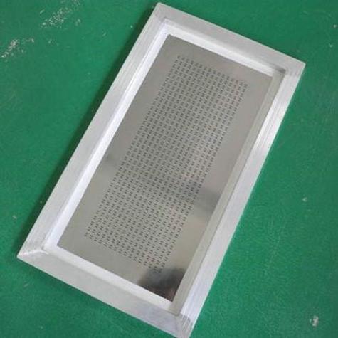
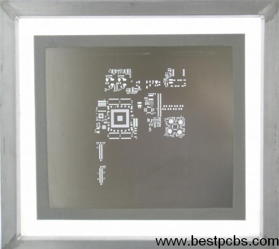
- Framed stencil
- Frameless stencil
- PE stencil
- BGA ball mounting stencil
- Long strip LED stencil
- Metal core PCB stencil
- Step-up and step-down stencil
Most SMT assembly projects use stainless steel stencils because they provide stable strength, good aperture accuracy, and reliable solder paste printing.
Laser-cut stencils are suitable when the project needs:
- Higher aperture accuracy
- Better wall smoothness
- Easier solder paste release
- Fine-pitch component support
- More stable SMT printing
Etched stencils may be considered when:
- The project is cost-sensitive
- The PCB design is not very complex
- The aperture requirement is less demanding
- The order is for simple prototype use
EBEST can also provide fiducial marks on stencil sides when required, which helps align the stencil during solder paste printing.
Laser-Cut or Etched Circuit Board Stencil: Which One Should You Choose?
A laser-cut circuit board stencil is usually the better choice for SMT assembly projects that need stable solder paste printing.
Laser-cut stencils are recommended for:
- Fine-pitch ICs
- BGA components
- QFN packages
- Dense SMT layouts
- Small pads
- High repeatability printing
- Production assembly
Laser cutting helps improve:
- Aperture accuracy
- Solder paste release
- Printing consistency
- Pad opening quality
- SMT efficiency
EBEST laser-cut stencils are electro-polished to improve aperture wall smoothness. Smoother aperture walls help solder paste release more easily, reduce cleaning frequency, and improve printing stability.
Etched stencils can still be useful for:
- Simple boards
- Lower-cost projects
- Basic SMT printing
- Less demanding pad designs
The right choice depends on the PCB layout, component pitch, solder paste volume, budget, and assembly quantity.
For most PCBA projects with fine-pitch components, laser-cut stencil is the safer choice.
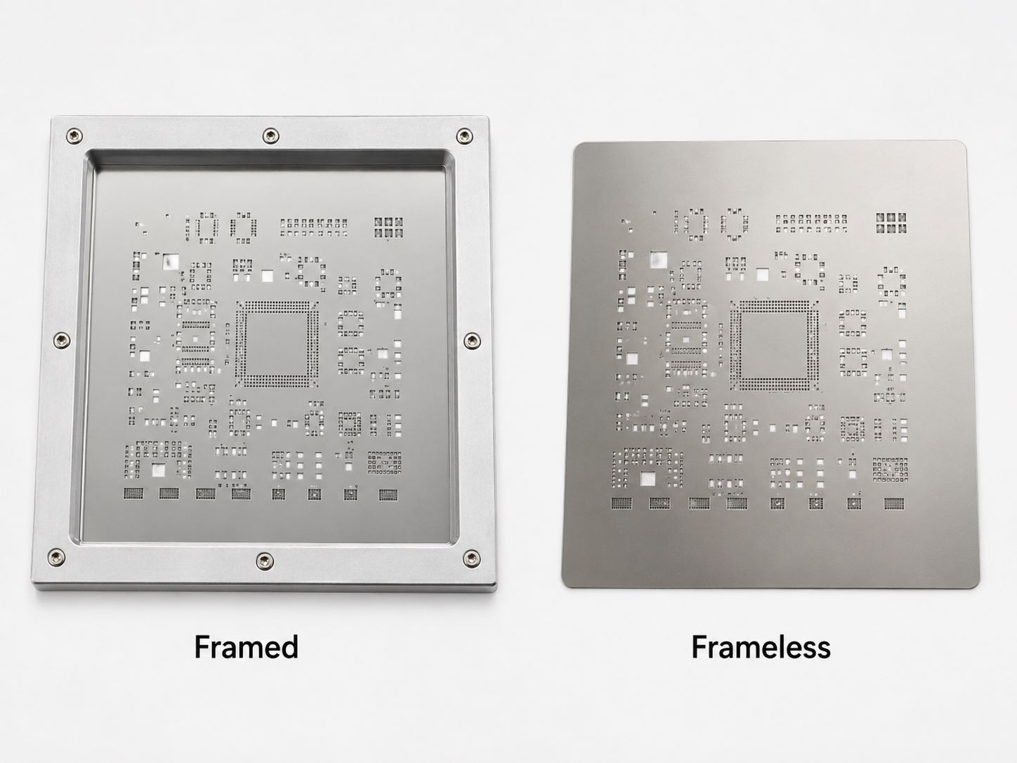
Framed or Frameless PCB Stencil: Which Type Fits Your Assembly?
Both framed and frameless PCB stencils can be used for SMT solder paste printing, but they fit different production needs.
A framed stencil is suitable for:
- Regular SMT production
- Repeated printing
- Higher tension stability
- Standard stencil printer use
- Better handling during production
A frameless stencil is suitable for:
- Prototype assembly
- Small-batch use
- Lower storage space
- Lower shipping weight
- Customers using reusable stencil frames
Framed stencils are more stable during printing because the stencil foil is fixed inside a frame. This helps maintain tension and alignment during repeated use.
Frameless stencils are more flexible for prototype and low-volume projects, especially when customers want to reduce shipping cost or use their own frame system.
For large circuit board stencil projects, long strip LED boards, or large panel SMT printing, framed stencil is often safer because it gives better support during printing.
EBEST can review the stencil type based on:
- PCB size
- Panel size
- Assembly quantity
- Stencil printer type
- Shipping requirement
- Customer production method
How Does Stencil Thickness Affect SMT Solder Paste Printing?
Stencil thickness affects solder paste volume.
If the stencil is too thick, too much solder paste may cause bridging, solder balls, or component floating. If the stencil is too thin, insufficient solder paste may cause weak solder joints or open circuits.
Common EBEST stencil thickness options include:
- 0.10mm
- 0.12mm
- 0.15mm
- Custom thickness up to 0.60mm
General selection logic:
- 0.10mm: Fine-pitch parts, small pads, and compact SMT designs
- 0.12mm: Fine-pitch and mixed SMT layouts
- 0.15mm: Common SMT assembly and general-purpose PCBA
- Thicker stencil: Larger pads, power components, connectors, or special solder paste volume needs
Stencil thickness should be checked together with:
- Smallest pad size
- Component pitch
- BGA or QFN area
- Connector pads
- LED pads
- PCB surface finish
- Solder paste type
- Assembly quantity
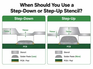
Some projects need different solder paste volume in different areas. In that case, a step-up or step-down stencil may be a better option than using one uniform thickness for the whole board.
What Custom Stencil Options Can EBEST Support?
EBEST can support custom stencil options when a standard stencil cannot meet the solder paste requirement.
Available custom options include:
- Step-up stencil
- Step-down stencil
- BGA ball mounting stencil
- Long strip LED stencil
- Metal core PCB stencil
- PE stencil
- Custom aperture scaling
- Local thickness control
- Fiducial mark support
- Tapered aperture wall design
Step-up and step-down stencils are used when different PCB areas need different solder paste volumes.
For example:
- Normal components may use a 1:1 opening scale.
- BGA areas may use a reduced scale such as 0.9:1.
- Larger pads may need more solder paste.
- Fine-pitch areas may need less solder paste to reduce bridging.
Long strip LED stencils are useful for LED PCB and metal core PCB assembly, where board length, thermal pad design, and paste consistency can affect production quality.
BGA ball mounting stencils are used for BGA-related assembly or repair support, where ball position and opening accuracy matter.
PE stencils can be used for certain prototype or special-use cases where a metal stencil is not the best fit.
Custom stencil selection should always follow the PCB layout and assembly process, not only the stencil price.
What Files Are Needed for a Circuit Board Stencil Quote?
A correct stencil quote needs the right files and specifications.
Please send:
- Gerber files
- PCB file or CAD file
- Protel file, if available
- Paste layer file
- PCB size
- Panel size
- Stencil size
- Framed or frameless requirement
- Stencil thickness
- Laser-cut or etched preference
- Fiducial mark requirement
- Step-up or step-down requirement, if needed
- Special aperture notes
- Quantity
- Delivery target
- Shipping address or destination country
For PCBA projects, please also provide:
- BOM
- Pick-and-place file
- Assembly drawing
- Component package notes
- Fine-pitch or BGA information
- Solder paste requirement
- SMT production requirement
Direct data input from customer electrical files helps reduce manual errors. Gerber, PCB, CAD, and Protel files are useful because they allow the stencil openings to follow the actual PCB paste layer.
Before making the stencil, EBEST may check:
- Aperture size
- Pad opening ratio
- Fiducial marks
- PCB panelization
- Fine-pitch areas
- BGA or QFN areas
- Large pad solder paste volume
- Framed or frameless choice
- Shipping packaging needs
Clear files lead to a faster quote and fewer stencil problems.
FAQs About Circuit Board Stencil
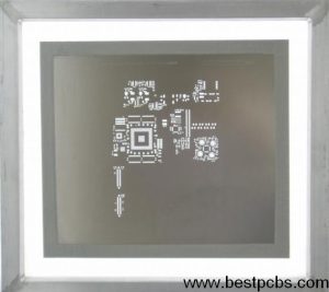
What Is a Circuit Board Stencil?
A circuit board stencil is a thin template used to print solder paste onto PCB pads before SMT assembly. It is also called a PCB stencil, SMT stencil, or solder paste stencil.
Is a Circuit Board Stencil the Same as a PCB Stencil?
Yes. In PCB assembly, circuit board stencil, PCB stencil, SMT stencil, and solder paste stencil usually refer to the same tool used for solder paste printing.
Does “Stencil Circuit Board” Mean the Same Thing?
“Stencil circuit board” is not the most accurate engineering term. Most buyers who search this phrase usually mean a circuit board stencil or PCB stencil for SMT solder paste printing.
What File Is Needed to Make a PCB Stencil?
The paste layer from Gerber files is usually needed to make a PCB stencil. PCB files, CAD files, Protel files, panel drawings, and assembly notes can also help confirm the stencil design.
What Stencil Thickness Should I Choose?
Common stencil thickness options include 0.10mm, 0.12mm, and 0.15mm. The right choice depends on pad size, component pitch, solder paste volume, BGA or QFN areas, and assembly requirements.
Can EBEST Provide Both Framed and Frameless Stencils?
Yes. EBEST can provide framed and frameless circuit board stencils based on customer production needs, stencil printer setup, shipping method, and assembly quantity.
Can EBEST Provide Laser-Cut Stencils?
Yes. Most EBEST SMT stencils are laser-cut, and electro-polishing is available to improve aperture wall smoothness and solder paste release.
How Do You Cover Unused Holes in a Circuit Board Stencil?
Unused apertures, or “holes,” in a circuit board stencil can sometimes be covered temporarily with high-temperature tape during prototype solder paste printing. This is only a short-term solution. For stable SMT production, it is better to modify the paste layer file or make a new stencil, because covered apertures may cause solder paste leakage, contamination, uneven printing, or extra cleaning.
Do All PCBA Projects Need a Stencil?
Most SMT assembly projects need a stencil because solder paste must be printed accurately before component placement. Some hand-soldered or very simple prototype projects may not need one, but stencil printing is more stable for repeatable SMT assembly.
Can EBEST Provide Stencil Support Together with PCBA Assembly?
Yes. EBEST can provide stencil support together with PCBA assembly, including PCB fabrication, stencil preparation, SMT assembly, DIP assembly, inspection, and functional testing when required.
To sum up, a circuit board stencil is a small part of the SMT assembly process, but it has a direct effect on solder paste printing quality.
The right stencil can help reduce solder bridges, insufficient solder, solder balls, component shift, and repeated cleaning during SMT production.
EBEST can provide circuit board stencils for SMT PCB assembly, including laser-cut stencils, etched stencils, framed stencils, frameless stencils, PE stencils, BGA-related stencils, LED PCB stencils, and step-up/step-down stencil options.
For a circuit board stencil quote, please send your Gerber files, PCB files, CAD files, Protel files, stencil size, thickness requirement, framed or frameless preference, quantity, and delivery target to sales@bestpcbs.com.