Why Choose EBest for Single Sided PCB Manufacturing?
EBest is your top choice for single sided PCB manufacturing, delivering consistent quality, fast lead times, and expert support for both prototypes and mass production. We focus on reliability and precision for every order.
- Lead Time: Fast turnaround for prototypes and volume orders; on-time delivery guaranteed.
- Quality: IPC-compliant production with strict inspection to ensure zero defects.
- Certifications: ISO 9001 and RoHS compliant, with full material traceability.
- Support: Free DFM (Design for Manufacturing) analysis and no minimum order quantity for prototypes.
- Service: 24/7 engineering support and dedicated account managers to assist with your project.
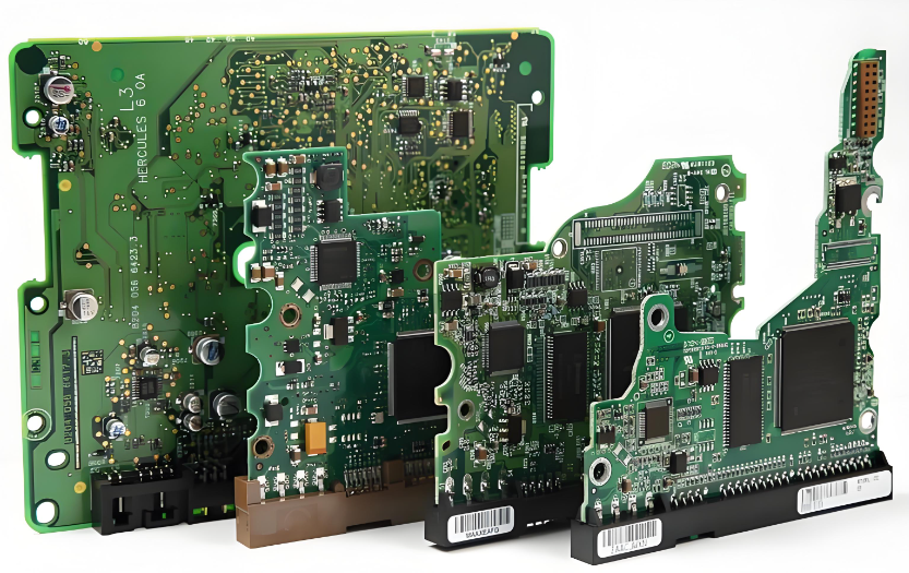
What Is a Single Sided PCB?
A single sided PCB (single-layer PCB) is a printed circuit board with one conductive copper layer on one side of an insulating substrate. Components are mounted on the top side, while all traces, pads, and connections are located on the bottom copper layer. It is the simplest and most cost-effective PCB type, ideal for low-complexity, high-volume electronic devices.
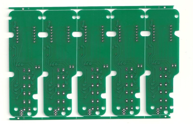
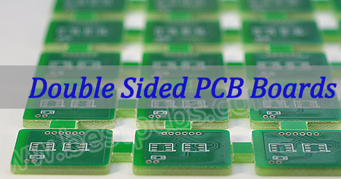
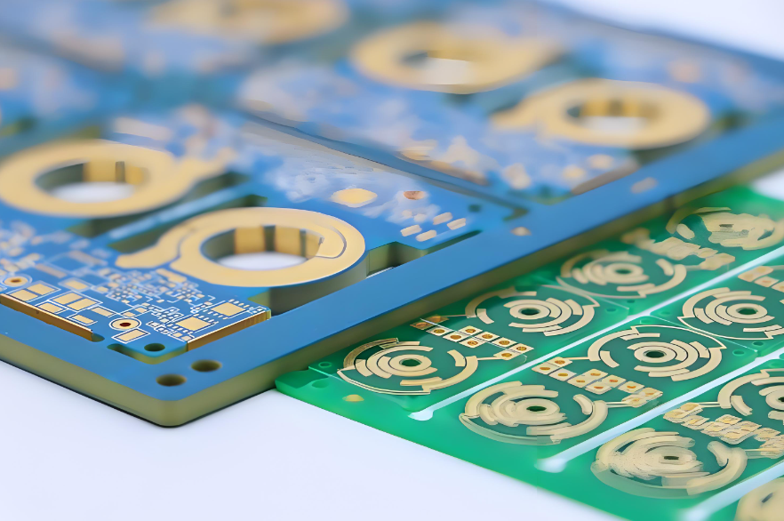
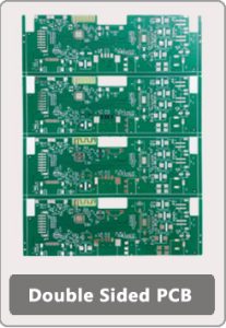
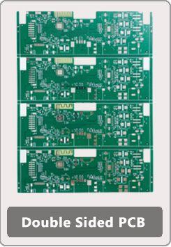
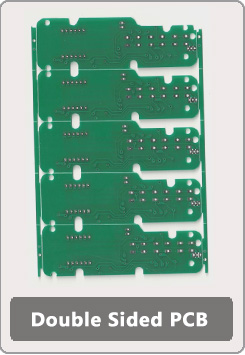
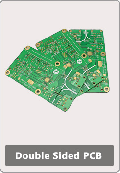
Single Sided PCB
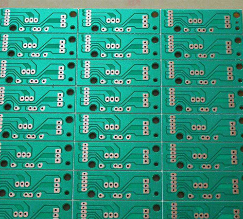
Single Sided PCB Manufacturing Process
The production of a single sided PCB follows a precise, streamlined process to ensure quality and consistency:
- Material Preparation: Cut the copper-clad laminate (CCL) to the required panel size.
- Cleaning & Drilling: Clean the panels thoroughly, then drill mounting holes and tooling holes.
- Pattern Transfer: Apply photoresist to the copper layer, then expose and develop it to define the circuit traces.
- Etching: Remove excess copper from the panel, leaving only the desired conductive pattern.
- Solder Mask & Silkscreen: Apply a green solder mask (standard) to protect the traces, then add component labels and logos via silkscreen.
- Surface Finish & Testing: Apply a surface finish (HASL as standard, or immersion tin as an option) and perform electrical continuity and isolation tests to ensure functionality.
- Routing & Inspection: Route individual PCBs from the panel and conduct a final visual and dimensional inspection to meet quality standards.
Single Sided PCB Design Guide: Rules & Best Practices
Designing single sided PCBs is straightforward but requires strict adherence to rules to avoid errors. The biggest challenge is trace routing without vias, as all connections must fit on a single copper layer.
What Are the Main Design Pain Points?
- Trace Routing: Vias are not allowed, making it easy to create loops or unintended crossovers.
- Space Limitations: Dense component placement leaves little room for trace routing.
- Noise Interference: Long, parallel traces increase the risk of electromagnetic interference (EMI).
- Pad Spacing: Small pad sizes increase the risk of short circuits during soldering.
How Does EBest Solve These Issues?
Our engineers provide free DFM reviews to optimize your PCB layout, including:
- Using ground planes on unused copper areas to reduce EMI and improve signal integrity.
- Routing traces perpendicularly to each other to avoid crossovers and signal interference.
- Widening power and ground traces to accommodate higher current capacity and prevent overheating.
- Adding test points to simplify debugging and quality testing.
For expert single sided PCB design support, trust EBest.
Premium Single Sided PCB Prototypes: Fast & Reliable
Single sided PCB prototypes are critical for validating designs before mass production. Engineers often face delays, poor quality, or design mismatches when working with generic suppliers.
Key Prototype Pain Points
- Slow Turnaround: Long wait times for prototypes delay testing and project timelines.
- Design Errors: Misinterpreted design specifications lead to rework and additional costs.
- Material Issues: Subpar substrates and copper layers compromise prototype performance and reliability.
- Testing Gaps: Lack of pre-shipment quality checks results in prototype failures during testing.
EBest’s Prototype Solution
We deliver high-quality single sided PCB prototypes with:
- 24–48 hour turnaround for standard designs (expedited options available).
- 1:1 design fidelity, strictly adhering to IPC standards and your design specifications.
- Premium substrates (FR-1, CEM-1, FR-4) to ensure stability and performance.
- Pre-ship testing (continuity and short-circuit checks) to guarantee functionality.
For fast, reliable single sided PCB prototypes, choose EBest.
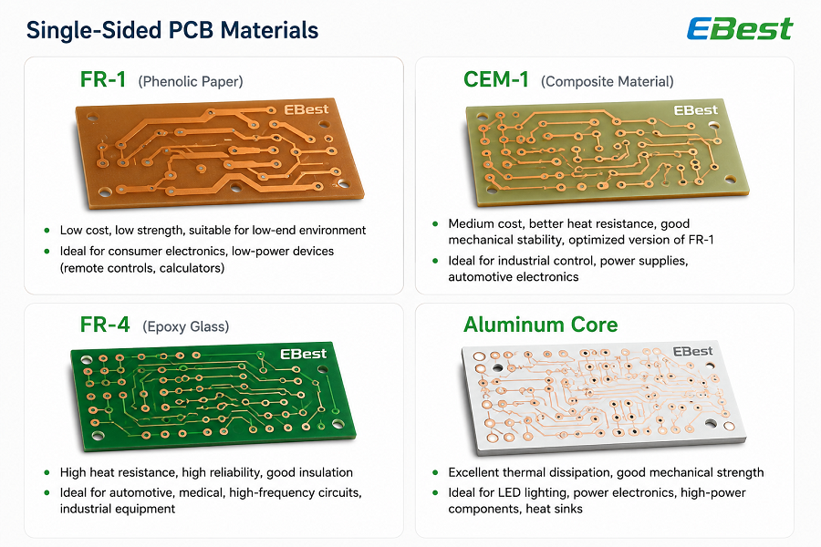
How to Select Raw Materials for Single Sided PCBs?
Material selection directly impacts the performance, durability, and functionality of a single sided PCB. Below are common materials and their key specifications, tailored to different applications.
| Material Type | Key Features | Best For |
|---|---|---|
| FR-1 (Phenolic Paper) | Low cost, flame retardant, rigid, suitable for low-temperature applications | Consumer electronics, low-power devices (remote controls, calculators) |
| CEM-1 (Composite) | Mid-range cost, improved heat resistance, better mechanical stability than FR-1 | Industrial controls, power supplies, basic automotive electronics |
| FR-4 (Epoxy Glass) | High heat resistance, excellent reliability, good electrical insulation | Automotive, medical, high-frequency circuits, industrial equipment |
| Aluminum Core | Exceptional heat dissipation, lightweight, rigid | LED lighting, power electronics, high heat generation devices |
Single Sided PCB Datasheet Highlights
- Board Thickness: 0.6mm–1.6mm (standard: 1.0mm; custom thicknesses available)
- Copper Weight: 1oz (35μm) standard; 2oz (70μm) available upon request
- Solder Mask: Green (standard); red, blue, black custom options
- Surface Finish: HASL (standard); immersion tin or gold flash optional
What Are the Common Applications of Single Sided PCBs?
Single sided PCBs are widely used across diverse industries due to low cost, simplicity, and reliability. Four key sectors include:
- Consumer Electronics: Remote controls, calculators, toys, small home appliances.
- Industrial Control: Sensors, relays, power supplies, motor drivers, automation equipment.
- Automotive: Interior lighting, dashboard controls, door locks, simple ECUs.
- LED Lighting: LED strips, drivers, bulb circuits (aluminum core for heat dissipation).
What Are the Key Design Challenges for Single Sided PCBs?
The biggest hurdle in single sided PCB design is 100% surface routing without vias, limiting layout flexibility. Other challenges:
- Crossover Avoidance: Traces cannot cross; careful planning required for single-layer routing.
- High-Density Layouts: Limited space for components and traces.
- EMI/EMC Compliance: Uncontrolled routing causes electromagnetic interference.
- Thermal Management: Basic substrates offer limited heat dissipation.
How to Avoid Common Mistakes in Single Sided PCB Layout?
Follow these best practices to eliminate errors in single sided PCB design:
- Plan Routing First: Sketch paths before component placement.
- Minimize Trace Lengths: Shorter traces reduce resistance and noise.
- Use Ground Planes: Improve signal integrity and reduce interference.
- Avoid 90° Angles: Use 45° angles to prevent etching and signal issues.
- Widen High-Current Traces: Prevent overheating and voltage drops.
What Quality Standards Apply to Single Sided PCBs?
Single sided PCBs meet strict industry standards for reliability and safety:
- IPC-2221: Generic PCB design standard
- IPC-6011: PCB performance specification
- RoHS: Lead-free, environmentally friendly production
- ISO 9001: Quality management certification
- UL 94 V-0: Flame retardancy for safety-critical applications
FAQ: Common Questions About Single Sided PCBs
Q1: What is the maximum size for a single sided PCB?
A1: Standard panels up to 1200mm × 1000mm; custom sizes available.
Q2: Can single sided PCBs be used for high-frequency circuits?
A2: Yes, with FR-4 or PTFE substrates. Keep traces short and maintain controlled impedance.
Q3: What is the minimum trace width and spacing for single sided PCBs?
A3: Standard: 0.2mm / 0.2mm. Advanced: 0.1mm / 0.1mm.
Q4: Are single sided PCBs RoHS compliant?
A4: Yes, all EBest single sided PCBs are RoHS compliant with lead-free finishes.
Q5: What is the typical lead time for mass production?
A5: 7–10 business days for standard orders; expedited service available.
Get Your Custom Single Sided PCB from EBest Today
EBest is your trusted partner for high-quality single sided PCBs, from prototypes to mass production. We provide precision manufacturing, expert support, and reliable delivery.
Contact us for a free quote: sales@bestpcbs.com
Let’s build your next single sided PCB with EBest.