PCB manufacturing PCB manufacturing
Home > Blog

Ethernet PCB

Ethernet PCB Manufacturing and Assembly for Network Hardware
Monday, September 21st, 2026

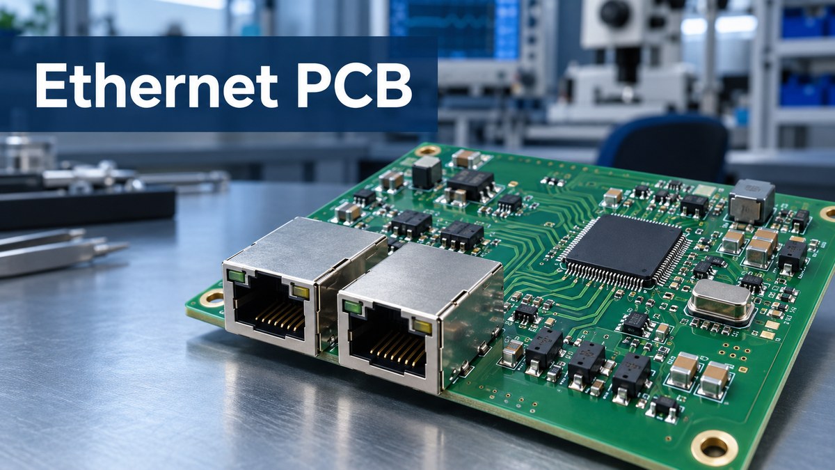
An Ethernet PCB that links reliably on a laboratory bench can still become unstable in production if the fabricated stackup, connector assembly, or test method differs from the released design. Link speed, PHY interface, isolation magnetics, connector style, PoE requirements, and the enclosure all affect how the board must be laid out, fabricated, assembled, and verified.

EBest Circuit turns customer-approved schematics and component requirements into manufacturable layouts, controlled-impedance PCBs, and assembled network boards. With in-house PCB and PCBA production, 20 years of PCBA experience, and a supply network of more than 1,000 partners, we can coordinate fabrication, component sourcing, SMT and through-hole assembly, and agreed testing under one production route. To discuss an Ethernet hardware build, contact sales@bestpcbs.com.
Ethernet PCB

How Link Speed Changes Ethernet PCB Requirements

Higher Ethernet speeds leave less margin for insertion loss, crosstalk, discontinuities, and timing variation. The target speed must therefore be fixed before the stackup, magnetics, connector, and test method are released.

Link speedPCB impactBuild priority
10 / 100MTwo active MDI pairsCorrect pair geometry and matched interface parts
1GFour bidirectional pairsFour-pair consistency and 1G link testing
2.5G-10GTighter loss, crosstalk, and thermal limitsMaterial and stackup matched to the PHY budget

The cable-side MDI pairs are not the same as the MAC-to-PHY interface. MII, RMII, RGMII, SGMII, and other system-side interfaces use different electrical and timing rules. For example, RGMII timing depends on the selected MAC, PHY, and internal-delay settings; it should not receive a generic length-compensation rule copied from another design.

PoE adds another layer. The data rate may be correct while the board still has inadequate current capacity, magnetics rating, isolation, or thermal performance. PSE or PD role, PoE type, supply path, copper area, and expected temperature must be defined with the approved circuit.

Where Ethernet PCBs Are Used in Industrial and Embedded Equipment

Ethernet PCBs are used wherever equipment needs a stable wired link, but the board requirements change with the environment and the job performed by the port.

  • Industrial controllers and gateways: PLC interfaces, HMIs, remote I/O, and edge gateways may combine Ethernet with noisy power stages, long field cables, and metal enclosures. Grounding, isolation, surge protection, and connector retention become as important as the PHY itself.
  • Machine vision and IP cameras: A compact board may need high data throughput and PoE in the same interface. Connector position, heat around the PHY and power stage, and repeatable link testing are common production concerns.
  • Embedded computers and test equipment: These boards often combine Ethernet with processors, memory, USB, wireless modules, and sensitive analog sections. Placement and return-current planning must prevent one interface from disturbing another.
  • Switches, access points, and network appliances: Multiple ports increase pair density, power demand, connector alignment, and test coverage. The production fixture and test plan must reflect the actual port count and target speed.

Not every industrial Ethernet port uses an RJ45. Sealed M12 interfaces and single-pair Ethernet use different pin assignments, coupling arrangements, and mechanical constraints. Automotive 100BASE-T1 or 1000BASE-T1, for example, should not inherit a four-pair RJ45 layout merely because both are called Ethernet.

Ethernet PCB Layout Support Based on Customer-Approved Schematics

EBest Circuit can support PCB layout after the customer has approved the network architecture, schematic, PHY, magnetics, connector, and functional requirements. Our role is to translate those decisions into a board that can be fabricated and assembled consistently, not to replace the customer's circuit or system design authority.

  • Physical signal path: Place the PHY, discrete magnetics or magjack, protection parts, and connector so the MDI pairs remain short, balanced, and free of unnecessary stubs and vias.
  • Interface-specific routing: Apply the selected PHY's data sheet and reference design to the MDI path, while treating MII, RMII, RGMII, or serial MAC-side interfaces according to their own timing and impedance requirements. Detailed Ethernet PCB routing rules are reviewed against the actual device rather than copied as universal numbers.
  • Reference and isolation structure: Coordinate reference planes, isolation gaps, chassis or shield connections, and any keepout beneath magnetics with the approved safety and EMC concept.
  • Support circuitry: Keep the oscillator or crystal, bias resistor, decoupling network, termination, and ESD parts in the locations required by the selected components.
  • Manufacturing handoff: Align the net classes and critical geometry with a producible stackup, then return material or geometry changes for approval before CAM release.

The customer remains responsible for PHY and MAC selection, circuit function, firmware, system compliance, and final product validation. This boundary keeps layout support practical without allowing production changes to alter the approved design intent.

How Stackup, Materials, and Controlled Impedance Shape Ethernet PCB Manufacturing

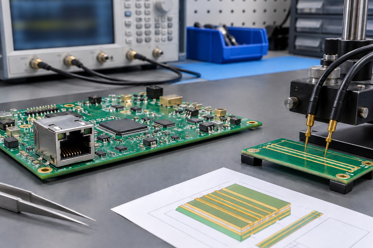
Controlled impedance is a property of the finished stackup, not a trace-width value in isolation. Dielectric thickness and Dk, finished copper, line width and spacing, reference planes, solder mask, and etching compensation work together to produce the result.

For an Ethernet production build, EBest Circuit can support multilayer rigid PCB fabrication from 1 to 32 layers, controlled impedance, and standard or high-Tg FR-4 options; HDI or other special structures are evaluated against the released design. FR-4 is not automatically unsuitable for a faster link, but the selected material and geometry must satisfy the PHY's actual channel-loss budget.

The manufacturing sequence should remain controlled:

  • the customer defines the target impedance and tolerance for each applicable net class;
  • EBest Circuit proposes a manufacturable stackup and calculates the corresponding geometry;
  • the approved material family, dielectric, copper, line width, spacing, via structure, and reference planes are locked for production; and
  • an impedance coupon and TDR record can be supplied when included in the order requirements.

Our impedance control PCB process can verify representative fabricated geometry, but a coupon does not prove the performance of the complete assembled Ethernet channel. Magnetics, connector transitions, soldering, firmware, cable, and link partner still require the appropriate assembly or functional test.
Ethernet PCB

Ethernet PCB Assembly for PHYs, Magnetics, and Network Connectors

Ethernet PCB assembly must hold both the electronic and mechanical interfaces to the released design. A board can have correct copper and still fail if a PHY has hidden-joint defects, a connector sits unevenly, or an unapproved magnetics substitute changes bandwidth, isolation, pinout, or PoE current capacity.

  • BOM and revision control: Source the exact approved PHY, oscillator, magnetics or magjack, connector, ESD device, bias and termination parts, and PoE components. Alternatives require engineering approval; matching only the package or nominal function is not enough.
  • Fine-pitch assembly: Use an appropriate stencil and reflow profile for QFN, BGA, LGA, or other bottom-terminated PHY packages. SPI, AOI, and X-ray are applied where they match the package and inspection plan.
  • Network connector assembly: RJ45, M12, and other ports may use SMT, through-hole, pin-in-paste, or mixed processes. The Ethernet connector PCB build must control seating height, board-edge position, shield tabs, through-hole fill, and the mechanical load transferred from the cable.
  • Integrated or discrete magnetics: A magjack already contains the magnetics, while other designs place a separate transformer between the PHY and connector. The assembly route and inspection points must follow the actual architecture rather than assume both parts are present.

A typical build route is approved BOM verification, solder-paste inspection, SMT placement and reflow, AOI or X-ray as required, through-hole connector assembly, cleaning, and customer-defined testing. PoE boards also need process control for higher-current paths, power devices, isolation areas, and local heat.

Ethernet PCB Inspection and Testing for Bare Boards and PCBAs

No single test proves that an Ethernet board is ready for the end product. Each stage answers a different question, so bare-board, assembly, and link evidence must not be treated as interchangeable.

Test processMain fault foundProduction role
Bare-board electrical testOpens and shortsScreens PCB connectivity before assembly
Coupon / TDRImpedance deviationMonitors stackup and trace geometry
SPI / AOI / X-rayPaste, placement, and solder defectsControls assembly workmanship
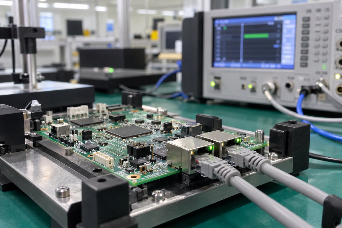
Defined link testPower-up, negotiation, and packet faultsExercises the agreed PCBA functions

These methods address different production layers: electrical testing and TDR cover the fabricated PCB, inspection controls assembly workmanship, and link testing exercises the agreed PCBA functions. EBest Circuit can run customer-defined link tests using approved firmware, fixtures, link partners, and pass/fail limits. Production testing does not replace EMC, safety, PoE, or IEEE compliance validation.
Ethernet PCB

How EBest Circuit Supports Ethernet PCB Prototypes and Repeat Production

EBest Circuit uses prototype builds to establish a manufacturing baseline, then carries the approved data and process into repeat production.

  • Prototype build: DFM and CAM data, stackup, impedance classes, BOM, first-article inspection, and the test method are aligned before release.
  • Repeat orders: Gerber or ODB++, material, stackup, approved alternatives, placement data, firmware, and test revisions remain tied to the order.
  • Traceability: The digital shopfloor can locate material and product-batch records within five seconds when an engineer needs to investigate a component, revision, or lot.
  • In-house execution: PCB fabrication, sourcing, mixed SMT and through-hole assembly, and final inspection follow one coordinated production route. Prototype and small-batch builds are supported.
  • Quality systems: Company certifications include ISO 9001, ISO 13485, IATF 16949, and AS9100D for applicable regulated programs.

FAQs About Ethernet PCB

Does every Ethernet PCB use 100-ohm differential impedance?

Most cable-side copper Ethernet MDI pairs use the differential impedance specified by the PHY and magnetics interface, commonly 100 ohms. MAC-side interfaces, single-pair Ethernet, and vendor-specific structures may follow different requirements, so the selected device data and approved stackup remain the authority.

Can standard FR-4 support a Gigabit Ethernet PCB?

Yes, standard FR-4 is suitable for many 1G boards when the route length, stackup, geometry, and connector path stay within the PHY channel budget. Faster links or longer on-board channels may require tighter loss control or a lower-loss material.

Should the Ethernet magnetics be integrated into the RJ45 or placed separately?

Both architectures are valid. A magjack can shorten the interface path and reduce the part count, while discrete magnetics can provide more flexibility for connector choice, placement, isolation, and PoE implementation. The PCB and assembly route should follow the approved architecture and BOM.

Why can a PCB pass bare-board electrical testing but still fail Ethernet link testing?

Bare-board electrical testing finds opens and shorts; it does not exercise the assembled channel. Link failure can still come from impedance deviation, solder defects, an incorrect component, clock or power problems, PHY configuration, firmware, the connector, or the cable.

Can EBest Circuit perform Ethernet link testing before shipment?

Yes, when the firmware, fixture, link partner, target speed, active ports, and pass/fail limits are agreed before production. The test can cover power-up, link negotiation, and defined packet functions within the approved test scope.

When your schematic and interface architecture are approved, EBest Circuit can coordinate controlled-impedance PCB fabrication, sourcing, assembly, and the agreed link test. Send the released files, target quantity, and test requirements to sales@bestpcbs.com, or arrange an on-site factory audit before first articles or repeat production.


You may also like

Custom PCB Design for Industrial Networks
Saturday, July 11th, 2026
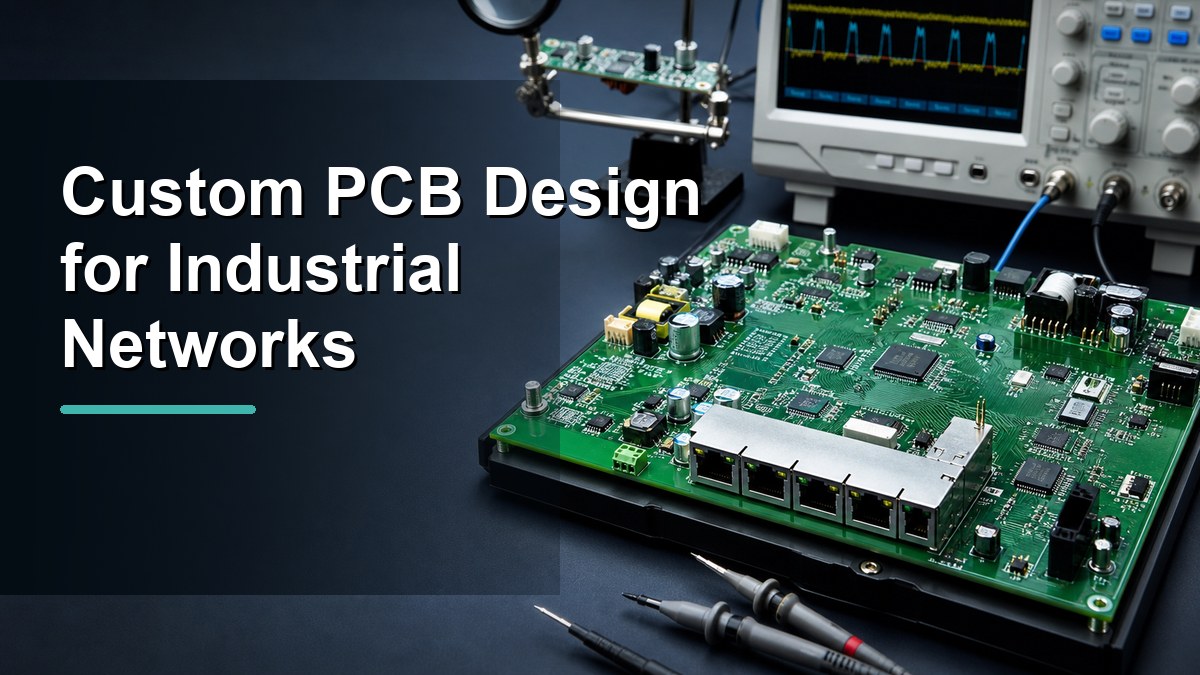
Custom PCB design for industrial networks with Ethernet connectors on an engineering test bench
Industrial network PCB design should be reviewed around signal integrity, power, EMC, connector reliability, and production files before release.

Custom PCB design for industrial networks means building a printed circuit board for reliable data communication in machines, controllers, gateways, sensors, and field devices. The board must handle Ethernet or other network signals, stable power, EMC risk, connector stress, surge exposure, thermal load, and production repeatability at the same time.

For buyers and hardware engineers, the practical question is not only whether the circuit works on the bench. The real question is whether the PCB can be fabricated, assembled, tested, and used in a noisy industrial environment without repeated layout changes. That is why this article focuses on design checks, manufacturing files, and supplier review points for industrial network PCB projects.

What Is Custom PCB Design for Industrial Networks?

Custom PCB design for industrial networks is the process of creating a circuit board layout for devices that exchange data in factory, automation, monitoring, or machine-control environments.

These boards may support industrial Ethernet, RS-485, CAN, PoE, wireless modules, sensor interfaces, edge controllers, gateways, or mixed-signal control circuits. Unlike a generic development board, a custom industrial network PCB must fit the product enclosure, connector position, cable strain, operating temperature, power budget, and final assembly process.

The design work usually starts from schematic and layout, but it should not end there. The PCB also needs stackup definition, impedance planning, connector footprint control, ESD and surge protection, test access, and a manufacturable release package. For projects that need custom board types, review the available custom PCB and PCBA solutions early instead of waiting until the layout is already locked.

Where Industrial Network PCBs Are Used

Industrial network PCBs are used wherever electronic equipment must communicate reliably with other devices under electrical noise, vibration, temperature variation, or long cable runs.

Application Typical board requirement Main design risk
PLC and I/O modules Ethernet, RS-485, isolated inputs, dense connectors Noise coupling, connector spacing, test access
Industrial gateways Multiple RJ45 ports, MCU or MPU, power regulation Impedance control, heat, ESD path
Smart sensors Sensor front end, wireless or wired data link, compact shape Analog noise, grounding, enclosure fit
PoE devices Ethernet data and power on the same cable Power loss, isolation, surge protection
Machine vision or control boards High-speed data, stable power rails, edge connectors Signal integrity, thermal rise, BOM stability

These applications often combine digital communication, power conversion, and field wiring on one board. That combination is useful, but it also creates design conflicts. The layout must keep noisy switching loops away from magnetics and data traces, give connectors enough mechanical support, and leave enough room for inspection and rework.

Key Design Checks Before Layout Release

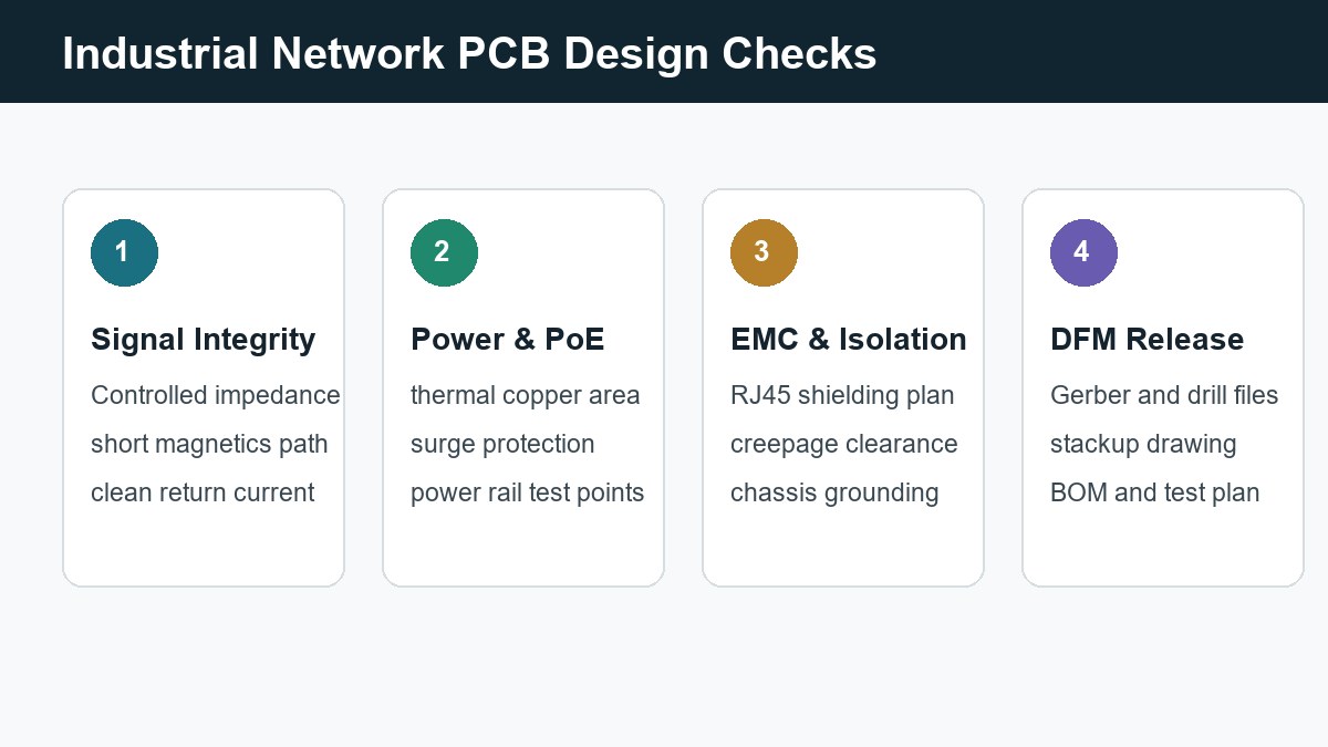
The most useful pre-release checks are signal integrity, PoE or power design, EMC and isolation, connector reliability, and DFM file readiness.

Industrial network PCB design checks for signal integrity, PoE, EMC isolation, and DFM release
Keep the design review focused on the checks that change manufacturing yield, field reliability, and debug time.

Start with the communication path. Ethernet differential pairs, high-speed sensor buses, and clock lines need controlled routing, short return paths, and careful spacing from switching power sections. If the product uses dense connectors or fast edge rates, a standard board may not be enough. In those cases, HDI PCB or tighter multilayer routing may be part of the design discussion.

Next, review power and thermal behavior. PoE, DC input modules, relays, and motor-control interfaces can push current through small board areas. Trace width, copper weight, thermal vias, fuse position, TVS diode placement, and connector current rating should be checked together. A layout that passes electrical simulation can still fail in production if heat concentrates under one regulator or if field wiring injects surge current into the wrong ground path.

Finally, check how the board will be assembled and inspected. An industrial network PCB often has RJ45 connectors, shield cans, terminal blocks, optocouplers, magnetics, LEDs, and test points. Footprint polarity, component height, solder access, and panelization should be reviewed before prototype order. If the project includes mounted components, plan the PCB assembly support at the same time as bare board fabrication.

How Stackup and Materials Affect Network Reliability

Stackup and material choice affect impedance stability, EMI behavior, thermal movement, and long-term reliability more than many buyers expect.

For many industrial control boards, FR4 is still the correct starting point. The decision is not simply “FR4 or special material.” Engineers should define board thickness, copper weight, layer count, reference planes, dielectric spacing, and operating temperature before asking for a quote. A controlled stackup helps keep Ethernet pairs consistent, gives return current a clean path, and reduces layout guesswork.

When the product must handle higher heat, tighter size, high-density connectors, or higher data rates, the board may need high Tg FR4, multilayer construction, impedance control, heavy copper, or special process review. You can use a standard FR4 printed circuit board for many designs, but do not treat the laminate as a default afterthought. Material choice should follow the electrical, thermal, and mechanical load of the device.

EMC, ESD, and Isolation Checks

Industrial network PCB design should give noise and surge current a controlled path instead of letting it travel through sensitive logic or sensor circuits.

Ethernet, RS-485, CAN, and external sensor ports usually connect to cables that may run near motors, relays, power wiring, or long metal frames. That means the PCB must consider ESD, surge, common-mode noise, shielding, creepage distance, and grounding strategy. Protection components should sit near the connector, not deep inside the board after a long trace path.

For RJ45 Ethernet, the magnetics area, shield connection, chassis reference, and differential routing deserve a dedicated layout review. For isolated inputs or fieldbus connectors, isolation slots and clearance rules must be visible in the fabrication data. For noisy power sections, keep switching loops compact and do not route sensitive communication traces under them unless the stackup and return path are deliberate.

Connector and Mechanical Reliability

Connector reliability is a PCB design issue because the board must survive cable insertion, pull force, enclosure fit, and repeated maintenance.

Industrial network products often fail at practical mechanical points: cracked solder joints under heavy connectors, weak cable strain relief, poor board support near terminal blocks, or connector openings that do not line up with the enclosure. A custom PCB should place mounting holes, keepouts, stiff areas, and connector orientation before the layout becomes crowded.

If the board needs edge connectors, shielded RJ45 jacks, terminal blocks, or unusual cutouts, include mechanical drawings with the quote package. Special board shapes, gold fingers, impedance lines, and nonstandard copper requirements should be reviewed as special PCB items rather than handled as ordinary low-risk details.

Production File Checklist for an Accurate Quote

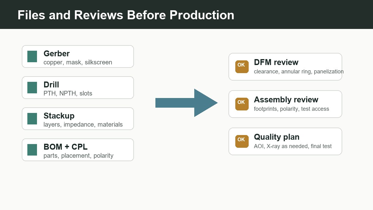
An accurate quote needs fabrication, assembly, mechanical, and testing information, not only a Gerber file.

Files and reviews before production for custom industrial network PCB projects
A complete release package reduces quote assumptions and avoids avoidable engineering questions before production.

For bare PCB fabrication, send Gerber or ODB++ files, NC drill files, board outline, stackup request, copper thickness, surface finish, solder mask color, impedance requirements, special notes, and quantity. For assembly, add the BOM, pick-and-place file, assembly drawing, polarity notes, approved alternates, programming needs, and test requirements.

Do not hide special requirements inside email text only. Put them in the drawing or release note so CAM, procurement, assembly, and quality teams see the same information. If the project is still at prototype stage, prototype PCB assembly can help validate footprints, connector fit, and test points before scaling to a larger build.

Supplier Questions Buyers Should Ask

A supplier for industrial network PCB work should be able to discuss DFM, stackup, assembly, testing, and component risk before production starts.

  • Can you review the Ethernet or high-speed routing stackup before fabrication?
  • Can you confirm minimum annular ring, drill-to-copper clearance, and slot capability?
  • Can you assemble shielded connectors, magnetics, terminal blocks, and mixed SMT/THT parts?
  • How will polarity, connector orientation, and functional test access be checked?
  • Which components in the BOM need alternates or sourcing confirmation?
  • Can you separate bare PCB, assembly, and testing cost drivers in the quote?

BOM risk is often underestimated in custom industrial electronics. Ethernet magnetics, isolated power modules, TVS arrays, terminal blocks, and industrial connectors can have long lead times or multiple acceptable alternates. For that reason, component sourcing should be reviewed before the layout is frozen, especially when footprint-compatible alternates are possible.

Common Mistakes That Delay Industrial Network PCB Projects

Most delays come from unclear files, missing mechanical details, weak test planning, and design choices that are hard to build consistently.

A common mistake is sending only Gerbers when the project also needs controlled impedance, assembly, programming, and functional testing. Another is placing Ethernet connectors and surge protection after the rest of the board is already dense. That often leads to long protection paths, poor grounding, and last-minute compromises around the enclosure.

Buyers also sometimes compare quotes without checking assumptions. One supplier may quote bare boards only, while another includes assembly, component procurement, testing, and fixture work. A lower number is not useful if it excludes the work needed to make the product shippable.

FAQ About Custom PCB Design for Industrial Networks

What makes an industrial network PCB different from a normal PCB?

An industrial network PCB usually connects to cables, machines, sensors, or controllers in electrically noisy environments. It needs stronger attention to EMC, ESD, grounding, connector strength, power stability, test access, and production repeatability than a simple low-speed control board.

Do industrial Ethernet PCBs always need controlled impedance?

Not always, but Ethernet differential pairs and faster interfaces should be reviewed for impedance, stackup, routing length, pair spacing, and return path. If cable length, data rate, EMI risk, or product reliability matters, controlled impedance planning is safer than treating the traces as ordinary signal routes.

What files should I send for a custom industrial network PCB quote?

Send Gerber or ODB++ files, drill files, board outline, stackup, material and copper requirements, BOM, pick-and-place file, assembly drawing, impedance notes, testing requirements, and any enclosure or connector constraints. More complete files reduce quote assumptions.

Can one supplier handle both PCB fabrication and assembly?

Yes, but confirm the supplier can handle the specific connector types, mixed SMT and through-hole parts, BOM sourcing, inspection, and functional test requirements. A one-stop supplier is useful only when the assembly and quality plan match the product risk.

When should component sourcing be reviewed?

Review sourcing before the layout is frozen. Industrial connectors, Ethernet magnetics, isolated modules, TVS arrays, and power components may need footprint-compatible alternates. Early review prevents redesign when a preferred part is unavailable or has an unsuitable lead time.

How can I reduce redesign risk before mass production?

Build a prototype with the real connectors, enclosure constraints, power input, and test method. Check signal behavior, heat, connector fit, assembly yield, and functional test coverage before increasing quantity. Do not rely only on schematic correctness.

Final Checks Before Sending Your Files

Before sending files for quotation or production, check whether the board has a defined stackup, clear connector placement, protected external interfaces, test points, assembly notes, and a realistic BOM.

Custom PCB design for industrial networks works best when electrical, mechanical, assembly, and sourcing requirements are reviewed together. If you are preparing an industrial Ethernet, PoE, sensor gateway, PLC module, or machine-control PCB, send your Gerber files, BOM, stackup request, connector requirements, quantity, and testing needs to sales@bestpcbs.com for engineering review and a practical quote.

You may also like