PCB manufacturing PCB manufacturing
Home > Blog

automotive ECU PCB

ADAS ECU PCB and PCBA Manufacturing for Main Boards
Friday, September 18th, 2026

ADAS ECU hardware must process camera, radar, and vehicle-network data without allowing dense routing, power noise, hidden solder joints, or uncontrolled revisions to weaken the main board. For buyers, the practical challenge is not simply finding a factory that can produce a multilayer PCB. It is making sure the PCB structure, component package plan, assembly process, inspection method, and production files work together.

EBest Circuit (Best Technology) supports PCB fabrication, component sourcing, PCBA, inspection, and customer-defined testing for complex automotive electronics. Send your stackup requirements, Gerber files, BOM, placement data, and test instructions to sales@bestpcbs.com for a manufacturability review of your ADAS computing board.
ADAS ECU
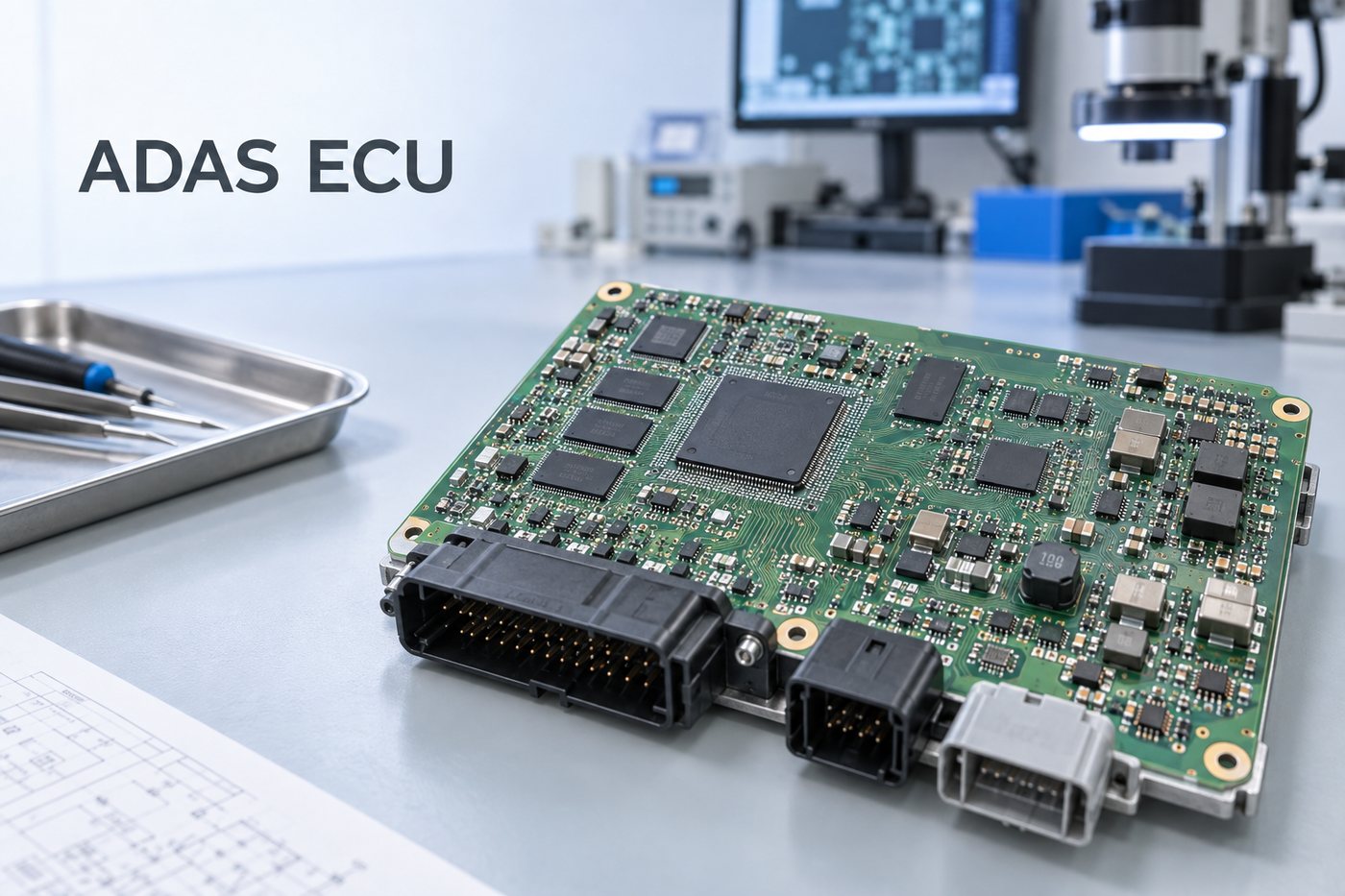
High-density ADAS ECU computing main board prepared for PCB and PCBA manufacturing.

How Is an ADAS ECU Different from Its PCB and PCBA?

An ADAS ECU is the complete electronic control unit used to support advanced driver-assistance functions. Unlike a general electronic control unit board, it is specifically built around the sensing, computing, and communication demands of driver-assistance functions. Depending on the vehicle architecture, it may receive data from cameras, radar sensors, ultrasonic sensors, inertial sensors, or other vehicle controllers. It then runs perception, decision, or sensor-fusion software and exchanges commands or status information with other vehicle systems.

The PCB and PCBA are only parts of that complete controller:

  • ADAS ECU: The complete unit, which may include the PCBA, firmware, application software, connectors, enclosure, shielding, thermal materials, and mechanical mounting.
  • ADAS ECU PCB: The bare printed circuit board before components are assembled.
  • ADAS ECU PCBA or main board: The populated board containing the processor, memory, power circuits, communication interfaces, and supporting components.

This distinction defines the manufacturing responsibility. A PCB and PCBA supplier can review the board for fabrication and assembly, build the bare board, source specified parts, assemble the components, inspect solder joints, and perform agreed tests. Sensor-fusion algorithms, vehicle calibration, functional-safety concepts, cybersecurity, and final vehicle validation normally remain with the customer and its system-development partners.

An ADAS domain controller is a more centralized form of automotive controller. It may consolidate work previously divided among several function-specific ECUs and process more sensor channels on one computing platform. That consolidation can increase processor pin count, memory bandwidth, interface density, power demand, and PCB routing pressure, but it does not change the boundary between the complete controller and the PCBA inside it.

What Components Are Assembled on an ADAS ECU Main Board?

The ADAS ECU architecture on the main board is usually built around a high-performance processor or system-on-chip. The precise component set depends on the number and type of sensor inputs, the software workload, and the vehicle network architecture. A typical board may include:

  • A main SoC, processor, MCU, GPU, or dedicated acceleration device
  • LPDDR4 or LPDDR5 memory close to the processor
  • eMMC, UFS, NOR flash, or other nonvolatile storage
  • PMICs, DC-DC converters, load switches, supervisors, and protection devices
  • MIPI CSI-2, serializer/deserializer, PCIe, Ethernet, CAN or CAN FD, SDIO, SPI, and I2C interfaces
  • Oscillators, clock buffers, filters, ESD protection, and common-mode components
  • Board-to-board, automotive data, power, and service connectors

These parts do not create equal manufacturing difficulty. A large BGA processor and nearby LPDDR devices control fanout and layer planning. Camera and high-speed network channels create impedance and return-path requirements. PMICs and processor rails require low-inductance power delivery. Connectors and protection devices influence component clearance, mechanical support, and EMC behavior.

For the buyer, the useful question is therefore not “How many components are on the board?” It is “Which packages, interfaces, and power rails control the PCB structure and assembly process?” Identifying those controlling features early prevents an apparently complete layout from reaching fabrication with an impractical via structure, incomplete impedance definition, or insufficient inspection access.

When Does an ADAS ECU PCB Require HDI or Additional Layers?

An ADAS ECU PCB does not automatically require HDI. HDI becomes justified when conventional through-hole fanout and the available layer count cannot route the required signals while maintaining reference planes, power distribution, spacing, and manufacturable feature sizes.

The decision is usually driven by five conditions:

  1. BGA pitch and escape density. Fine-pitch processor or memory packages may leave too little room for conventional vias between pads.
  2. Number of high-speed channels. Multiple camera, memory, PCIe, or Ethernet channels need controlled routing space and continuous reference planes.
  3. Board outline and connector locations. A restricted enclosure or fixed connector arrangement can compress routing into a small area.
  4. Power and ground requirements. A high-current processor with several voltage rails may need additional plane area, local copper, and dedicated return paths.
  5. EMC and isolation constraints. Sensitive high-speed circuits, switching power sections, and external interfaces may need physical separation that consumes routing area.

A higher layer count can provide more routing channels and better separation between signal and power structures, but more layers alone do not solve a poor breakout. HDI circuit boards may use laser microvias, blind vias, buried vias, or via-in-pad around fine-pitch BGAs. Each option affects cost, registration tolerance, plating, lamination cycles, inspection, and repairability.

The most economical structure is the least complex stackup that still routes the board with acceptable impedance, return paths, copper distribution, and manufacturing margins. Before release, the PCB manufacturer should review BGA pitch, finished board thickness, via aspect ratio, annular ring, microvia depth, copper weight, material selection, and the proposed lamination sequence.

How Do LPDDR4, MIPI CSI-2, and eMMC Affect the PCB Stackup?

ADAS sensor fusion can place heavy and simultaneous demands on camera inputs, working memory, and stored data. LPDDR4, MIPI CSI-2, and eMMC serve different functions on the board, but they share one basic requirement: the stackup must provide predictable routing layers and uninterrupted reference paths before detailed routing is finalized.

LPDDR4 connects the processor to working memory through a wide, timing-sensitive bus. Memory placement, breakout geometry, reference-plane continuity, via count, and routing length must be planned as one system. Manufacturing cannot correct a topology or timing problem after the Gerber files are released, but the fabricator can verify that the selected trace widths, spacings, dielectric thicknesses, and via structures can be produced consistently.

MIPI CSI-2 commonly carries camera data into the processing platform, sometimes through serializer/deserializer devices rather than a direct camera-to-processor connection. Differential-pair impedance, intra-pair geometry, transitions, stubs, and the return path through connector regions all matter. A nominal impedance value is not sufficient if the fabrication drawing does not identify the controlled structures and their tolerances.

eMMC combines storage, command, and clock connections in a compact package. Although its routing burden may be smaller than a wide LPDDR interface, package breakout, clock quality, power integrity, and proximity to the processor can still affect placement and layer use. SDIO and other synchronous interfaces create similar concerns when clock rate and routing length increase.

The customer should release an impedance table together with the stackup and identify the nets that use each structure. The manufacturer can then calculate manufacturable trace geometries using the selected laminate and copper thickness, return the proposed stackup for approval, and use impedance coupons or agreed test methods to confirm the finished board.

How Should BGA Fanout and Vias Be Planned Around the Processor and Memory?

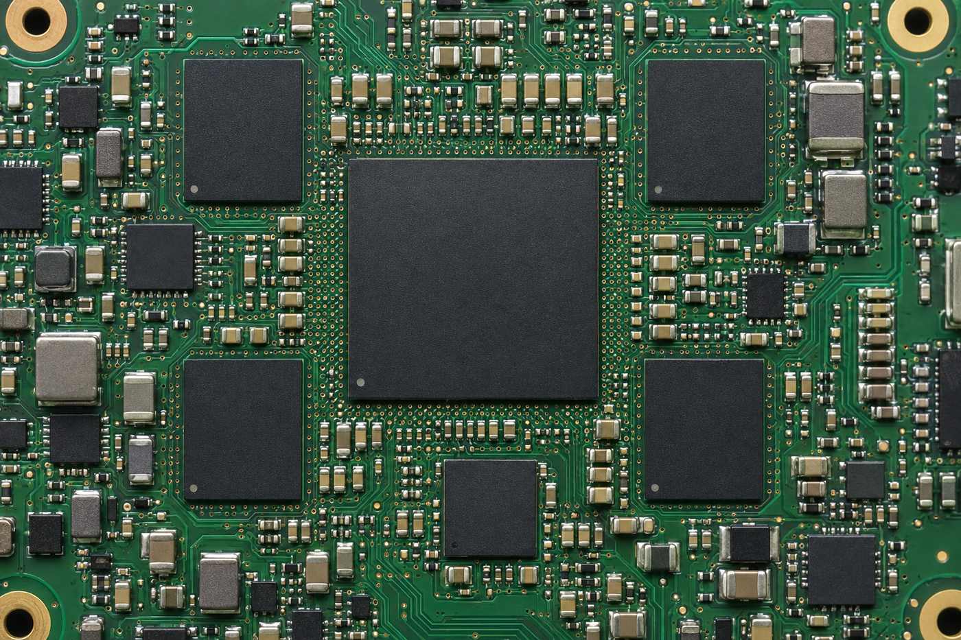
BGA fanout should be planned from the package pitch inward, not selected after routing becomes congested. The first review should compare pad diameter, solder-mask strategy, escape-channel width, finished hole size, annular ring, and the number of I/O rows that must reach internal layers.

For a package that allows through-hole escape, conventional vias may provide the lowest-cost and most repairable solution. As pitch decreases or the number of inner rows increases, through-holes can occupy too much routing area. Laser microvias or via-in-pad structures can open additional escape channels, but they add process controls. Filled and capped via-in-pad features must meet flatness and plating requirements so that solder does not drain into the via or leave an uneven BGA land.

Memory placement also affects fanout. Short processor-to-LPDDR connections may compete with power decoupling, eMMC routing, and processor power escapes. Moving the memory slightly can sometimes remove an HDI bottleneck; in other designs, the enclosure, thermal solution, or timing budget prevents that change. This is why the package drawing, placement, stackup, and routing constraints should be reviewed together.

Fabrication data should clearly identify blind-via spans, buried-via spans, filled vias, capped vias, back drilling if used, and any special acceptance criteria. Ambiguous via notes can cause quotation errors or, more seriously, a board built with a structure different from the designer’s intent.
ADAS ECU
Leadless processor and memory packages create the fanout density that can drive HDI decisions.

How Is an ADAS ECU PCBA Assembled and Inspected?

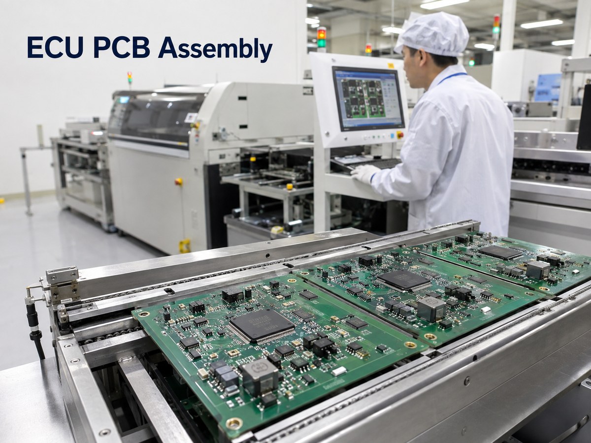
Automotive PCBA assembly for an ADAS ECU requires controls that match the actual package mix. The main processor, memory, storage, PMICs, small passives, bottom-terminated components, and large automotive connectors do not necessarily share the same solder-paste or thermal needs.

Stencil apertures and paste volume should be reviewed in high-density BGA and QFN areas as well as around thermally demanding power components. Component moisture sensitivity, bake requirements, feeder setup, placement accuracy, and the reflow profile must be controlled for the specified parts and board thermal mass. Large copper areas or thick multilayer constructions can change heating behavior across the assembly.

Inspection methods must also match what can be seen:

  • SPI checks solder-paste deposits before components hide the pads.
  • AOI checks visible placement, polarity, component presence, and accessible solder joints.
  • X-ray inspection evaluates hidden BGA, QFN, and via-in-pad solder regions for defects such as excessive voiding, bridging, opens, or abnormal solder distribution.
  • Electrical and functional tests verify the circuits and functions defined by the customer’s test coverage, fixtures, firmware, and acceptance limits.

X-ray is important, but it is not a substitute for process control or electrical testing. A visually acceptable BGA image cannot prove that every high-speed channel, memory connection, or power rail functions correctly. Buyers should therefore define which boards are X-rayed, which joints or regions are reviewed, how results are recorded, and what functional test is required after assembly.

EBest Circuit can coordinate PCB fabrication, specified component sourcing, assembly, AOI, X-ray, and agreed electrical or functional testing. The customer should supply approved firmware, test procedures, fixtures or fixture requirements, and acceptance criteria whenever programming or functional verification is included.
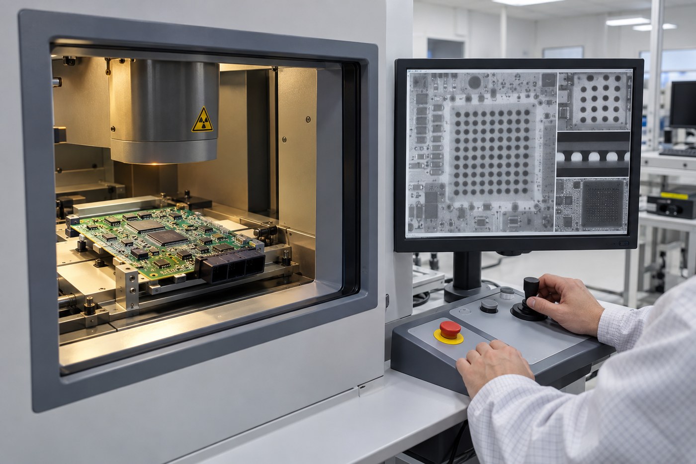
ADAS ECU
X-ray inspection reveals hidden solder-ball patterns beneath BGA packages on an ADAS ECU PCBA.

How Can an ADAS ECU Prototype Be Prepared for Repeatable PCBA Production?

A working prototype is not automatically ready for repeatable production. Repeatability starts when the approved design, materials, process assumptions, and acceptance evidence are converted into a controlled manufacturing package.

Before the next build, the customer and manufacturer should close the following items:

  • Freeze matching revisions of the Gerber or ODB++ data, fabrication drawing, assembly drawing, BOM, centroid file, and approved change records.
  • Confirm the stackup, laminate, copper weight, impedance structures, HDI build, surface finish, and any special via filling or capping.
  • Resolve BOM lifecycle, lead-time, package, polarity, and approved-alternative questions before purchasing.
  • Record stencil decisions, reflow conditions, BGA or QFN X-ray criteria, and any workmanship requirements that differ from the normal process.
  • Define programming files, software versions, fixture ownership, test steps, pass/fail limits, and required test records.
  • Preserve traceability between the board revision, BOM revision, assembly lot, component lots, and test results when the project requires it.

This preparation protects the buyer from three common production problems: building the wrong revision, accepting an unapproved component substitution, and discovering too late that the prototype test depended on an undocumented setup. It also makes quotation and scheduling more accurate because the factory can see which materials, special processes, inspections, and tests belong to the released configuration.

For a new supplier transfer, do not rely only on the previous purchase order. Provide the current controlled package and identify any deviation accepted on earlier builds. A short pre-production review can expose conflicts among the PCB drawing, BOM, placement file, assembly notes, and test instructions before material is committed.

FAQs About ADAS ECU

Is an ADAS domain controller the same as an ADAS ECU?

Not always. An ADAS ECU may perform one defined driver-assistance function, while an ADAS domain controller usually consolidates several functions or sensor channels on a more centralized computing platform. Both contain PCBAs, but a domain controller often creates higher processing, memory, interface, power, and thermal demands.

Does every ADAS ECU PCB need HDI?

No. HDI is appropriate when BGA pitch, fanout density, board size, interface count, or routing constraints cannot be handled efficiently with through-hole vias and a conventional multilayer stackup. The decision should follow a layout and manufacturability review.

How many layers should an ADAS ECU PCB use?

There is no universal number. The layer count depends on BGA escape needs, high-speed signal groups, reference planes, power rails, EMC separation, copper weight, and the available board area. The stackup should be agreed before routing is finalized.

How are hidden BGA solder joints inspected?

X-ray inspection is used to evaluate solder distribution and identify visible evidence of bridging, opens, excessive voiding, or other abnormalities beneath the package. It should be combined with SPI, AOI, process records, and appropriate electrical or functional tests.

What files are needed to quote an ADAS ECU PCB and PCBA?

Provide the Gerber or ODB++ data, fabrication drawing, stackup and impedance requirements, BOM, assembly drawing, centroid file, and any special workmanship, programming, inspection, or test instructions. Include the expected quantity and revision so the quotation reflects the intended build.

If you need a manufacturing review for an ADAS ECU PCB or high-density PCBA, send the controlled project files and expected build quantity to sales@bestpcbs.com. EBest Circuit (Best Technology) can review the fabrication, sourcing, assembly, inspection, and agreed testing scope before production.
You may also like

Electronic Control Unit Board: From Design to Production
Friday, August 21st, 2026

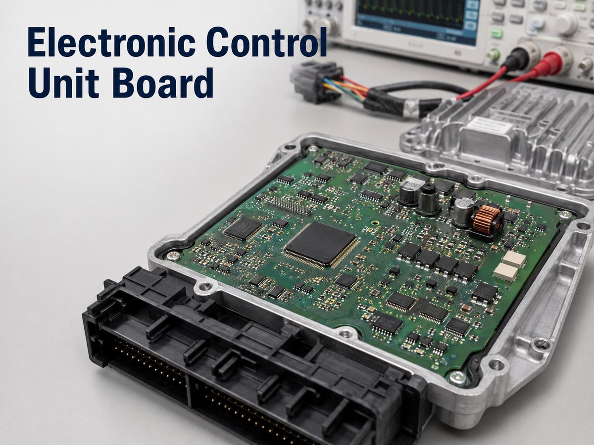
An Electronic Control Unit board is the PCB or PCBA inside an automotive controller. It receives sensor data, runs control software, communicates with other vehicle modules, and drives loads such as motors, valves, relays, and solenoids. Unlike a general controller, an ECU board must remain stable under voltage transients, heat, vibration, moisture, and electromagnetic interference.

EBest Circuit supports ECU PCB design, fabrication, and assembly from engineering review and prototyping to volume production. For a project review, send the Gerber files, BOM, pick-and-place data, drawings, test requirements, quantity, and applicable automotive specifications to sales@bestpcbs.com.

Electronic Control Unit board installed in an automotive ECU enclosure

What Is an Electronic Control Unit Board?

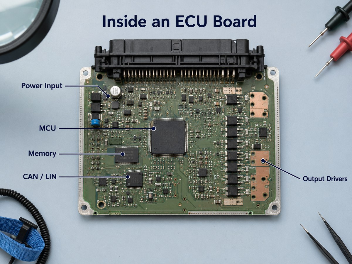
An Electronic Control Unit board provides the electrical foundation of a vehicle control module. The bare PCB contains copper circuits, vias, component pads, and power and ground planes. After assembly, it becomes a PCBA containing processors, memory, communication interfaces, sensor inputs, protection devices, and output drivers.

Several related terms are often confused:

  • ECU: The complete control unit, including the PCBA, software, enclosure, connector, and thermal or sealing components.
  • ECM: An engine control module, which is one type of ECU.
  • ECU board: The bare PCB or assembled PCBA inside the unit.
  • Controller PCB: A broader category covering automotive and non-automotive control boards.

This distinction affects quotation scope. PCB fabrication, component sourcing, assembly, programming, coating, testing, and enclosure integration are separate deliverables unless the quotation states otherwise.

How Does an ECU Board Work?

An ECU board converts vehicle inputs into controlled outputs through several functional stages:

  • The power-input circuit filters the vehicle supply and protects the board from reverse polarity, overvoltage, ESD, and electrical transients.
  • Sensor-interface circuits condition signals from pressure, temperature, position, speed, current, and other sensors.
  • A microcontroller, processor, or system-on-chip compares the input data with programmed control logic.
  • Output drivers operate motors, injectors, pumps, valves, relays, lamps, or solenoids.
  • CAN, LIN, FlexRay, or Automotive Ethernet transceivers exchange data with other vehicle modules.
  • Diagnostic and watchdog circuits detect abnormal conditions and help the system enter a defined safe state.

The balance between these functions depends on the application. A body controller may contain many low- and medium-current outputs, while an ADAS controller places greater emphasis on processing speed, memory bandwidth, controlled impedance, and heat dissipation.

What Components Are Used on an Electronic Control Unit Board?

Most ECU boards contain the same functional blocks, although component count and performance vary.

Main functional components inside an automotive ECU board

Functional block Typical components Main concern
Power input TVS diode, filter, reverse-polarity protection Transients and voltage drop
Power conversion DC-DC converter, LDO, PMIC, inductors Efficiency, ripple, and heat
Processing MCU, MPU, SoC, FPGA Performance, safety, and lifecycle
Memory Flash, EEPROM, RAM Retention and programming
Sensor interface ADC, op-amp, filters, protection arrays Accuracy and noise
Communication CAN, LIN, FlexRay, Ethernet transceivers EMC and signal integrity
Output stage MOSFETs, relays, gate drivers, smart switches Current and junction temperature
Safety monitoring Watchdog and voltage supervisor Fault detection
Timing Crystal, oscillator, clock generator Stability and layout sensitivity

AEC-Q100, AEC-Q101, and AEC-Q200 may apply to ICs, discrete semiconductors, and passive components. These qualifications cover individual components rather than the complete ECU board, so PCB construction and assembly reliability still require separate controls.

Component selection should also consider operating temperature, package reliability, traceability, lifecycle, and approved alternatives. An electrically suitable component can still create production risk if it has limited availability or an unsuitable package.

Which Types of ECU Boards Are Used in Vehicles?

Different vehicle functions place different demands on the PCB.

  • Engine and transmission controllers: Accurate sensor measurement, fast processing, transient protection, and high-current outputs.
  • Body control modules: Multiple connectors and load drivers for lighting, doors, windows, seats, and comfort functions.
  • Chassis controllers: Fault detection and safety-related control for braking, steering, and suspension.
  • ADAS controllers: HDI routing, high-speed memory, controlled impedance, dense processors, and advanced cooling.
  • Battery management systems: Precise voltage measurement, isolation, creepage, clearance, and communication reliability.
  • Gateways and telematics units: Multiple vehicle networks, high-speed interfaces, security devices, and sometimes RF circuits.
  • Motor and inverter controllers: Strong immunity to high-current switching noise and high dv/dt environments.

An interior comfort controller does not need the same laminate, coating, thermal design, or validation plan as an engine-bay or battery-system controller. The mounting location, electrical load, and consequence of failure should guide the specification.

Which PCB Materials and Stackups Suit ECU Boards?

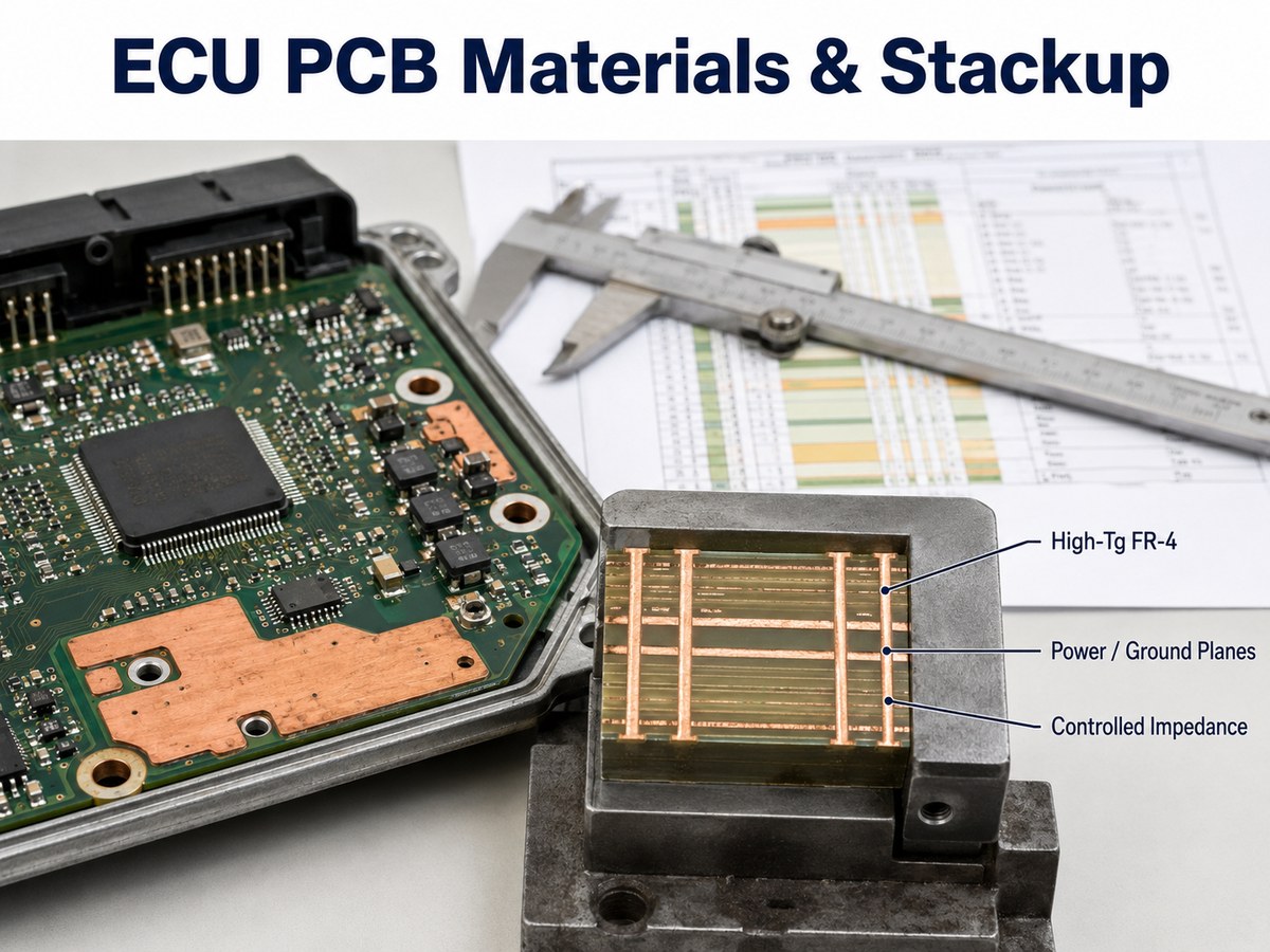
High-Tg FR-4 is commonly used because it supports multilayer construction and established automotive manufacturing processes. However, Tg alone does not determine suitability. The material review should also cover z-axis expansion, CAF resistance, moisture performance, copper adhesion, thermal decomposition, and compatibility with repeated assembly cycles.

Automotive ECU PCB materials and multilayer stackup cross-section

Requirement Suitable PCB construction
Standard body-control functions Multilayer high-Tg FR-4
Fine-pitch processors and memory HDI with microvias
High-current outputs Heavy copper or copper inlay
Automotive Ethernet Controlled-impedance multilayer PCB
RF or radar circuits High-frequency or hybrid laminate
Concentrated power-device heat Thermal vias, copper coins, or enclosure conduction

The approved stackup should define:

  • laminate grade;
  • core and prepreg thicknesses;
  • copper weight on each layer;
  • signal and reference-plane relationships;
  • controlled-impedance requirements;
  • via types and lamination cycles;
  • finished board thickness and tolerance.

Leaving these decisions open until production can change impedance, thermal performance, mechanical stability, and manufacturing yield.

How Should Power and Ground Be Designed on an ECU Board?

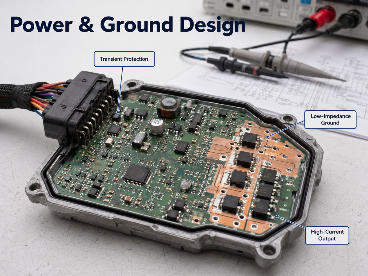
The power input must be designed for the vehicle supply rather than a stable bench source. Applicable transient conditions depend on the vehicle platform, voltage architecture, wiring harness, mounting location, and customer specification. Reverse polarity, cranking, overvoltage, and inductive-load disturbances should be translated into clear protection requirements before the schematic is released.

Automotive ECU PCB power input, grounding and high-current output layout

A typical power architecture includes:

  • input-current and reverse-polarity protection;
  • transient suppression and conducted-noise filtering;
  • regulated power rails and local decoupling;
  • controlled reset and power sequencing;
  • undervoltage and overvoltage monitoring;
  • clamping or freewheeling paths for inductive loads.

High-current returns should not share narrow copper paths with sensor grounds. However, splitting ground planes without analysing return currents can also increase noise and EMI. Power, digital, analogue, chassis, and load-return regions should therefore be connected through deliberate, low-impedance paths.

Copper sizing must account for current, pulse duration, voltage drop, temperature rise, vias, connectors, shunts, and neck-down areas. Widening one section of a trace does not solve a bottleneck elsewhere in the current path.

How Should Signal Integrity and EMC Be Controlled?

An ECU operates near motors, relays, switching converters, ignition circuits, wireless transmitters, and long wiring harnesses. EMC control must therefore begin at the connector and continue through placement, filtering, routing, grounding, shielding, and enclosure design.

Practical layout controls include:

  • place transient protection and filters close to external connectors;
  • route high-speed signals over continuous reference planes;
  • keep switching nodes compact and away from sensor and clock circuits;
  • control the geometry and return path of differential pairs;
  • minimise gate-drive and power-conversion loop areas;
  • place decoupling capacitors close to the relevant power pins;
  • avoid unnecessary stubs on communication buses;
  • provide test points for debugging and pre-compliance measurements.

CAN, LIN, and Automotive Ethernet have different termination, bandwidth, topology, and impedance requirements. They should not be treated as interchangeable two-wire connections.

Emission and immunity limits should be defined in the customer’s validation plan before the PCB layout is finalised. This allows the designer to reserve suitable filtering, shielding, grounding, component spacing, and test access instead of correcting EMC problems after the prototype has been assembled.

How Should Heat Be Managed on an ECU Board?

Thermal design should begin with the real power loss of regulators, processors, MOSFETs, smart switches, shunts, and relays. Average board temperature is not sufficient; each component must remain within its allowable junction temperature under the expected load and ambient conditions.

Common heat-control methods include:

  • wider copper areas around power devices;
  • thermal vias connected to useful internal or opposite-side copper;
  • heavier copper or copper inlays for high-current circuits;
  • exposed-pad packages with controlled solder-paste coverage;
  • thermal interface material between the PCBA and enclosure;
  • component spacing that avoids local hot spots.

Thermal vias provide limited benefit if they connect only to a small isolated copper area. Open vias beneath exposed pads may also draw solder away from the joint. Filled, capped, tented, or offset vias may be preferable depending on the package and assembly process.

Simulation should be followed by measurements on a representative assembly. Thermocouples, infrared imaging, and full-load operating tests help verify the complete heat path through the PCB, interface material, enclosure, and mounting structure.

How Is an Electronic Control Unit Board Manufactured?

An automotive PCB manufacturer should begin with a DFM review covering the stackup, copper balance, drill structure, impedance, panel design, assembly clearances, and test access. Conflicts between the Gerber files, BOM, drawings, and pick-and-place data should be resolved before materials are released.

Automotive ECU PCB assembly on an SMT production line

The main production stages are:

  • bare PCB fabrication and electrical testing;
  • solder-paste printing and SPI;
  • SMT placement and reflow;
  • AOI and X-ray inspection;
  • through-hole or selective soldering;
  • programming and serialisation;
  • ICT, boundary scan, or functional testing;
  • cleaning, conformal coating, or potting;
  • enclosure assembly and final inspection.

Large connectors, relays, transformers, and high-current terminals often require through-hole assembly. BGAs, QFNs, and bottom-terminated power packages generally require X-ray inspection because their solder joints cannot be fully evaluated by AOI.

If conformal coating is specified, the drawing should identify coating type, thickness, coverage, curing method, and keep-out areas. Connectors, programming contacts, grounding features, pressure ports, and selected test points may need to remain uncoated.

Which Tests and Standards Apply to ECU Boards?

No single standard covers the complete ECU board. The applicable combination depends on the vehicle manufacturer, mounting location, safety classification, electrical architecture, and product specification.

For a production-level overview, see our PCB assembly testing services guide.

Standard or control Application
ISO 26262 Functional safety of automotive electrical and electronic systems
ISO 16750 Electrical, mechanical, climatic, and chemical conditions
CISPR 25 Vehicle-component electromagnetic emissions
ISO 11452 Electromagnetic immunity
IPC-6012 Qualification and performance of rigid PCBs
IPC-A-600 Bare-board acceptability
IPC-A-610 Electronic assembly acceptability
IATF 16949 Automotive quality-management processes
AEC-Q100/101/200 Qualification of electronic components
PPAP Production-process and part approval

These documents serve different purposes. ISO 26262 addresses functional safety, while ISO 16750, CISPR 25, and ISO 11452 guide environmental and EMC validation. IPC standards cover PCB and assembly requirements. IATF 16949 applies to the manufacturing quality system, and AEC-Q specifications apply to individual components.

The customer should identify the applicable revisions, test severity, acceptance class, documentation requirements, and any OEM-specific additions before quotation. Without that information, two suppliers may quote very different inspection and validation scopes.

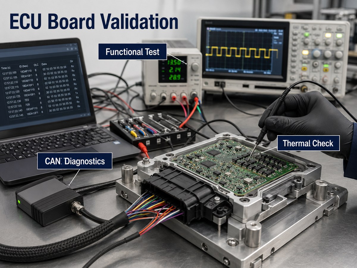
Automotive ECU board functional, thermal and CAN diagnostic validation

What Causes Electronic Control Unit Board Failures?

ECU failures often involve interactions between electrical stress, temperature, vibration, moisture, layout, materials, and manufacturing variation.

Failure symptom Possible cause Investigation or prevention
Intermittent reset Supply drop, ground bounce, cracked joint Review power integrity and solder joints
Communication loss Termination error, connector damage, EMI Test the bus, harness, and transceiver
Burned output stage Overcurrent, transient, inadequate cooling Check the load, clamping, copper, and heat path
Sensor drift Contamination, noise, unstable reference Inspect cleanliness, filtering, and grounding
BGA or QFN open Warpage, voiding, fatigue, board flex Use X-ray, cross-sectioning, or dye-and-pry
Internal PCB short CAF, moisture, contamination Review material, spacing, cleanliness, and humidity
Corrosion Residues, coating gaps, water ingress Improve cleaning, sealing, and coating control

Failure analysis should begin with operating history, fault codes, environmental exposure, and production-lot information. Electrical measurements can then be combined with X-ray, microscopy, cross-sectioning, thermal imaging, or material analysis.

Replacing the visibly damaged component may restore one board, but it does not prove that the underlying design, load, enclosure, or manufacturing issue has been corrected.

What Drives Electronic Control Unit Board Cost?

Cost is influenced by the complete manufacturing and validation package rather than PCB dimensions alone.

The main cost drivers are:

  • layer count and panel utilisation;
  • high-Tg, low-loss, CAF-resistant, or specialised laminates;
  • HDI, microvias, via filling, and sequential lamination;
  • controlled impedance and tighter tolerances;
  • heavy copper, copper inlays, and thermal structures;
  • automotive-qualified components;
  • X-ray, ICT, functional testing, and programming;
  • conformal coating, potting, and enclosure assembly;
  • PPAP documents and customer-specific reports;
  • prototype quantity and component availability.

Useful cost reductions include removing unnecessary HDI structures, improving panel utilisation, standardising material thicknesses, adding practical test access, and approving suitable component alternatives before shortages occur.

The lowest prototype price is not always the lowest production cost. Material substitutions, incomplete testing, poor component traceability, and repeated engineering changes can cost more than the initial saving.

What Should Buyers Check Before Ordering an ECU Board?

First confirm whether the quotation covers a bare PCB, assembled PCBA, programmed controller, or complete boxed unit. The scope should identify included materials, components, testing, documentation, fixtures, and engineering charges.

A complete quotation package should include:

  • Gerber or ODB++ data and drill files;
  • approved stackup and impedance requirements;
  • fabrication and assembly drawings;
  • BOM with manufacturer part numbers;
  • approved component alternatives;
  • pick-and-place data;
  • firmware and programming instructions;
  • test limits and expected outputs;
  • coating, potting, housing, and labelling requirements;
  • prototype and production quantities;
  • required standards, reports, and traceability.

Buyers should also review the supplier’s fabrication capability, SMT and through-hole processes, component controls, engineering response, inspection methods, change management, and automotive quality system.

IATF 16949 certification is relevant, but it should not be the only supplier-selection criterion. Confirm that the certification scope, production location, subcontracted processes, inspection equipment, and documentation system match the actual ECU project.

FAQs About Electronic Control Unit Boards

What does an Electronic Control Unit board do?

An ECU board receives sensor and network data, processes it through a microcontroller or processor, and controls vehicle loads. It also manages power conversion, communication, fault monitoring, diagnostics, and protection against electrical disturbances.

How many layers does an ECU PCB need?

There is no universal layer count. A simple controller may use four or six layers, while an ADAS, gateway, or processor-dense ECU may require additional layers or HDI. The decision should follow routing density, reference-plane needs, power distribution, EMC, and thermal requirements.

What PCB material is commonly used for ECU boards?

High-Tg FR-4 is widely used, but the exact grade depends on temperature, thermal cycling, humidity, CAF resistance, copper structure, and assembly conditions. Heavy-copper, HDI, low-loss, or hybrid constructions should be selected only when the project requirements justify them.

How are ECU boards tested after assembly?

Testing may include SPI, AOI, X-ray, programming verification, ICT, boundary scan, and functional testing. Automotive validation can add thermal cycling, vibration, humidity, electrical-transient, and EMC tests. The customer specification should define the conditions and pass limits.

What information is needed for an ECU board quotation?

For a bare PCB, provide fabrication data, stackup, drawings, material requirements, copper weights, impedance targets, quantities, and acceptance criteria. For PCBA, also provide the BOM, placement data, assembly drawings, programming files, test requirements, and coating or enclosure instructions.

An Electronic Control Unit board must combine protected power inputs, stable signal processing, reliable communication, thermal control, EMC performance, and traceable production. Material and process choices should follow the mounting environment, electrical loads, safety requirements, and validation plan rather than a generic automotive specification.

If you are looking for reliable OEM manufacturing, ODM production, prototype development, volume production, or a custom engineering solution, contact the EBest Circuit engineering team at sales@bestpcbs.com for technical support and a quotation.

You may also like