

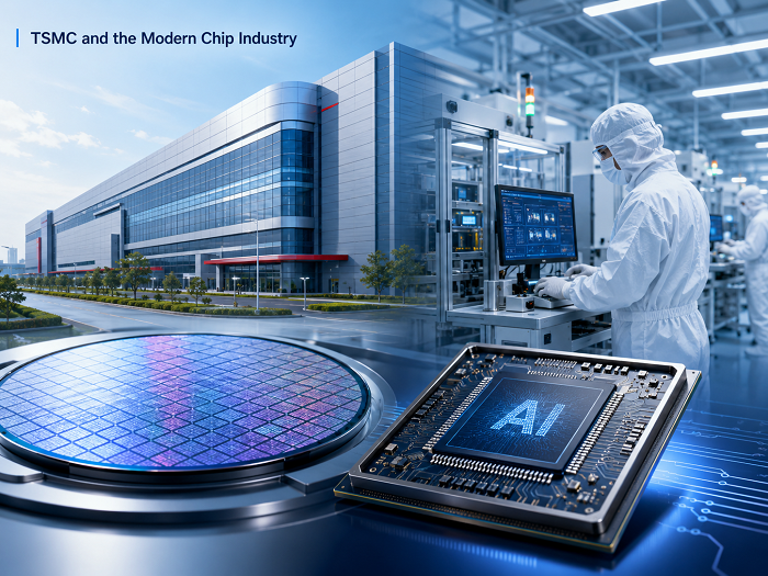
Taiwan Semiconductor Manufacturing Company is one of the most important companies in the global semiconductor supply chain. Many people know it by its shorter name, TSMC. The company does not sell consumer electronics under its own brand. Instead, it manufactures the chips that power smartphones, AI servers, data centers, vehicles, industrial equipment, medical devices, and many other electronic products.
TSMC plays a central role because many chip companies design semiconductors but do not manufacture them in their own wafer fabs. These companies depend on foundries to turn chip designs into real silicon devices. TSMC has become one of the most trusted partners for this work because of its advanced process technology, large manufacturing scale, strong yield control, and growing advanced packaging capability.
What Is Taiwan Semiconductor Manufacturing Company?
Taiwan Semiconductor Manufacturing Company, commonly known as TSMC, is a dedicated semiconductor foundry. It was founded in 1987 and is headquartered in Taiwan. Its main business is manufacturing integrated circuits for customers that design chips but need a highly advanced production partner to fabricate them.
A foundry like TSMC does not usually create the final branded product. For example, a customer may design an AI processor, mobile application processor, automotive controller, networking chip, or power management IC. TSMC then manufactures that chip on silicon wafers using a suitable process technology.
TSMC’s scale is very large. Its official fab capacity page states that the annual capacity of manufacturing facilities managed by TSMC and its subsidiaries exceeded 17 million 12-inch equivalent wafers in 2025.
Is Taiwan Semiconductor Manufacturing Company the Same as TSMC?
Yes. Taiwan Semiconductor Manufacturing Company and TSMC refer to the same company. TSMC is simply the abbreviated name used by engineers, chip designers, investors, customers, suppliers, and industry media.
The full name is often used in formal company profiles, business documents, and introductory explanations. The short name, TSMC, is used more often in daily semiconductor discussions because it is easier to read and instantly recognizable.
What Does TSMC Actually Manufacture?
TSMC manufactures semiconductor wafers and integrated circuits based on customer designs. These chips are used in many markets, including AI computing, mobile devices, automotive electronics, industrial control, communication systems, consumer electronics, and medical equipment.
Its manufacturing portfolio is not limited to one type of chip. TSMC supports advanced logic processes as well as specialty technologies. Its official technology platform includes advanced logic nodes, RF, analog, high-voltage, embedded memory, MEMS, and CMOS image sensor technologies.
In simple terms, TSMC may manufacture chips such as:
- AI accelerators, GPUs, CPUs, networking ASICs
- Application processors, connectivity chips, RF-related ICs
- MCUs, sensors, power control chips, compute processors
- Control ICs, mixed-signal chips, high-voltage ICs
- SoCs, display-related chips, wireless chips
- CMOS image sensors, MEMS-related chips
How Does the Semiconductor Foundry Model Work?
The semiconductor foundry model separates chip design from chip manufacturing. A fabless chip company designs the integrated circuit. The foundry manufactures it.
A typical workflow includes several steps. First, the chip company defines the product function and architecture. Then engineers design the circuit and verify it with design tools. After that, the design must follow the foundry’s process rules so it can be manufactured reliably. Once the design is ready, photomasks are created, wafers are fabricated, and the chips are tested, packaged, and tested again.
TSMC focuses on this manufacturing side, its customers can focus on chip design and product innovation. This division of work has allowed many successful chip companies to grow without owning leading-edge wafer fabs.
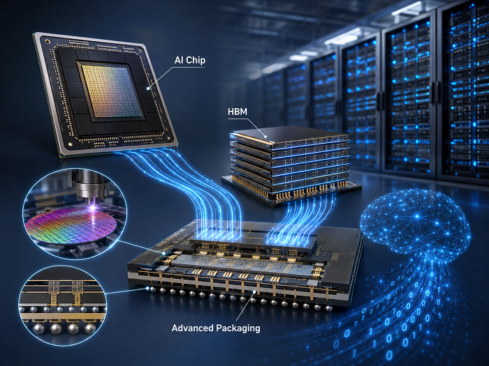
Why Is TSMC Important to AI Chips?
TSMC is important to AI chips because AI needs chips that can process huge amounts of data quickly while using power efficiently. These chips are used in AI servers, data centers, graphics processors, and high-performance computing systems.
Many AI chip companies design their own processors, but they rely on TSMC to manufacture them. TSMC has advanced wafer manufacturing technology, which helps make chips smaller, faster, and more power-efficient. For AI applications, this is critical because powerful chips also generate a lot of heat and consume a large amount of electricity.
TSMC’s CoWoS technology is widely used for high-performance computing and AI-related packages. TSMC describes CoWoS as a platform that integrates chips through wafer-level packaging, silicon interposers, high-density interconnects, and HBM stacks.
For AI hardware, the chip itself is only one part of the performance equation. Wafer process, advanced packaging, IC substrate, PCB layout, power delivery, thermal design, and system assembly all work together.
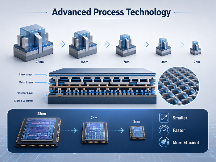
What Makes TSMC’s Advanced Process Technology Different?
TSMC’s advanced process technology is important because it combines transistor scaling, lithography control, materials engineering, design support, yield learning, and high-volume production.
In the semiconductor industry, a process node such as 5nm, 3nm, 2nm, or A14 is not just a size label. It affects transistor density, power consumption, switching speed, leakage current, chip area, and manufacturing complexity. A strong process node must provide useful performance improvement while remaining stable enough for volume production.
For chip customers, advanced process technology can bring several practical benefits:
- Higher transistor density
- Better power efficiency
- Higher performance
- Smaller chip area
- Mature process support
- Better yield learning
However, advanced nodes also increase the pressure on packaging, substrates, PCBs, and assembly. A powerful chip needs strong electrical, thermal, and mechanical support from the rest of the hardware system.
What Is Advanced Packaging and Why Does It Matter?
Advanced packaging is the technology used to connect multiple dies, chiplets, memory stacks, interposers, redistribution layers, and substrates into one high-performance package. It matters because modern chip performance is no longer improved only by making transistors smaller.
For AI, high-performance computing, networking, and advanced mobile devices, data must move quickly between logic, memory, and other functional blocks. If the package cannot support enough bandwidth, the chip cannot reach its full performance.
Advanced packaging helps solve this problem by shortening signal paths, increasing interconnect density, improving power delivery, and supporting multi-die integration. Technologies such as CoWoS, InFO, and SoIC allow different silicon components to work together in one package.
Where Are TSMC’s Major Fabs Located?
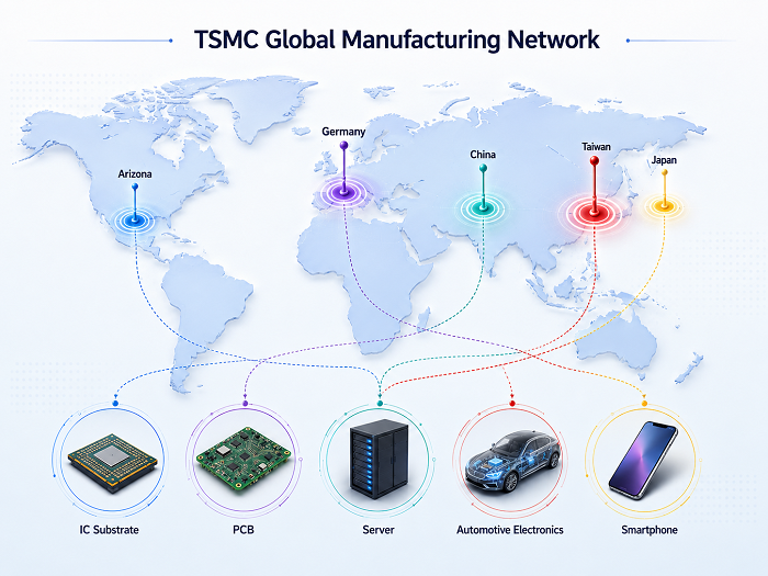
TSMC’s main manufacturing base is in Taiwan, but the company has also expanded in other regions to support global customers.
According to TSMC’s official fab capacity information, the company operates six 12-inch GIGAFAB wafer fabs, four 8-inch wafer fabs, and one 6-inch wafer fab in Taiwan. It also operates 12-inch wafer fabs through TSMC Nanjing and TSMC Arizona, and has a 12-inch wafer fab through Japan Advanced Semiconductor Manufacturing in Kumamoto, Japan.
TSMC’s Arizona project is one of its most visible overseas expansions. TSMC Arizona states that its first fab began high-volume N4 production in the fourth quarter of 2024. The second fab targets N3 volume production in the second half of 2027. The third fab is planned for N2 and A16 process technologies, with volume production targeted by the end of the decade.
FAQs
1. What does Taiwan Semiconductor Manufacturing Company do?
Taiwan Semiconductor Manufacturing Company manufactures semiconductor chips for customers that design integrated circuits. It is best known as a dedicated semiconductor foundry.
2. Is Taiwan Semiconductor Manufacturing Company the same as TSMC?
Yes. TSMC is the short name for Taiwan Semiconductor Manufacturing Company Limited.
3. Does TSMC design chips?
TSMC mainly manufactures chips based on customer designs. Its customers usually handle chip architecture and circuit design.
4. Does TSMC make AI chips?
TSMC manufactures many chips used in AI systems. These chips are usually designed by customers and fabricated by TSMC using advanced process and packaging technologies.
5. Why is TSMC important to AI hardware?
AI hardware needs powerful processors, high-bandwidth memory integration, advanced packaging, and reliable high-volume production. TSMC supports these needs through advanced wafer manufacturing and packaging platforms such as CoWoS.
6. What is CoWoS?
CoWoS stands for Chip on Wafer on Substrate. It is an advanced packaging technology used for high-performance computing, AI processors, and packages that integrate logic chips with high-bandwidth memory.
7. Where are TSMC fabs located?
TSMC’s main fabs are in Taiwan. It also has fabs or major manufacturing projects in the United States, Japan, China, and Europe.
8. Why does TSMC matter to PCB manufacturers?
TSMC matters to PCB manufacturers because advanced chips require better PCB materials, tighter impedance control, stronger thermal design, more precise assembly, and higher reliability.
9. Does TSMC only make leading-edge chips?
No. TSMC manufactures both advanced-node chips and mature-node chips. It also supports specialty technologies such as RF, analog, high-voltage, embedded memory, MEMS, and image sensors.
10. How does TSMC affect IC substrate demand?
Advanced chips often need high-performance IC substrates with fine routing, low warpage, stable dielectric properties, and high-density interconnect capability. This increases demand for advanced substrate manufacturing.
You may also like


Tags: taiwan semiconductor companies, Taiwan Semiconductor Manufacturing, Taiwan Semiconductor Manufacturing Company, TSMC