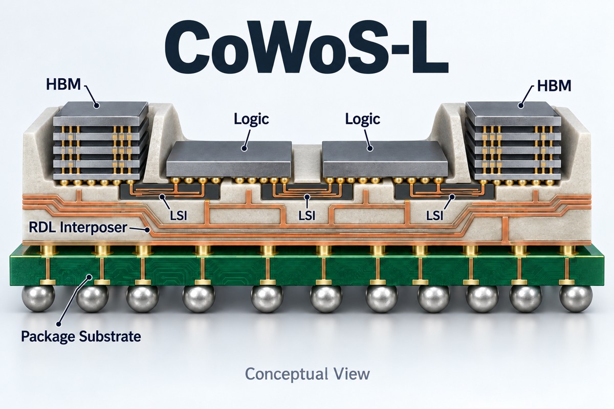
CoWoS-L combines a redistribution-layer (RDL) interposer with local silicon interconnects (LSI). The RDL spans the larger routing platform; embedded silicon bridges provide dense links at selected die interfaces. This division helps integrate more logic and high-bandwidth memory without using one continuous silicon interposer across the full area.
What Is CoWoS-L Packaging?
CoWoS-L packaging is TSMC’s CoWoS architecture that embeds local silicon interconnects within an RDL-based interposer for large multi-die computing packages.
A CoWoS-L cross section contains logic dies and HBM at the top, an interposer incorporating RDL and local silicon beneath them, and a separate package substrate below. RDL means redistribution layer: patterned conductors redistribute connections across the platform. LSI means local silicon interconnect: dense silicon-based routing placed where neighboring die interfaces need it.
Calling this only an “organic interposer” misses the embedded silicon and molded integration structure. It is not silicon-free, and its package substrate is not the system PCB. For the foundry context, see our introduction to TSMC’s manufacturing technologies.
How Do RDL and LSI Work Together in CoWoS-L?
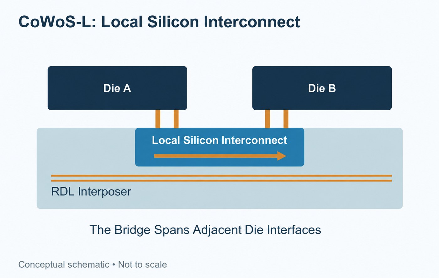
LSI handles dense local die-to-die connections, while RDL distributes connections over the wider interposer footprint.
| Structure | Location | Interconnect role |
| LSI | Selected neighboring die interfaces | High-density local links using fine silicon-based wiring |
| RDL | Across the wider interposer | Broader redistribution and integration with the embedded structures |
| Package substrate | Below the interposer | Connections toward the finished component’s board interface |
TSMC describes CoWoS-L LSI with multiple layers of submicron copper wiring and connections including SoC-to-SoC, SoC-to-chiplet, and SoC-to-HBM. The bridge occupies the region serving those interfaces; it is not simply a small silicon support underneath an arbitrary part of the package.
Consider two logic dies whose high-density interfaces face each other. An LSI region can connect those edges while the wider RDL carries other connections. Rotating one die may move its interface away from the intended landing region, forcing changes to bridge position and routing. Die orientation and LSI placement must therefore be co-designed.
The bridge does not generate bandwidth by itself. Link width, signaling rate, electrical characteristics, and the transmitting and receiving circuits still determine usable throughput.
Why Can CoWoS-L Support Larger Packages?
CoWoS-L extends the interposer footprint through a wider RDL platform while concentrating fine silicon routing at local interfaces, instead of enlarging one continuous silicon interposer everywhere.
TSMC’s public overview identifies a 3.5-reticle CoWoS-L generation that entered production in 2024. This is a dated technology generation, not a permanent maximum. Reticle multiples describe interposer scale relative to an exposure field; they do not specify the component’s outer dimensions, BGA pitch, or HBM count.
- More placement area: the platform can accommodate additional or larger logic and memory components when supported by the package design.
- Localized fine wiring: high-density silicon regions follow the die interfaces rather than covering the entire footprint.
- Separate size limits: interposer area, package substrate outline, and cooling assembly envelope remain different dimensions.
Larger still means more manufacturing coordination. Mold, copper, silicon, and the organic substrate respond differently to temperature. Warpage, interconnect stress, routing yield, and cooling all require qualification. Less full-area silicon does not prove that every CoWoS-L product is cheaper than a CoWoS-S alternative.
How Is a CoWoS-L Package Manufactured?
The CoWoS-L process flow integrates local silicon interconnects into a molded RDL platform, attaches the top dies, and completes the assembly on a package substrate.
- Plan the floorplan: align SoC, chiplet, and HBM interface locations with the required LSI regions and reserve power-routing space.
- Integrate the embedded structures: incorporate the local silicon elements, and applicable embedded passive components, into the reconstituted interposer structure.
- Form the RDL connections: create the redistribution wiring that connects the embedded regions and wider package interfaces.
- Attach the top dies: TSMC describes a chip-last approach in which the interposer platform is prepared before top-chip assembly.
- Complete substrate integration and verification: assemble the package substrate and thermal structure and verify links, power behavior, and reliability.
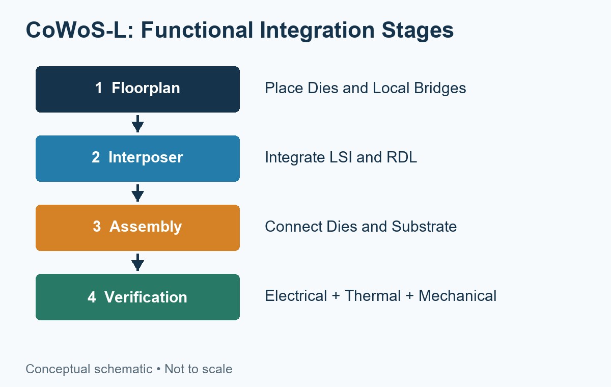
Critical controls include embedded-element position, RDL registration, surface planarity, and joint formation. A displaced bridge or a local height error can compromise the fine die interface even if the overall package outline is correct.
This sequence describes functional stages, not a proprietary process recipe. Exact mold materials, bonding temperatures, tolerances, and inspection acceptance criteria must come from the qualified package process.
How Does CoWoS-L Support Power Delivery?
CoWoS-L supports power delivery through its interconnect network and the integration of stand-alone embedded deep trench capacitors (eDTCs) beneath the SoC.
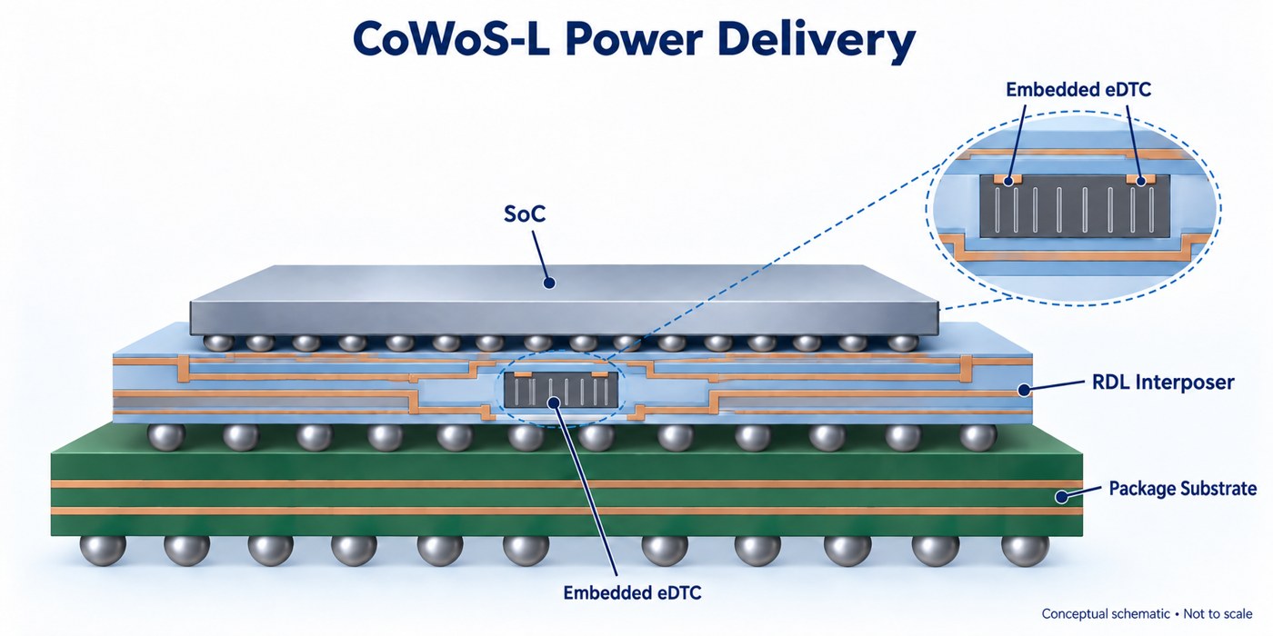
TSMC identifies this eDTC integration in its official CoWoS technology overview. Placing capacitance near the load can shorten the local current loop and reduce the inductive penalty of supplying rapid current changes. The benefit depends on the actual connection geometry, capacitor characteristics, and complete power network.
- Local transient support: nearby capacitance supplies part of a fast current demand before more distant supply paths respond.
- Power-path coordination: package conductors, board planes, capacitors, and voltage regulators must meet the device’s supply limits together.
- Impedance control: capacitance and interconnect inductance can create resonances, so adding capacitance is not automatically an improvement at every frequency.
For an illustrative target, a permitted 30 mV voltage change during a 100 A current step gives Z = ΔV/ΔI = 0.3 mΩ. These are example inputs, not a CoWoS-L rating. A real design needs its own tolerance and frequency-dependent package, board, and regulator models.
Where Is CoWoS-L Packaging Used?
CoWoS-L is used for large AI and HPC packages that need dense local connections among logic dies, chiplets, and HBM on a larger interposer platform.
- Multi-die AI accelerators: local bridges connect the compute interfaces, while the wider floorplan accommodates logic and memory integration.
- HBM-based computing packages: SoC-to-HBM connections combine local routing density with space for the required memory arrangement.
- Chiplet-based HPC designs: dense connections between selected chiplets support integration without making every part of the routing platform silicon.
TSMC’s disclosed SoC-to-SoC, SoC-to-chiplet, and SoC-to-HBM connection forms support these application categories. They are not a claim that every chiplet processor or AI accelerator uses CoWoS-L. Naming a particular product requires a disclosed packaging variant, not an inference from its HBM count or performance.
What PCB Assembly Checks Matter for CoWoS-L Packages?
PCB assembly checks must follow the specific finished component or module’s land pattern, handling limits, reflow instructions, warpage requirements, and thermal-mechanical design.
- Board interface: confirm whether the delivered item is a directly soldered component or a module with its own board/connector interface.
- Land pattern and escape routing: use the released ball map and pad geometry; LSI dimensions do not become PCB trace dimensions.
- Moisture handling and reflow: use the device’s specified storage, exposure, and thermal-profile limits, not a generic “CoWoS-L temperature.”
- Coplanarity and support: review the component’s allowed deformation, board support, heatsink loads, and attachment keep-outs.
- Inspection and testing: agree on accessible joint-inspection methods and electrical or functional tests appropriate to the assembly. Visual inspection alone cannot verify hidden BGA joints.
Our advanced HDI PCB guide covers board-level routing options. At EBest Circuit, we review PCB fabrication and PCBA requirements against the actual design and component documentation—not the interposer’s marketing dimensions. Send your Gerber files, stackup, BOM, quantities, and component assembly specifications to sales@bestpcbs.com. This board-level support is separate from TSMC’s CoWoS-L package manufacturing.
FAQs About CoWoS-L
Does CoWoS-L eliminate silicon?
No. It retains silicon in local interconnect regions. The wider RDL platform changes where silicon is used, not whether silicon is present.
Is LSI another processor?
No. In CoWoS-L, LSI is a local silicon interconnect structure that routes signals between die interfaces; it is not an additional computing die.
Is one LSI bridge enough for every package?
Not necessarily. The number and location of bridges follow the interfaces being connected. Multiple logic dies and HBM stacks can require several local regions.
Does an embedded eDTC replace PCB decoupling?
No. Embedded capacitance supports part of the local supply network. Board capacitors and the voltage regulator must still satisfy the component’s wider power-delivery requirements.
Is 3.5 reticles the maximum CoWoS-L size?
No. It identifies a published production generation rather than a permanent ceiling. Obtain the qualified dimensions and availability for the intended design instead of treating a roadmap target as a released package.