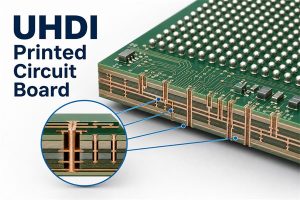
M8 vs M9 CCL is becoming a core material question for AI server PCB design. As 800G networks move toward 1.6T architectures and high-speed SerDes channels move toward 224G-class signaling, M9-class CCL is increasingly discussed as the next step beyond mature M8-class materials.
However, the real engineering question is not whether M9 has a lower nominal Df. The question is whether the complete PCB channel needs enough additional loss margin to justify the higher material cost, tighter supply chain, qualification work, and more demanding multilayer fabrication process.
Key Takeaways
- M8 and M9 are performance-class descriptions, not universal IPC laminate grades. The exact resin, glass fabric, copper foil, and electrical properties depend on the supplier and material part number.
- M8-class CCL is already a mature ultra-low-loss option for many 800G switches, AI servers, and high-speed networking boards.
- M9-class CCL targets even lower transmission loss for next-generation 1.6T networking, longer SerDes channels, and systems with tighter channel-loss budgets.
- The transition from M8 to M9 is not simply a lower-Df resin upgrade. It usually involves the complete material system: resin, glass fabric, copper profile, lamination behavior, and PCB process control.
- 224G-class signaling does not automatically require M9. Channel length, via count, connector loss, copper roughness, routing topology, and insertion-loss budget all matter.
- A 52-layer PCB does not automatically need M9 on every signal layer. Material choice should follow the electrical requirement of each critical channel.
- M8 remains a practical choice when simulation and validation show sufficient insertion-loss, impedance, and reliability margin.
- For RFQs, “M9 material” is not enough. Buyers should specify the exact laminate, Dk/Df conditions, copper foil, glass style, stackup, impedance, insertion-loss target, and qualification requirements.
What Do M8 and M9 Mean in CCL Materials?
M8 and M9 are commonly used as performance-class descriptions for high-speed, low-loss CCL systems, rather than as universal IPC material designations.
Two materials described as M9 can therefore have different:
- Resin chemistries
- Glass fabrics
- Copper foil profiles
- Resin contents
- Dk and Df values
- Test methods
- Processing characteristics
This distinction matters during procurement. A PCB drawing that simply states “M9 material” still leaves too many variables open for accurate stackup design, loss modeling, purchasing, and fabrication.
The correct starting point is the CCL manufacturer and exact material part number, followed by its tested electrical properties, copper construction, glass style, and approved alternatives.
M8 vs M9 CCL: What Are the Main Differences?
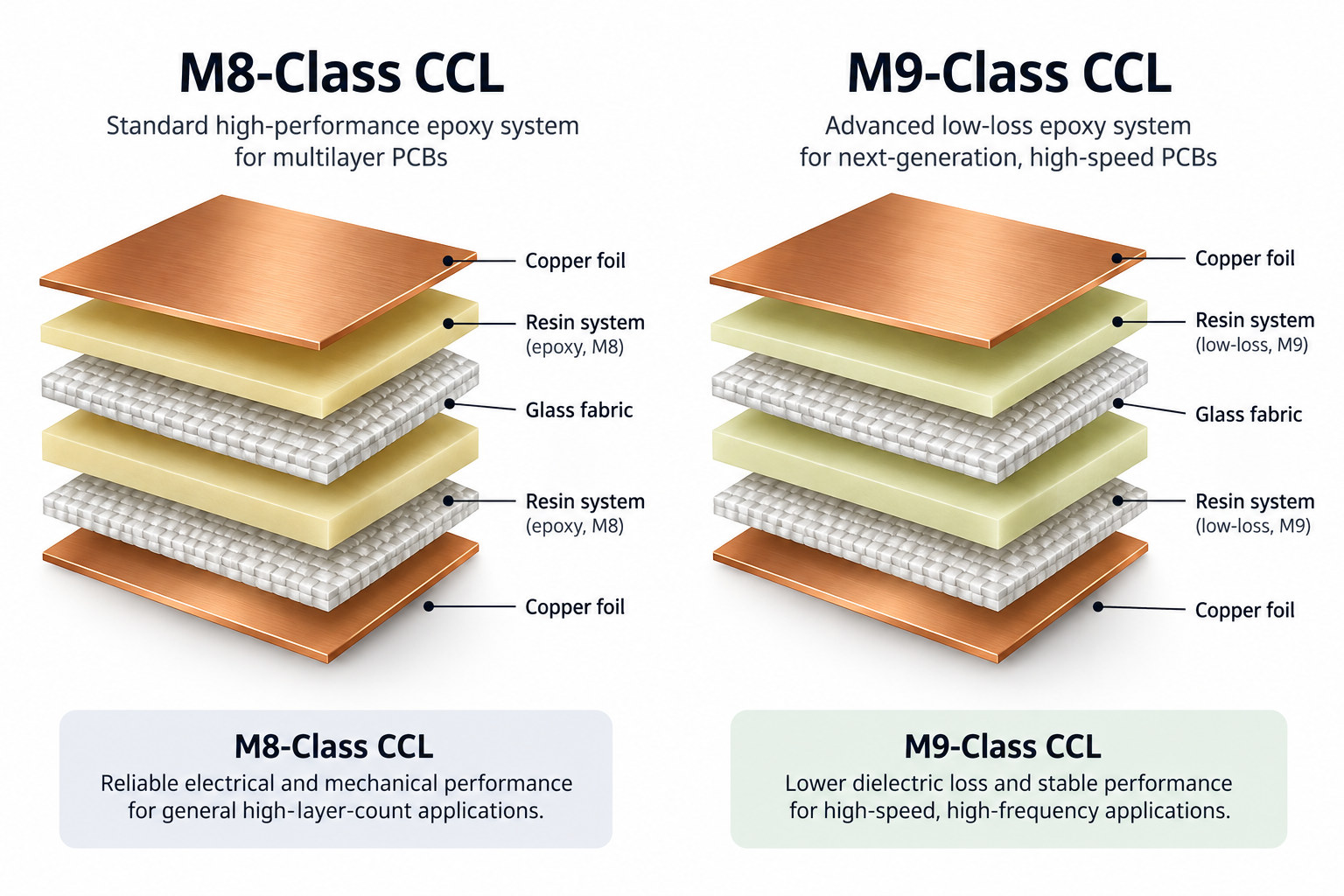
M8-class CCL is already an ultra-low-loss material system for high-speed computing and networking, while M9-class development pushes dielectric loss, conductor loss, dimensional stability, and multilayer process control further for longer and faster channels.
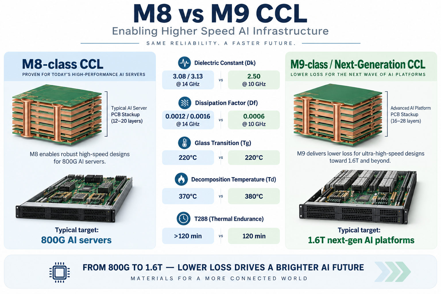
Because M8 and M9 are not universal IPC grades, the most useful comparison combines the general performance direction with published material examples. Panasonic MEGTRON 8 provides a documented M8-class reference, while Doosan DS-7409DYQ illustrates the direction of next-generation material development for 1600G networking and AI accelerators.
| Comparison | M8-Class CCL | M9-Class / Next-Generation CCL |
|---|---|---|
| Typical platform target | 800G switches, current AI servers, high-speed networking | 1.6T switches, next-generation AI accelerators, longer ultra-high-speed channels |
| Published material example | Panasonic MEGTRON 8 R-579Y(U) / R-579Y(N) | Doosan DS-7409DYQ |
| Published application positioning | High-speed networking; supports 800GbE | Super ultra-low loss for 1600G and AI accelerators |
| Dk example | 3.08 / 3.13 @ 14 GHz | 2.50 @ 10 GHz |
| Df example | 0.0012 / 0.0016 @ 14 GHz | 0.0006 @ 10 GHz |
| Tg, DMA | 220°C | 220°C |
| Td, 5% weight loss | 370°C | 380°C |
| T288 | >120 min | 120 min |
| X/Y-axis CTE | 17–20 ppm/°C | 6 ppm/°C |
| Z-axis CTE below Tg, α1 | 50 ppm/°C | 25 ppm/°C |
| Z-axis CTE above Tg, α2 | 270 ppm/°C | 150 ppm/°C |
| Thermal conductivity | Depends on exact construction | 0.4–0.5 W/m·K |
| Water absorption | 0.06% | 0.06% |
| Published copper example | H-VLP3, 1 oz | HVLP3, 1 oz |
| Published peel strength | 0.7 kN/m | 0.5 kgf/cm (~0.49 kN/m) |
| Resin / dielectric direction | Mature ultra-low-loss system | Further optimized extremely low-loss system |
| Glass direction | Low-Dk / ultra-low-Df glass options | Greater emphasis on very-low-loss and dimensionally stable glass construction |
| Copper requirement | Low-profile copper already important | Copper roughness becomes more critical as dielectric loss falls |
| Manufacturing window | Relatively mature for experienced high-speed PCB fabs | Tighter lamination, registration, copper-interface, thickness, and reliability control |
| Supply maturity | More mature and broadly qualified | Fewer qualified material and stackup combinations |
| Cost direction | High | Generally higher |
| Best selection basis | Meets channel loss with sufficient engineering margin | Consider when M8 no longer provides enough channel-loss or qualification margin |
These values show the direction of material development, but they should not be treated as a direct M8-to-M9 percentage comparison. The Panasonic and Doosan data use different frequencies, material constructions, and potentially different measurement conditions. For an actual PCB design, engineers should compare qualified laminate part numbers using the same Dk/Df test method, frequency, glass style, resin content, and copper profile.
Why Are AI Server PCBs Moving from M8 Toward M9?
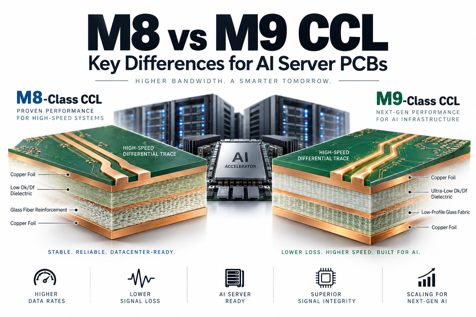
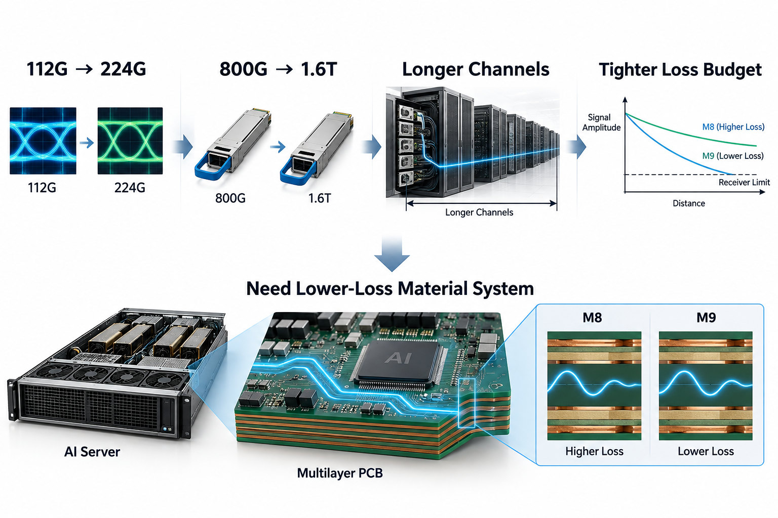
The main reason is that the available channel-loss budget is becoming tighter as data rates increase and signal channels become more difficult.
Several trends are happening at the same time:
- 112G-class channels are moving toward 224G-class signaling.
- 800G network architectures are moving toward 1.6T.
- AI server boards are using more complex multilayer stackups.
- Long SerDes channels may pass through more vias and connectors.
- Phase consistency and impedance control are becoming more demanding.
Higher data rate does not automatically mean M9 is mandatory. A short 224G-class channel with limited via transitions and carefully controlled copper roughness may have a very different loss budget from a long midplane or switch-board channel.
The decision therefore depends on the entire transmission path, including routing length, connector loss, via structure, copper profile, stackup, and any retimers in the architecture.
How Do M8 and M9 Differ in Dk, Df and Transmission Loss?
Df is usually the first specification engineers compare because it directly influences dielectric loss, but Dk and the test conditions behind both values also matter.
Public material data show the general direction clearly. MEGTRON 8 publishes Dk values around 3.08/3.13 and Df values around 0.0012/0.0016 at 14 GHz, while DS-7409DYQ publishes Dk 2.50 and Df 0.0006 at 10 GHz.
Df mainly affects dielectric loss. As trace length and frequency increase, a lower Df can reduce the amount of signal energy lost in the dielectric.
Dk affects impedance, propagation velocity, and trace geometry. A lower Dk can help some high-speed designs, but the lowest nominal Dk is not automatically the best choice. Stability across frequency, temperature, glass construction, and production lots can be just as important.
For real channel modeling, engineers should use material data measured under conditions that match the qualified stackup as closely as possible rather than comparing datasheet numbers from unrelated test methods.
Why Is M9 a Material-System Upgrade Rather Than Just a Lower-Df Resin?
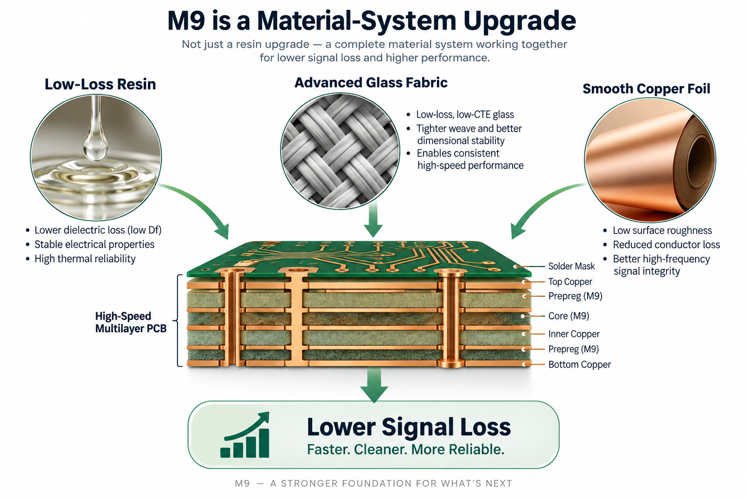
M9-class development is better understood as a system-level material optimization. Reducing resin Df alone does not guarantee sufficiently low PCB channel loss.
Resin System
The resin must reduce dielectric loss while still supporting multilayer PCB manufacturing. Engineers also need to consider resin flow, thermal reliability, adhesion, dimensional behavior, and CAF resistance.
A resin that looks excellent electrically but creates an unstable lamination process does not solve the complete PCB problem.
Glass Fabric
Glass fabric contributes to effective Dk, Df, dimensional stability, and fiber-weave behavior. Advanced low-loss glass constructions can help reduce dielectric loss and limit local variations that contribute to skew and phase mismatch.
Glass style also affects pressed dielectric thickness and manufacturing behavior, so it should be defined at stackup level rather than treated as an invisible material detail.
Copper Foil
Once dielectric loss is reduced, conductor loss becomes a larger part of the total channel budget. Smoother copper becomes increasingly valuable because surface roughness increases conductor loss at high frequency.
This is why many M9-class designs place greater emphasis on very-low-profile copper in addition to lower-loss resin and glass. Our existing HVLP Copper Foil for AI Server PCBs guide explains this conductor-loss mechanism in more detail.
How Much Does Copper Roughness Matter in M8 and M9 PCBs?
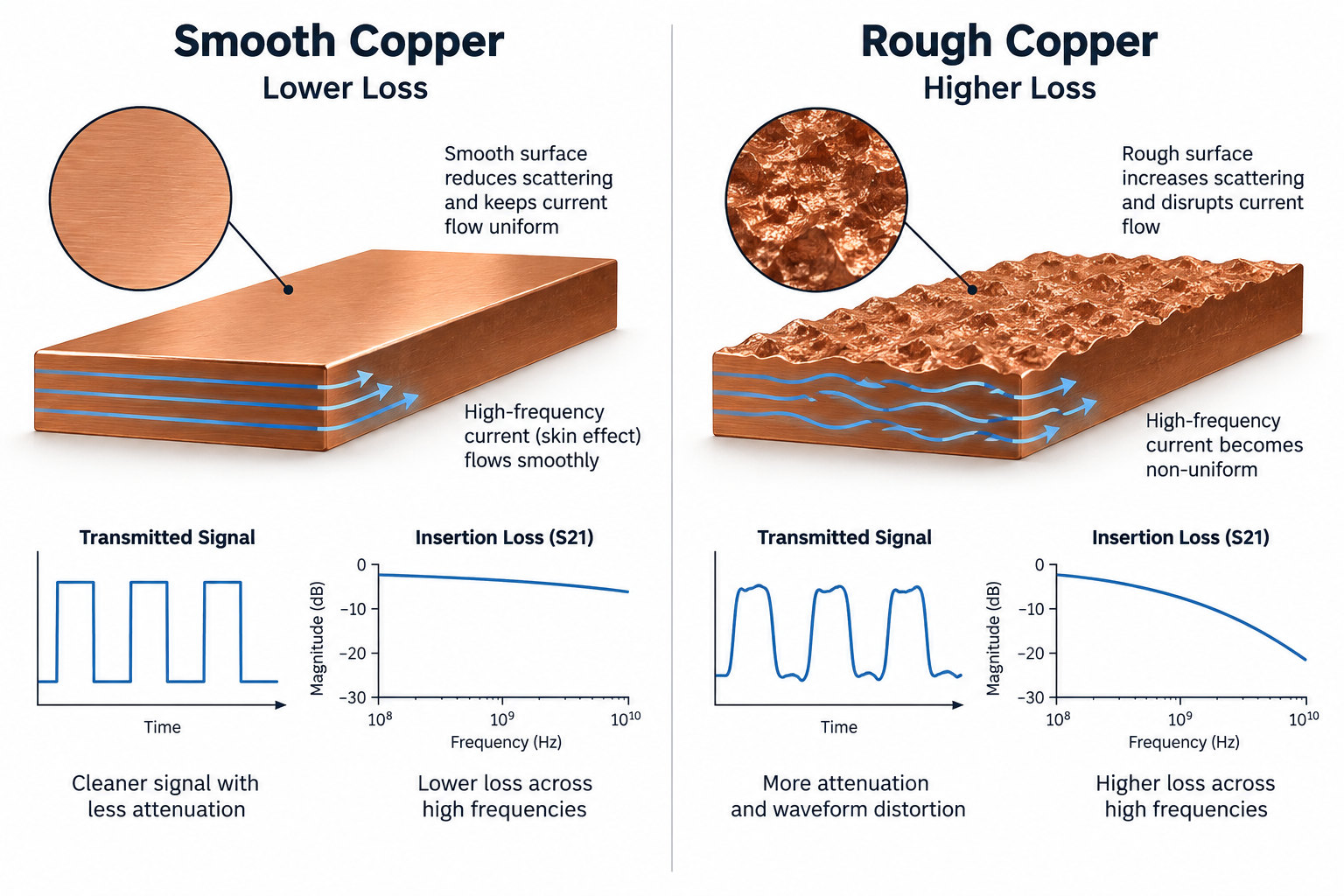
Copper roughness can determine how much of the theoretical low-loss advantage of a laminate remains after PCB fabrication.
At high frequency, current concentrates near the conductor surface because of the skin effect. If that surface is rough, the effective current path becomes more complex, increasing conductor loss.
This means a lower-Df resin can still deliver disappointing channel performance if the signal layer uses an unsuitable copper surface.
For M8 and M9 projects, engineers should evaluate:
- Copper foil type
- Roughness data such as Rz or Rq
- Treatment side
- Foil thickness
- Inner-layer surface treatment
- Final insertion-loss performance
The incoming copper foil grade is only one part of the story. PCB processing can also change the effective copper-dielectric interface, so overly aggressive inner-layer treatment can reduce the benefit of starting with smoother foil.
M9 does not automatically mean HVLP5. Published next-generation low-loss material data can still include HVLP3 copper constructions, which is why the M9 label alone should never be translated into a mandatory copper grade.
When Is M8 CCL Still Enough for an AI Server PCB?
M8 remains a strong choice when the complete channel meets the required electrical targets with sufficient engineering margin.
Typical situations include:
- High-speed channels are relatively short.
- Via transitions are limited.
- Connector loss is manageable.
- Simulation shows acceptable insertion loss.
- Existing M8 materials are already customer-qualified.
- Production experience with the stackup is mature.
- Supply availability and lead time are important.
- Only some signal layers carry the most demanding SerDes channels.
An M8 stackup may therefore remain entirely appropriate even in an advanced AI server platform.
If an M8-based design already meets insertion-loss, impedance, and reliability requirements with sufficient margin, moving to M9 may increase cost without producing a measurable system-level benefit.
This is especially important for boards where only a small portion of the routing approaches the channel-loss limit.
When Should Engineers Consider M9 CCL?
M9 becomes more relevant when the M8 design begins to consume too much of the available channel-loss margin.
Typical triggers include:
- Long 224G-class SerDes channels
- 1.6T switching architectures
- High-loss midplane or backplane routes
- Multiple via transitions
- Very dense high-speed routing
- M8 simulation results close to the insertion-loss limit
- Customer-specified or platform-qualified M9 materials
- Architectures trying to preserve margin without adding additional retimers
The decision should still be based on the actual channel model. A short trace on a high-layer-count PCB may have less need for M9 than a long route on a lower-layer board.
The trigger for M9 should be the channel-loss budget and platform-qualification requirement, not the PCB layer count alone.
Does a 52-Layer or Higher-Layer PCB Automatically Require M9?
No. A 52-layer or higher-layer PCB does not automatically require M9 material on every layer.
A high-layer-count AI server PCB may contain:
- Critical high-speed SerDes signal layers
- Lower-speed control signals
- Clock or management interfaces
- Power planes
- Ground planes
- Auxiliary signal layers
Only some of these layers may be sensitive enough to justify the most aggressive low-loss construction.
In some designs, engineers may consider a hybrid material strategy in which the most demanding signal regions use a higher-performance material system while other layers follow a different qualified construction. Whether this is practical depends on lamination compatibility, reliability, stackup design, and the fabricator’s process capability.
Layer count therefore tells you how difficult the board may be to manufacture, but it does not by itself define the required loss class.
What PCB Manufacturing Challenges Increase with M9-Class CCL?
M9-class materials can narrow the PCB manufacturing window because the electrical advantage must be maintained through lamination, drilling, plating, and inner-layer processing.
Important manufacturing challenges include:
- Multilayer lamination control
- Resin-flow consistency
- Pressed dielectric thickness
- Layer-to-layer registration
- Copper adhesion
- Inner-layer surface treatment
- Mechanical drilling quality
- Plated-through-hole reliability
- Controlled impedance
- Insertion-loss verification
- Material-lot control
Extremely smooth copper needs enough adhesion without introducing excessive surface roughness during inner-layer treatment. This creates a direct trade-off between electrical performance and process robustness.
Advanced glass constructions can also change drilling behavior. Where a qualified M9 construction uses harder low-loss glass, tool wear, hole-wall quality, and drilling parameters may require tighter control.
Before quoting an M9 PCB, the fabricator should review the exact laminate system, stackup, copper foil, glass style, finished thickness, via structure, impedance requirements, and customer qualification rules.
How Should Engineers Choose Between M8 and M9 for a Real PCB Stackup?
The most reliable selection method is to start with the channel requirement and work backward to the material system.
- Define the signaling rate and channel topology. Identify connectors, vias, trace lengths, and any retimers.
- Build the insertion-loss budget. Determine how much loss the PCB portion of the channel can consume.
- Identify the longest and most critical channels. Do not optimize every route based on the worst case unless necessary.
- Simulate an M8 stackup using realistic copper roughness. Nominal Df alone is not enough.
- Compare the remaining margin with an M9 alternative. Evaluate whether the improvement is electrically meaningful.
- Confirm the stackup with the PCB fabricator. Check actual cores, prepregs, glass styles, copper foils, thickness tolerances, and material availability.
The fabricator should be involved before the stackup is frozen. A theoretically ideal dielectric thickness or glass style may not be the construction the factory can source and process consistently.
This step becomes more important as layer count increases because small dielectric-thickness and registration changes can affect impedance, board thickness, and production yield across many lamination interfaces.
What Should Buyers Include in an M8 or M9 PCB RFQ?
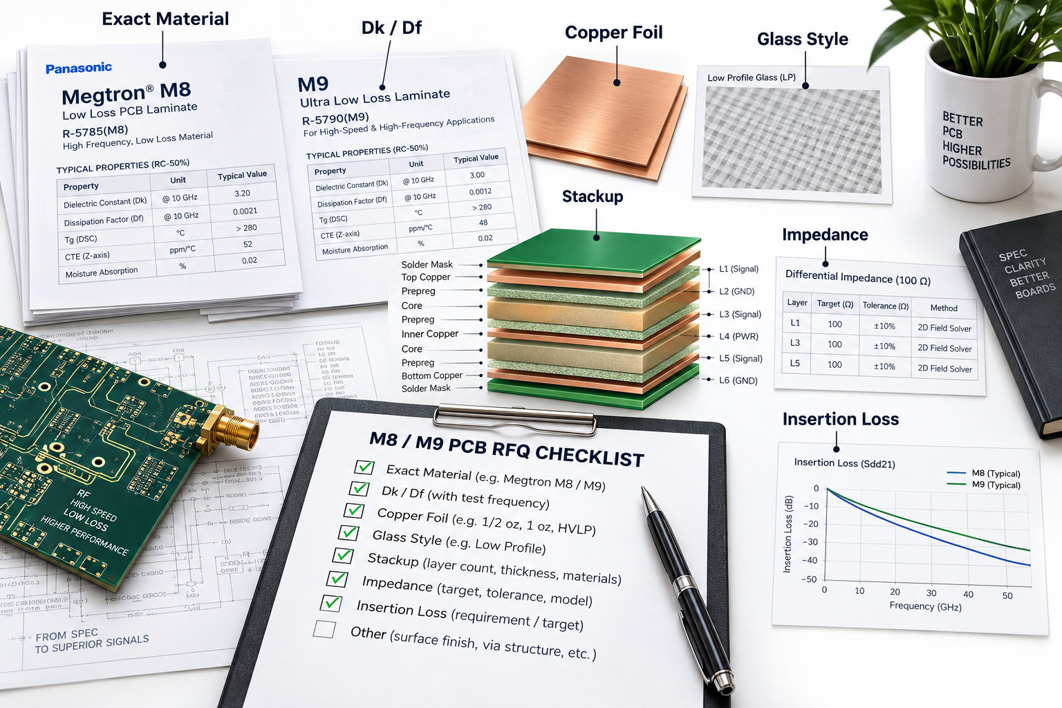
An RFQ should define the material system and electrical target clearly enough that the PCB manufacturer does not have to guess what “M8” or “M9” means.
| RFQ Item | Why It Matters |
|---|---|
| CCL manufacturer and exact part number | Avoids ambiguous M8/M9 descriptions |
| Approved alternative materials | Supports supply continuity |
| Dk/Df and test frequency/method | Makes electrical data comparable |
| Copper foil type and roughness | Controls conductor-loss assumptions |
| Glass style | Affects loss, skew, thickness, and processing |
| Resin content | Influences pressed dielectric behavior |
| Layer count | Defines stackup complexity |
| Finished board thickness | Sets lamination target |
| Impedance table | Defines trace geometry requirements |
| Insertion-loss target | Establishes electrical acceptance criteria |
| Coupon / S-parameter requirement | Defines production verification |
| Customer-approved material list | Controls qualification compliance |
For a high-speed AI server project, the RFQ should also state the via structure and identify the most critical high-speed layers whenever possible.
Writing only “M9 material, 52 layers” is not enough for a reliable technical quotation because two suppliers may interpret that requirement using very different laminate, copper, and glass constructions.
FAQ About M8 and M9 CCL
1. Is M9 CCL always better than M8 CCL?
No. M9 CCL generally targets lower transmission loss, while M8 CCL remains suitable when it meets the channel budget with sufficient margin.
2. Can M8 CCL support 224G-class signals?
Potentially, yes. The result depends on trace length, copper roughness, via count, connectors, routing topology, and the complete insertion-loss budget rather than the M8 label alone.
3. Does every M9 CCL use Q-glass?
No. The search phrase M9 CCL Q glass describes one material direction, but the exact glass fabric must be checked in the qualified laminate construction.
4. Does M9 CCL require HVLP5 copper foil?
No. The required copper profile depends on the qualified material system, channel-loss target, signal layer, and customer approval.
5. Does a 52-layer PCB need M9 on every layer?
No. Material selection should follow the electrical role of each layer and the loss requirements of the critical channels rather than total layer count alone.
6. What information is needed to quote an M9 PCB?
Provide the exact laminate, approved alternatives, stackup, copper foil, glass style, finished thickness, impedance requirements, insertion-loss target, via structure, quantity, and qualification requirements.
Selecting between M8 and M9 requires more than comparing nominal Dk and Df values. Channel length, copper profile, glass construction, stackup, via structure, manufacturing capability, and customer qualification requirements should be evaluated as one system.
For an AI server or high-speed network PCB review, send your Gerber files, stackup, target material, impedance table, insertion-loss requirements, finished board thickness, via structure, and expected quantity to sales@bestpcbs.com.