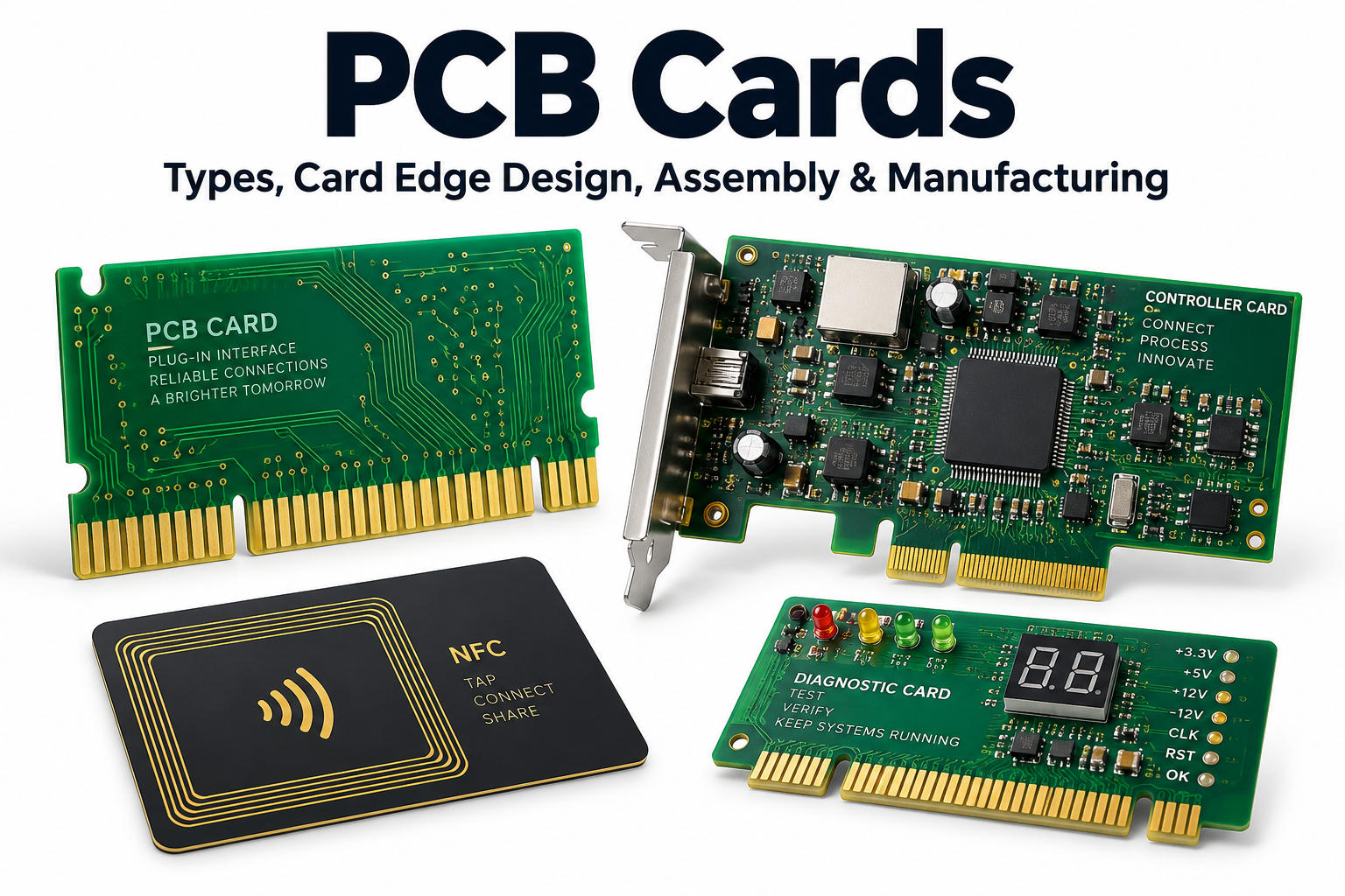
The term PCB cards appears frequently in electronics, but it does not describe one standardized type of printed circuit board. An engineer may use the term for a plug-in communication card, a bare circuit card, an assembled controller board, or even an NFC business card.
For PCB manufacturers, that ambiguity matters. Before fabrication or assembly begins, the actual card function, mechanical interface, component state, stackup, connector requirements, and testing scope must be defined. This guide explains the common meanings of PCB cards and the design and manufacturing details that make card-type PCBs different.
Key Takeaways
- A PCB card is an informal term for a printed circuit board used as an electronic card or module. Depending on context, it may mean a bare PCB, an assembled circuit card, or a plug-in board.
- PCB cards include controller cards, PCIe-style cards, communication cards, card-edge modules, diagnostic cards, NFC cards, and PCB business cards.
PCB card,circuit card,PCBA, andcircuit card assemblyare related terms but should not automatically be treated as identical.- Plug-in PCB cards often use gold fingers along the board edge to mate directly with a socket or card-edge connector.
- Gold-finger design depends on connector pitch, PCB thickness, plating, bevel, mechanical tolerance, insertion cycles, and the manufacturer’s fabrication process.
- A PCB being called a “card” does not define its laminate. Standard FR-4, high-Tg FR-4, and low-loss materials can all be used depending on the application.
- Manufacturing files should clearly specify the board outline, connector interface, gold fingers, stackup, impedance, assembly data, and testing requirements.
What Is a PCB Card?
A PCB card is a printed circuit board used as a functional electronic card or module. Depending on the industry and project documentation, it can refer to either a bare printed circuit board or a populated assembly.
The word “card” is especially common when the board is designed to:
- Plug into another PCB or backplane
- Fit into a defined slot or chassis
- Act as a replaceable functional module
- Use edge contacts as an electrical interface
- Carry a specific control, communication, storage, or test function
Typical examples include network interface cards, industrial I/O cards, motor-control cards, PCIe expansion cards, communication modules, and diagnostic cards.
The important point is that “PCB card” does not automatically tell a manufacturer whether components are assembled. That information must come from the BOM, assembly drawing, pick-and-place data, and purchasing specification.
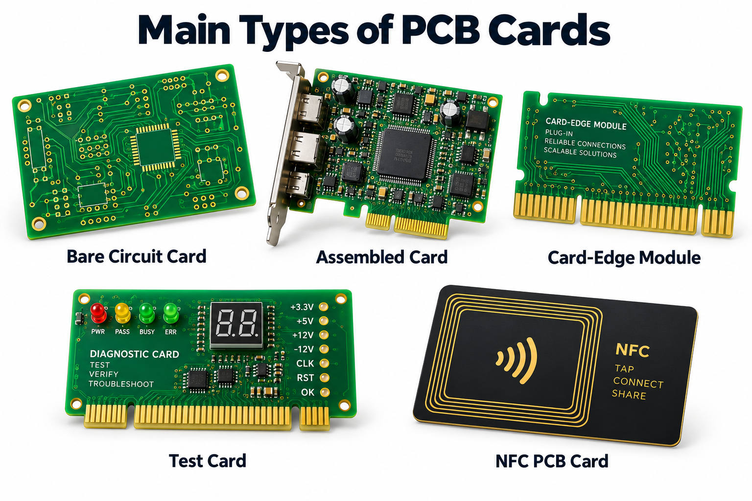
What Are the Main Types of PCB Cards?
PCB cards can be grouped by their mechanical interface, assembly state, and intended function.
| PCB Card Type | Typical Example | Main Characteristic |
|---|---|---|
| Bare circuit card | Unassembled controller PCB | PCB fabrication only |
| Assembled circuit card | Industrial control module | Components already mounted |
| Plug-in PCB card | PCIe or communication card | Inserts into a socket or backplane |
| Card-edge PCB | Memory or interface module | PCB edge acts as connector |
| Test card | Diagnostic or interface board | Used for test and verification |
| NFC PCB card | Smart identification card | PCB antenna and NFC IC |
| PCB business card | Promotional electronic card | PCB used as functional branding item |
The same card can fit more than one category. For example, a communication board can be both an assembled circuit card and a card-edge PCB.
For manufacturing, the functional label is less important than the actual requirements: stackup, board dimensions, copper thickness, connector geometry, surface finish, components, and test criteria.
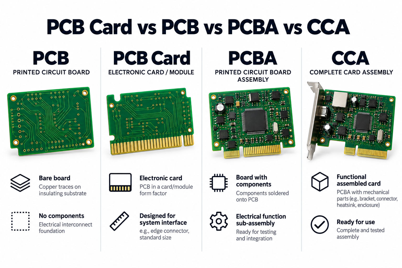
PCB Card vs PCB vs PCBA vs Circuit Card Assembly
These terms overlap, but they describe different things in manufacturing documentation.
| Term | Most Common Meaning |
|---|---|
| PCB | Printed circuit board; may refer to a bare board or the general technology |
| PCB card | Informal term for a board used as an electronic card/module |
| Circuit card | Often another name for a PCB or functional electronic card |
| PCBA | Printed circuit board assembly with components installed |
| CCA | Circuit card assembly; populated functional card |
| Plug-in card | PCB module designed to insert into another system |
| Card-edge PCB | PCB with plated edge contacts that mate directly with a connector |
A bare PCB card has copper circuitry, holes, pads, solder mask, and surface finish but no electronic components. Once components are assembled, it becomes a PCBA or circuit card assembly.
In procurement documents, engineers should therefore avoid relying only on the words “PCB card” or “circuit card.” Specify whether the requirement covers bare-board fabrication, component assembly, programming, functional testing, or a complete tested module.
For a broader terminology comparison, see our guide to Circuit Card vs Circuit Board.
How Does a Plug-In PCB Card Work?
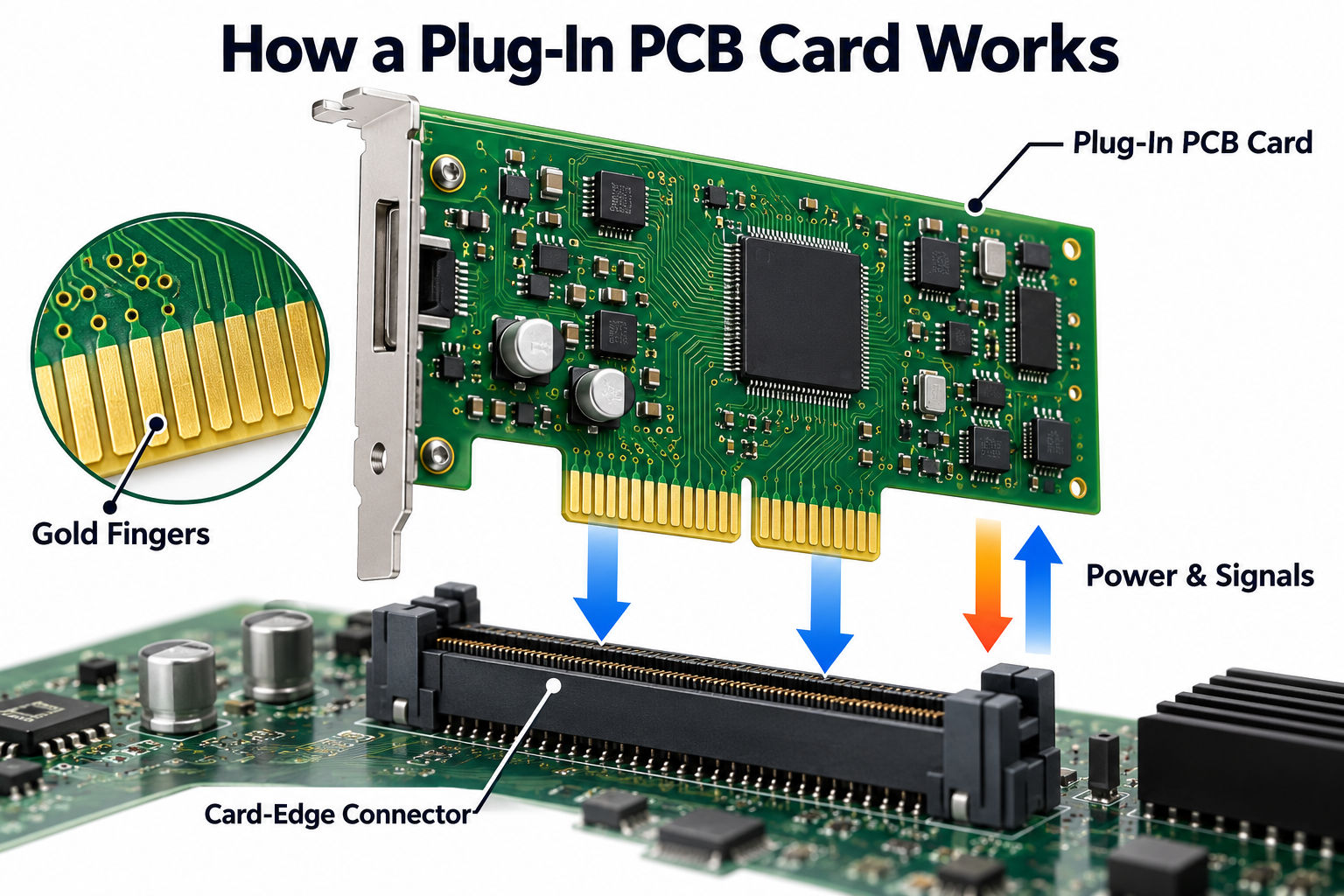
A plug-in PCB card is designed as a removable electronic module that connects electrically and mechanically to another board, backplane, or system socket.
A typical connection path is:
PCB card → edge contacts or connector → motherboard/backplane → system power and signals
The card may carry:
- Processor or FPGA circuitry
- Network interface
- Storage interface
- Industrial I/O
- Motor control
- Power conversion
- Data acquisition
- Test electronics
Unlike a permanently wired PCB, a plug-in card must also satisfy mechanical requirements such as insertion alignment, connector retention, board thickness, chassis position, and repeated mating.
High-speed cards add another layer of complexity because the connector interface becomes part of the signal channel. Differential-pair geometry, breakout routing, via stubs, reference-plane continuity, and connector insertion loss may all affect performance.
This is why plug-in PCB cards should be treated as both an electrical design and a mechanical interface.
What Is a PCB Card-Edge Connector?
A PCB card-edge connector uses plated contacts along the edge of the PCB itself as one half of the connector interface.
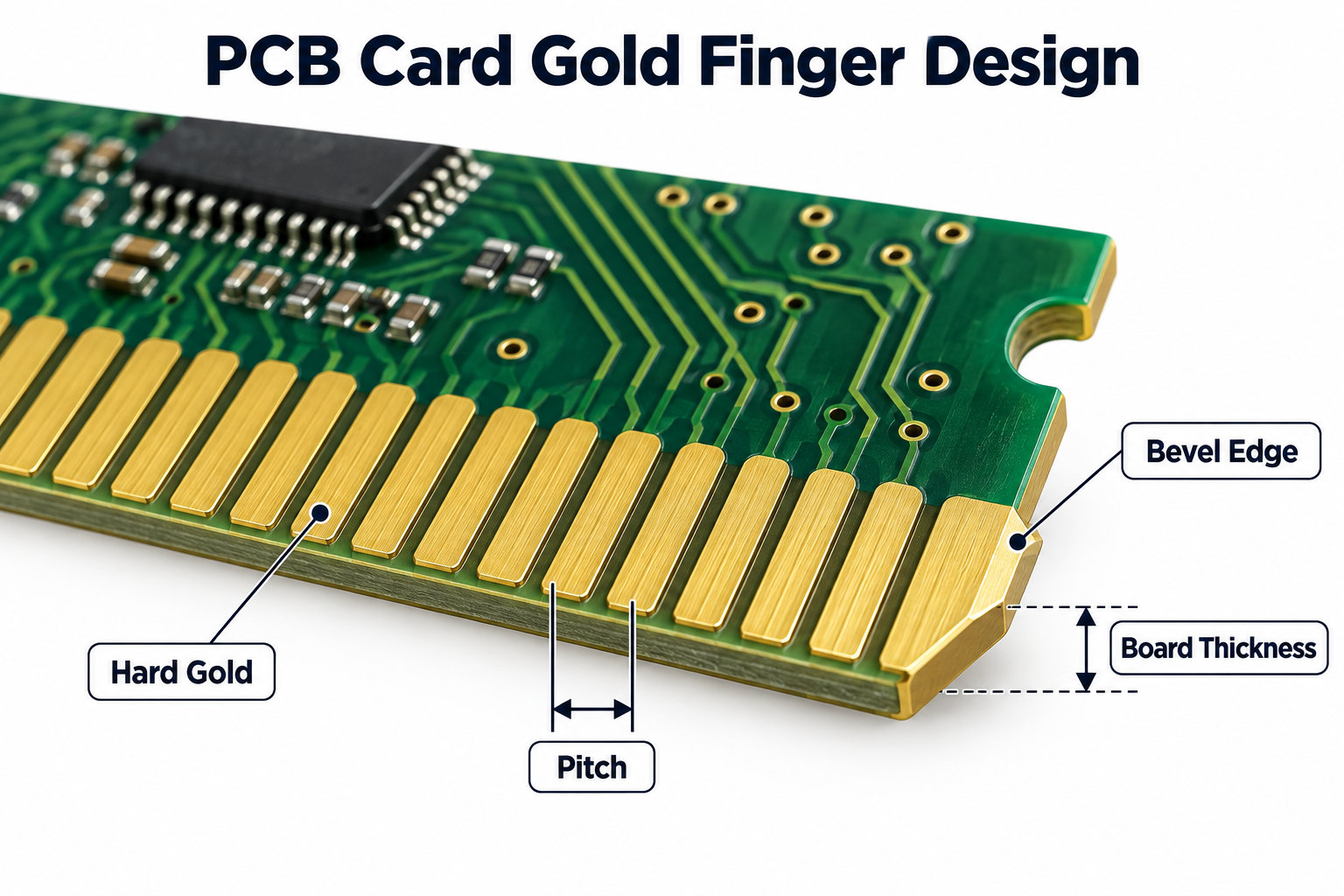
The PCB slides into a matching socket, and spring contacts inside the connector press against the plated pads—commonly called gold fingers.
A card-edge interface may include:
- Single-sided or double-sided contacts
- Different contact pitches
- Power and signal contacts
- Ground contacts
- Staggered contact lengths
- Keying slots
- Beveled insertion edges
- Controlled PCB thickness
This construction removes the need for a separate board-mounted connector on the card itself, which can save space and reduce component count.
However, the PCB edge becomes a precision mechanical feature. Board thickness, routing profile, bevel, plating, pad position, and connector tolerance all need to match the mating connector drawing.
For high-speed interfaces, the card edge also becomes part of the controlled-impedance signal path.
What Design Rules Matter for PCB Card Gold Fingers?
Gold fingers must provide low contact resistance, corrosion resistance, and sufficient wear resistance for the expected mating cycles.
The main design items include:
- Contact pitch
- Finger width and length
- PCB thickness
- Nickel and gold plating requirements
- Solder-mask clearance
- Copper-to-edge spacing
- Bevel angle and depth
- Keying position
- Connector insertion depth
- Required mating-cycle life
Hard gold is commonly preferred for repeated-mating card-edge contacts because it offers better wear resistance than standard solderable surface finishes. The exact gold thickness should follow the connector life, customer specification, and fabrication capability rather than a universal value.
The leading edge may also require a bevel to reduce insertion force and prevent the connector contacts from being damaged. Bevel geometry is determined by the card thickness and mating connector; common designs may use an angled edge in roughly the 30°–45° range, but the connector drawing should control the final specification.
Gold fingers should also be kept free of solder mask, silkscreen, solder paste, surface contamination, and routing damage. For high-current card contacts, power fingers may need wider copper geometry than ordinary signal contacts.
What PCB Materials and Stackups Are Used for Card-Type Boards?
“PCB card” describes the board’s role, not its laminate type. The correct material depends on electrical performance, mechanical strength, thermal environment, and product qualification requirements.
| Application | Common Material Direction |
|---|---|
| General controller card | Standard FR-4 |
| Industrial card | High-Tg FR-4 |
| High-speed communication card | Low-loss / high-speed laminate |
| High-current power card | Heavier copper or thicker copper planes |
| Flexible interface card | FPC |
| Compact 3D module | Rigid-flex PCB |
A simple industrial I/O card may use a conventional multilayer FR-4 construction, while a PCIe or high-speed networking card may require lower Dk/Df materials, controlled impedance, tighter dielectric tolerances, and insertion-loss verification.
Mechanical requirements also matter. Card-edge connectors are often designed for a specific finished board thickness, so the PCB stackup must meet both electrical and connector-fit requirements.
For high-speed cards, stackup decisions should also consider differential impedance, reference-plane continuity, trace-to-plane spacing, copper roughness, glass weave, via structure, and insertion-loss budget.
The material should therefore be selected from the interface and channel requirements rather than from the word “card.”
What Are PCB Test Cards Used For?
A PCB test card is a board designed to support electrical testing, diagnostics, qualification, or connection between a device under test and test equipment.
Depending on the project, the term may describe:
- Diagnostic card
- Interface card
- Fixture interface PCB
- Production test board
- Burn-in card
- Signal breakout card
- Calibration board
For example, a test card can connect production equipment to a DUT through pogo pins, edge connectors, sockets, or cable interfaces.
Some test cards carry active circuits for signal conditioning or measurement, while others mainly route signals between test equipment and the product.
Because PCB test card is not one standardized construction, an RFQ should define the actual application. Useful information includes DUT interface, test voltage/current, signal frequency, connector type, insertion cycle requirements, expected test volume, controlled-impedance requirements, and functional test procedure.
This prevents a manufacturing supplier from treating a demanding high-cycle test card like an ordinary low-volume PCB.
What Are NFC PCB Cards and PCB Business Cards?
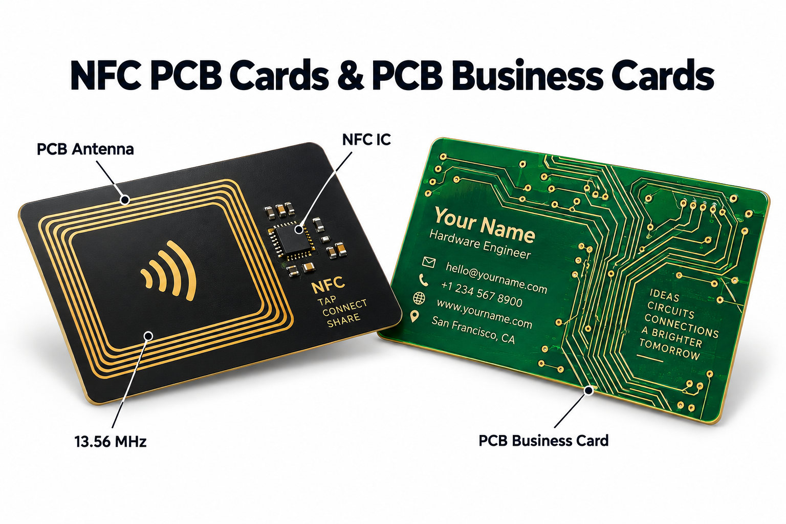
NFC PCB cards are thin printed circuit boards that integrate an NFC antenna, NFC IC, and sometimes LEDs, sensors, QR codes, or other electronics.
Most NFC systems operate at 13.56 MHz. A typical NFC PCB card may include:
- PCB loop antenna
- NFC IC
- Matching or tuning components
- Memory
- LED indicator
- QR code or printed information
PCB business cards often use dimensions close to the ISO ID-1 credit-card format, approximately 85.60 × 53.98 mm, although custom sizes are also common.
A PCB business card does not have to include NFC. It may instead use a QR code, LED circuit, USB interface, small development circuit, measurement reference, functional tool, or decorative copper artwork.
For an NFC version, antenna geometry is critical. Trace width, spacing, number of turns, board thickness, copper environment, nearby ground planes, and metal objects can change antenna inductance and resonance.
The electrical tuning should therefore be verified on the final PCB construction rather than assumed from the CAD geometry alone.
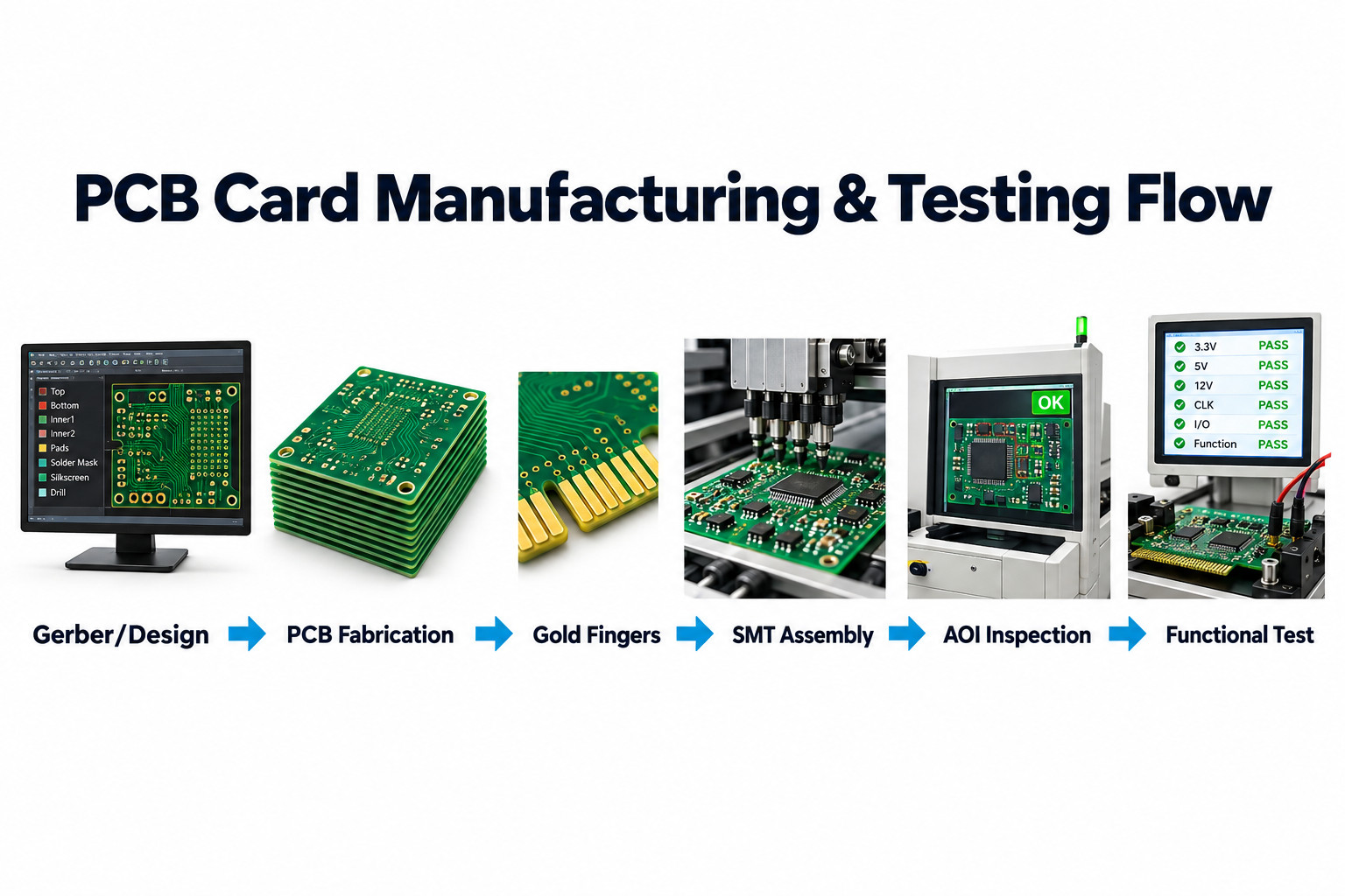
How Are PCB Cards Manufactured and Assembled?
PCB card manufacturing follows the standard PCB production flow, with additional attention to edge geometry and connector interfaces where required.
A typical process is:
Gerber / ODB++ review → PCB fabrication → profile routing → surface finish → gold-finger processing → electrical test → SMT → THT → inspection → functional test
For a card-edge PCB, fabrication may require extra controls for:
- Gold-finger plating
- Edge bevel
- Connector key slots
- Board thickness
- Finger position
- Profile tolerance
- Contact-edge quality
During PCBA, the production flow can include solder paste printing, SPI, SMT placement, reflow soldering, AOI, THT insertion, wave or selective soldering, X-ray where required, programming, and functional testing.
The card connector area should be protected during assembly so that solder, flux, scratches, or handling contamination do not degrade the contact surface. Dimensional inspection is also more important than on a PCB that never mates with a precision slot.
How Should PCB Cards Be Inspected and Tested?
The test plan should match the PCB card’s function rather than automatically applying every available inspection method.
For bare PCB cards, common checks include:
- Electrical continuity/isolation test
- Board dimensions
- Finished thickness
- Hole and slot dimensions
- Gold-finger geometry
- Surface finish
- Controlled impedance where required
For assembled cards, additional inspection can include SPI, AOI, X-ray, ICT, flying-probe test, functional test, and firmware programming.
Card-edge modules may also require contact continuity, connector fit, insertion/removal inspection, finger plating verification, and mechanical gauge checks.
High-speed cards may require TDR, impedance coupon testing, insertion loss, S-parameters, eye-diagram testing, or system-level validation. Not every PCB card needs these tests; the acceptance plan should follow the interface, signal rate, reliability target, and customer specification.
What Files Are Needed to Quote a Custom PCB Card?
A complete RFQ should define both the PCB and the card interface.
| File / Requirement | Purpose |
|---|---|
| Gerber or ODB++ | Defines PCB fabrication data |
| Stackup | Defines layer and dielectric structure |
| Board outline | Controls card dimensions |
| Mechanical drawing | Defines slots, cutouts and tolerances |
| Connector drawing | Confirms mating interface |
| Gold-finger specification | Defines plating and bevel requirements |
| BOM | Defines assembly components |
| Pick-and-place file | Provides SMT coordinates |
| Assembly drawing | Confirms component orientation |
| Impedance table | Defines controlled-impedance requirements |
| Test specification | Defines acceptance and functional testing |
| Quantity | Supports material and process planning |
If a card-edge connector is used, also specify finished PCB thickness, finger pitch, hard-gold requirement, bevel requirement, insertion-cycle requirement, and keying dimensions.
For high-speed PCB cards, include the target stackup, differential impedances, critical interfaces, and any insertion-loss requirement.
The more clearly the interface is defined, the less risk there is that a board can pass electrical fabrication checks but fail to fit or function correctly in the final system.
FAQ About PCB Cards
1. What is a PCB card?
The search query what is PCB card usually refers to a printed circuit board used as a functional electronic card or module. It may be bare, assembled, or designed as a plug-in module.
2. Is a PCB card the same as a circuit card?
Often, but not always. Both terms can describe a printed circuit board, while the exact meaning depends on the industry and project documentation.
3. Is a PCB card the same as a PCBA?
Not necessarily. A PCBA specifically contains assembled components, while “PCB card” can also refer to a bare card-type PCB.
4. Why do PCB cards use gold fingers?
Gold fingers provide durable, corrosion-resistant electrical contacts between the PCB card and a card-edge connector.
5. Can a PCB card include NFC?
Yes. An NFC PCB card can integrate a 13.56 MHz antenna and NFC IC, along with memory, LEDs, or other functions.
6. What should I send a PCB manufacturer for a custom card quote?
Provide Gerber or ODB++, stackup, mechanical drawing, connector and gold-finger specifications, BOM, pick-and-place data, assembly drawing, impedance requirements, test requirements, and order quantity.
PCB cards range from simple controller boards to high-speed plug-in modules, so the word “card” alone is not enough to define a manufacturing requirement. Mechanical interface, assembly scope, connector geometry, stackup, surface finish, and test criteria should be specified together.
For a custom PCB card or circuit card assembly project, send your Gerber files, stackup, mechanical drawings, BOM, pick-and-place files, gold-finger requirements, and test specifications to sales@bestpcbs.com for DFM and manufacturing review.