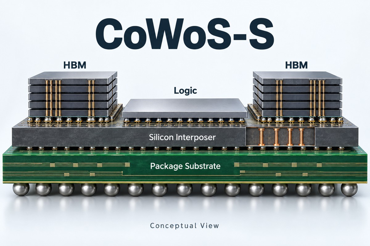
CoWoS-S packaging places logic dies and high-bandwidth memory (HBM) side by side on a silicon interposer. Fine metal wiring connects the dies across that interposer, while through-silicon vias connect it vertically to a separate package substrate. This arrangement supplies the dense, short memory connections needed by AI accelerators and high-performance computing systems.
What Is CoWoS-S Packaging?
CoWoS-S is TSMC’s silicon-interposer version of Chip-on-Wafer-on-Substrate packaging: the “S” identifies the silicon interposer that carries the die-to-die wiring.
Within the CoWoS semiconductor packaging family, its distinguishing feature is a continuous silicon interposer beneath the top dies. The logic and HBM are separate components connected on this shared routing platform, rather than one monolithic chip. HBM itself contains vertically stacked memory dies, but the side-by-side arrangement of logic and memory on the interposer is commonly described as 2.5D integration.
TSMC develops the package technology; the system board sits at a different manufacturing level. Our introduction to TSMC’s manufacturing technologies explains that broader context.
What Is Inside a CoWoS-S Package?
A CoWoS-S package contains logic dies and HBM above a silicon interposer, fine die-attachment connections at their interfaces, and a package substrate beneath the interposer.
| Part | Position | Function |
| Logic die | Above the interposer | Processes data and controls memory access |
| HBM stack | Beside the logic die | Provides wide-interface, high-bandwidth memory |
| Microbumps | Between top dies and interposer | Connect die pads to interposer wiring |
| Silicon interposer | Below logic and HBM | Routes dense connections between dies |
| Through-silicon vias (TSVs) | Through the interposer thickness | Carry connections to its underside |
| Package substrate | Below the interposer | Redistributes connections toward board-facing terminals |
The CoWoS S silicon interposer is primarily an interconnect platform, not an additional processor. It can also incorporate passive functions such as integrated capacitance. The silicon interposer, organic package substrate, and system PCB are therefore three distinct structures—not interchangeable names for the same board.
Underfill and the thermal assembly complete important mechanical and heat-transfer functions. Their materials depend on the qualified package design; a conceptual cross section does not specify an actual lid, thermal-interface material, or assembly thickness.
How Does CoWoS-S Connect Logic Dies and HBM?
Logic-to-HBM signals travel from a die’s pads through microbumps, laterally along the interposer’s metal wiring, and through another set of microbumps into the memory interface.
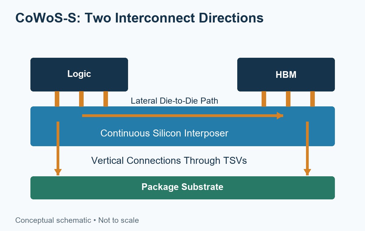
This lateral memory path is different from the vertical path through interposer TSVs toward the package substrate. An HBM data signal does not have to travel down to the system PCB and back up to the neighboring memory stack. Keeping many connections within the package supports a wide memory interface without routing that interface across the board.
- Connection density: fine interposer wiring accommodates many parallel signal connections in a small area.
- Shorter paths: adjacent die placement reduces the distance compared with off-package memory routing, although actual delay and loss depend on the layout.
- Matched interfaces: logic memory controllers, HBM generation, pad maps, and package routing must work together. An interposer alone does not set bandwidth.
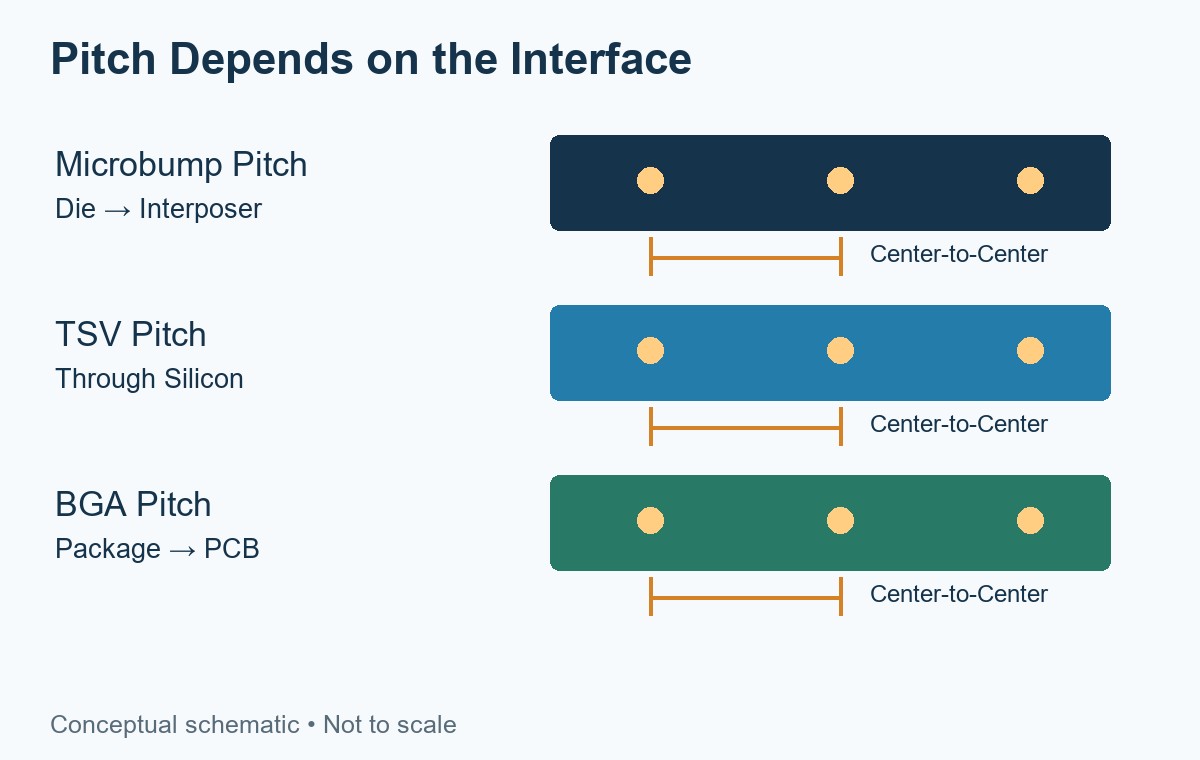
CoWoS S bump pitch refers to center-to-center spacing at a specified bump interface. It must not be confused with TSV pitch, metal line spacing, or board-level BGA pitch. For example, a hypothetical 40 µm pitch with 20 µm-wide pads leaves a nominal 20 µm edge gap; those illustrative dimensions are not a CoWoS-S specification.
How Is a CoWoS-S Package Manufactured?
The CoWoS-S process flow prepares the silicon interposer, attaches the logic and memory dies to it, and integrates the resulting assembly with a package substrate.
- Design the interconnect platform: coordinate die locations, HBM interfaces, routing layers, TSVs, and power connections.
- Fabricate the interposer: form fine metal interconnects and the required through-silicon connections. Large designs may use lithographic stitching across exposure fields.
- Prepare the backside connections: thinning and backside processing provide access to the interposer’s vertical interconnects.
- Attach the top dies: align the logic and HBM interfaces with the interposer connections and form the die joints, with appropriate mechanical reinforcement.
- Complete and verify the package: integrate the package substrate and thermal structure, then check electrical operation and package reliability.
These are public functional stages, not a recipe for TSMC’s proprietary production line. Bonding temperatures, process ordering, tolerances, and inspection limits require the applicable qualified process documentation.
Reliability depends on more than electrical continuity. Silicon, copper, underfill, and substrate materials expand differently during temperature changes. TSMC’s 2013 CoWoS reliability work examined underfill and lid choices, including AlSiC versus copper, in relation to interconnect fatigue. That dated study illustrates why the complete assembly must be qualified; it does not prescribe a lid material for every modern package.
What Limits CoWoS-S Interposer Scaling?
CoWoS-S interposer scaling is constrained by stitched routing, defect exposure, wafer utilization, assembly yield, and mechanical control—not by an absolute one-reticle limit.
TSMC has publicly described reticle stitching to extend silicon interposer area beyond a single exposure field. Its 2021 fifth-generation CoWoS-S publication reported an approximately 2,500 mm² interposer supporting multiple logic dies and eight HBM stacks, with five layers of submicron copper wiring and second-generation integrated capacitors. This is a specific published configuration, not a mandatory HBM count or permanent size ceiling.
- Stitching: interconnects crossing exposure boundaries require controlled pattern alignment and continuity.
- Yield: increasing area exposes more routing and structures to possible defects; the economics also depend on die and assembly yields.
- Mechanical integration: larger assemblies require coordinated substrate, underfill, lid, and cooling design.
- Usable floorplan: logic sizes, HBM placement, power regions, and keep-outs determine how much area is actually available.
Interposer area is not the package outline: the substrate and thermal assembly can extend beyond it. Nor can an area in square millimeters be converted into a package width without knowing the shape.
For larger integration footprints, CoWoS-L uses a wider RDL platform with local silicon interconnects rather than extending one continuous silicon interposer. The TSMC CoWoS overview describes these architecture options; their full comparison belongs in a separate S-versus-L discussion.
Where Is CoWoS-S Packaging Used?
CoWoS-S packaging is used in high-end computing products that need dense connections between processing dies and high-bandwidth memory, including AI acceleration and HPC.
- AI accelerators: memory bandwidth helps feed compute units with model weights and intermediate data. The benefit depends on the workload, not simply the presence of HBM.
- HPC processors and accelerators: simulations and other data-intensive calculations can require substantial bandwidth between compute and memory.
- Multi-die computing designs: a shared interposer provides dense routing between separately fabricated logic and memory components.
TSMC’s 2022 annual report identifies CoWoS-S with high-end HPC and AI and describes HBM3-related qualification. Together with the published eight-HBM fifth-generation example, this provides concrete application context without assuming that every GPU, accelerator, or HBM product uses CoWoS-S. A named chip’s packaging variant still requires its own disclosure.
How Does a CoWoS-S Package Connect to a PCB?
A finished CoWoS-S component connects to the PCB through its package substrate and board-facing terminals, commonly a BGA interface—not through the interposer’s microbumps.
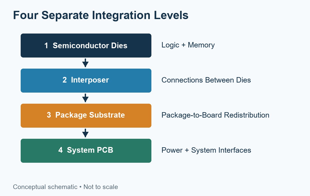
The component’s released land pattern, ball map, power requirements, and assembly guidance determine the board design. The PCB routes external interfaces and supplies power; it does not reproduce the fine logic-to-HBM wiring inside the package.
- Layout: select escape routing and via structures from the actual BGA geometry.
- Power: design planes, regulator connections, and board decoupling for the component’s current and voltage limits.
- Assembly: follow the device-specific handling, reflow, warpage, and inspection requirements.
- Mechanical support: coordinate heatsink attachment, board support, and package keep-outs.
Our guide to advanced HDI PCBs explains board-level routing structures. At EBest Circuit, we support PCB fabrication and PCBA projects around qualified components; we do not claim to manufacture TSMC’s interposers. Send your Gerber files, stackup, BOM, quantities, and package assembly requirements to sales@bestpcbs.com for a board-level review.
FAQs About CoWoS-S
Is CoWoS-S the same as SoIC?
No. CoWoS-S provides interposer-based integration, while SoIC addresses a different level of die stacking and bonding. These technologies can be combined in a larger integration scheme.
Are HBM TSVs and interposer TSVs the same structures?
No. HBM TSVs connect dies within the memory stack; interposer TSVs pass through the separate silicon interposer. They occupy different parts of the package.
Does every CoWoS-S package contain eight HBM stacks?
No. Eight stacks describe one published configuration. The actual count depends on the processor interfaces, memory requirements, floorplan, and qualified package design.
Does reticle stitching mean joining separate pieces of silicon?
No. It joins lithographically patterned regions across exposure fields on the interposer. It does not mean gluing individual silicon tiles together.
Can HBM be replaced like a DIMM?
No. HBM is integrated into the package assembly rather than installed in a board-level memory socket. Replacement is not equivalent to changing a server DIMM.