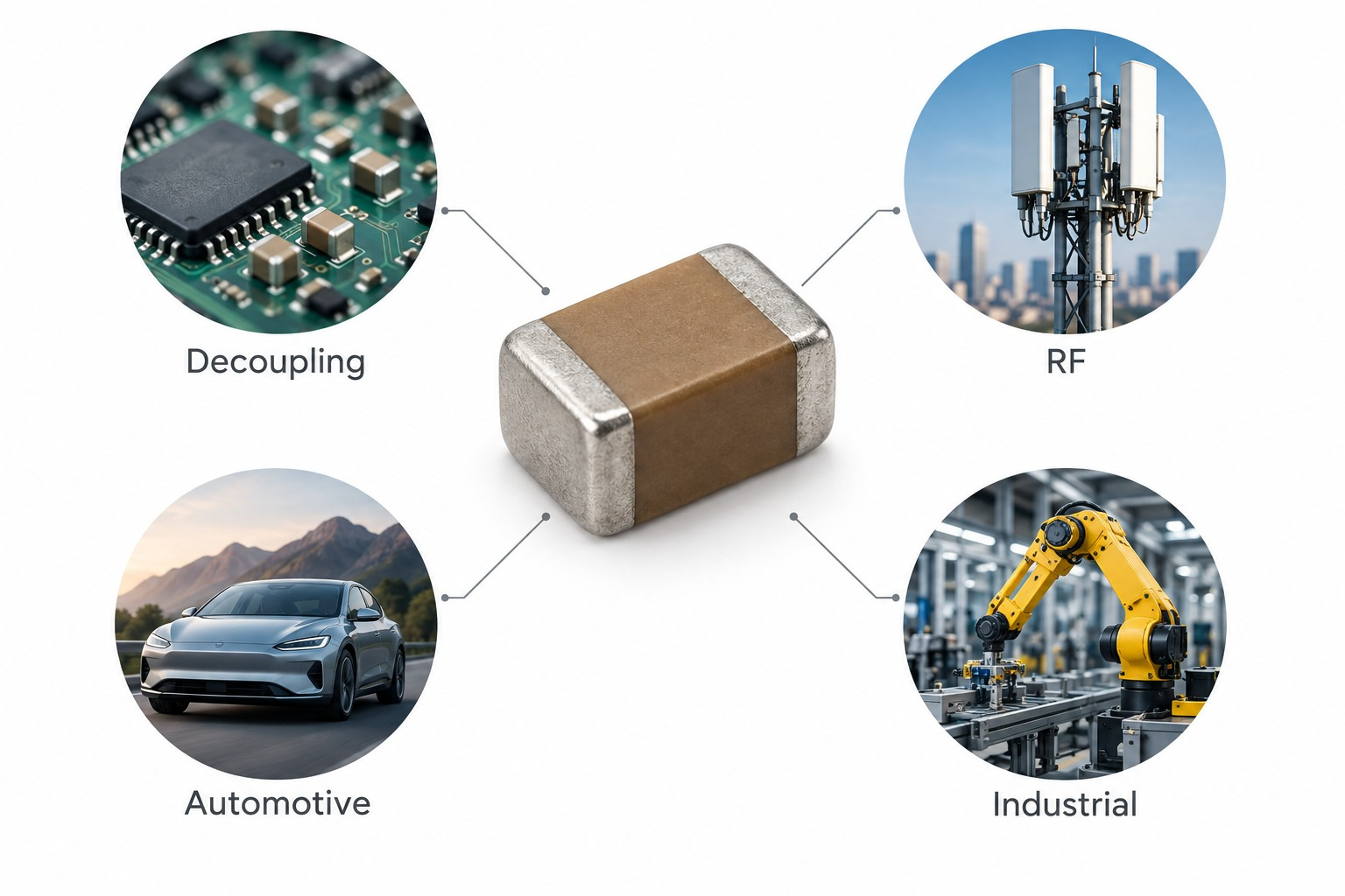
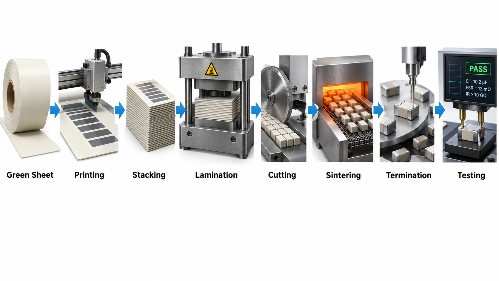
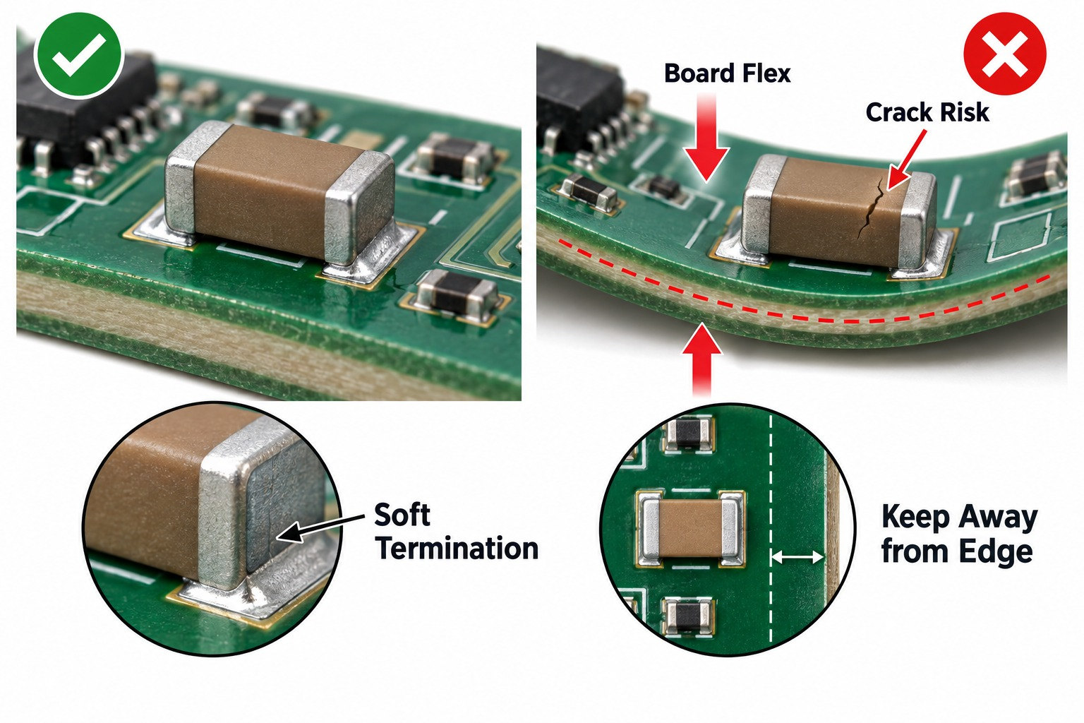
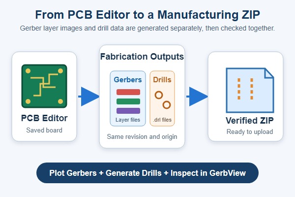
Electronics manufacturing services Switzerland buyers can choose from include local engineering specialists, PCB assembly companies and full-service manufacturing groups. The right partner should fit your technical requirements, budget and delivery schedule. This guide compares ten providers and introduces EBest Circuit (Best Technology), a China-based PCB and PCBA partner that completed production and dispatch for a Swiss medical electronics project within 1.5 weeks.
Top 10 Electronics Manufacturing Companies in Switzerland
Whether you need product development, assembled circuit boards or complete-device manufacturing, the following shortlist provides a starting point for comparing Swiss EMS providers.
This Top 10 is a purchasing shortlist, not a ranking by revenue or quality.
Custom coils, component assemblies and related EMS services
The most suitable provider depends on the work involved. A custom-coil project needs different expertise from a conventional PCBA order, while complete-device manufacturing adds enclosure, wiring and integration requirements.
Some providers operate international production networks. If Swiss manufacturing is mandatory for your product, confirm the proposed production site before comparing prices.
How Does Electronic Manufacturing in Switzerland Compare with China?
Swiss production offers proximity. Chinese production provides an overseas sourcing option that can be evaluated on manufacturing scope, capacity and total delivered cost.
Comparison
Swiss Manufacturing
Chinese Manufacturing
Engineering collaboration
Convenient on-site access
Remote technical support
Cost assessment
Local service and replenishment value
Manufacturing and landed costs
Location requirements
Swiss-production projects
Projects permitting overseas sourcing
Delivery
Local coordination
Cross-border shipping required
Local manufacturing can be valuable when your engineers need frequent hands-on access to early builds. Overseas production is worth comparing when the design is documented and your customer permits manufacturing outside Switzerland.
For buyers seeking an integrated overseas option, EBest combines PCB fabrication, component purchasing and PCBA assembly. This reduces the need to coordinate separate suppliers for each stage.
The meaningful comparison is the cost of the same finished deliverableānot a tested, delivered PCBA quotation against an assembly-only factory price.
How Do EMS Manufacturing Costs Compare?
At EBest, we review the PCB specification, BOM, quantity and assembly requirements together. This helps identify what is driving your quotation and where a different purchasing or manufacturing choice may reduce cost.
The main opportunities depend on your project:
Separate setup costs from repeat costs. Stencils and fixtures can make a small first order relatively expensive. Showing them separately makes future batch costs easier to understand.
Review the BOM before purchasing. Our component sourcing support can identify availability issues and proposed alternatives for your engineers to assess.
Compare quantities without hiding inventory costs. A larger material purchase may reduce the component price but leave unused stock. That commitment should be visible.
Include the work you actually need. Programming, testing and packaging should be included in the comparison when they are part of the required delivery.
For example, a lower assembly-only quotation may look attractive until your team adds programming, inspection and handling costs. Conversely, paying for a test you already perform effectively in-house may not add value.
Our DFM and BOM reviews focus on manufacturability and purchasing choices before production. Any proposed design or component change remains subject to your approval.
Send EBest your files and expected quantities to receive a quotation matched to your project rather than a generic price estimate.
How Can You Shorten Production Lead Times?
EBest offers standard and expedited production options to help Swiss customers plan prototype and assembly orders. For qualifying FR4 bare-board prototypes, our fastest service starts at 24 hours for one- and two-layer boards.
FR4 prototype lead times:
Layers
Normal Service
Fastest Service
1
7 days
24 hours
2
8 days
24 hours
4
10 days
48 hours
6
10 days
72 hours
8
12 days
72 hours
10 or more
Quoted individually
Quoted individually
These times apply to prototype orders below 1 m² meeting our standard FR4 specification: 0.4ā1.6 mm thickness, H/H or 1 oz copper, lead-free HAL, green solder mask and white silkscreen, with trace width and spacing above 8 mil, minimum holes above 0.3 mm and minimum annular rings above 10 mil.
PCBA service reference:
Service
Normal Service
Fastest Service
PCBA
1 week
2 days
PCBA timing is confirmed after reviewing component availability, fabrication needs, assembly complexity and testing requirements. The two-day option is not a blanket promise for a complete turnkey order starting from unpurchased materials.
For Swiss customers, shipping time is additional. Our quick-turn PCB assembly team can assess your files and required date to identify an appropriate production option.
The medical project below provides a separate example: EBest completed production and dispatched the boards within 1.5 weeks. Its 0.3 mm board thickness falls outside the standard FR4 prototype range above, so it should not be treated as a 24-hour standard-specification order.
What Quality and Testing Evidence Should You Request?
EBest Circuit (Best Technology) holds ISO 9001, ISO 13485, IATF 16949 and AS9100D certifications. For Swiss customers evaluating a manufacturing partner, these credentials support supplier qualification alongside the technical requirements of the specific project.
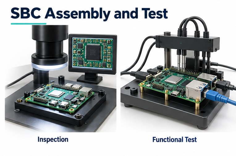
Our inspection and testing capabilities include the following, as listed in our company product catalogue:
Inspection or Test
Purpose
SPI
Check solder-paste deposits before component placement
AOI
Inspect component placement and visible soldering defects
X-ray inspection
Examine hidden solder connections where required
ICT
Check applicable circuit connections and component characteristics
Functional testing
Verify agreed operating functions against defined limits
We match the inspection and test scope to your assembly. Not every order needs every method, and functional testing requires an agreed test specification and any necessary fixtures or software.
For medical electronics projects, ISO 13485 is relevant to quality-system evaluation; it does not replace finished-device approval. We can discuss the applicable certification scope and required quality records with your team before production.
This gives you a clearer basis for assessing both the supplier and the boards you will receive.
How Can EBest Support Your Swiss PCB and PCBA Projects?
EBest provides a China-based manufacturing option for Swiss customers who need PCB fabrication, component procurement and assembly within one coordinated order.
Our support is built around practical customer benefits:
Fewer supplier handovers: combine PCB manufacturing, sourcing and PCBA assembly instead of managing separate providers.
Direct technical support: one sales contact works with three engineers to address quotation and manufacturing questions together.
Earlier cost and manufacturing review: DFM analysis and BOM review help identify issues before materials and production time are committed.
Flexible order sizes:prototype PCB assembly and small-batch support let you evaluate a build before increasing quantities.
Production options matched to your deadline: standard and expedited services can be assessed against the actual board and assembly requirements.
You do not need to commit to a large production order to begin the discussion. Send your current files, quantity and target date, and our team can review the scope, identify outstanding technical questions and prepare a project-specific quotation.
Case Study: How EBest Supports Swiss Electronics Projects
A Swiss medical electronics customer needed an internal connection or adapter board for a medical device. The board provided an electrical interface between parts of the equipment, making its physical dimensions and assembly requirements important to the project.
EBest handled PCB manufacturing, component purchasing and SMT assembly, giving the customer one manufacturing partner for the board and assembled components.
Project at a glance:
Item
Project Detail
Application
Internal connection or adapter board for medical equipment
Construction
Two-layer FR4
Board thickness
0.3 mm ±0.1 mm
Copper and finish
0.5 oz copper, immersion gold
EBestās scope
PCB fabrication, component purchasing and SMT assembly
Production and dispatch
Completed within 1.5 weeks
The thin-board specification was a key part of the customerās design. EBestās scope brought that PCB requirement together with the components and SMT assembly needed for the medical-device connection module.
Production was completed and the boards were dispatched within 1.5 weeks, excluding transportation to Switzerland.
For the customer, the result was a completed manufacturing order covering both the PCB and its assembly, without separately coordinating board fabrication and component purchasing. For similar medical electronics projects, EBest can review the design, assembly scope and required date to determine a suitable manufacturing plan.
FAQs About Electronics Manufacturing Services Switzerland
Which EMS company in Switzerland is best for my project?
Choose according to the required deliverable. Product development, PCB assembly, complete-device manufacturing and specialist components require different capabilities. The shortlist above helps identify relevant providers; EBest offers a China-based alternative for projects permitting overseas production.
How quickly can EBest manufacture FR4 prototypes?
For standard-specification orders below 1 m², the fastest service is 24 hours for one- and two-layer FR4 bare boards, 48 hours for four layers, and 72 hours for six or eight layers. Non-standard specifications require an individual schedule.
Can EBest complete PCBA in two days?
Two days is our fastest PCBA service reference. Availability depends on the actual order, including material readiness, assembly requirements and testing. We confirm the applicable schedule after reviewing the project.
Does EBest support medical PCB and PCBA projects?
Yes. EBest holds ISO 13485 certification and supports PCB manufacturing and assembly for medical electronics projects. The Swiss case in this article involved an internal medical-device connection or adapter board.
Does the quoted production lead time include delivery to Switzerland?
Production and shipping are separate. The Swiss medical project was completed and dispatched within 1.5 weeks; that period did not include transit to the customer.
What should I send for a quotation?
Send Gerber files, the BOM, assembly drawings or placement data, order quantity and target delivery date. Include programming and testing requirements where applicable.
Ultimately, your next supplier should offer more than a competitive price: you need manufacturing capability, a realistic schedule and quality support suited to your product. If you are comparing electronics manufacturing services Switzerland options with overseas production, send your files to sales@bestpcbs.com. EBest Circuit (Best Technology) can review your PCB and PCBA requirements and quote a manufacturing option for your next order.
An IMS PCB PCBA manufacturer can help you turn your board design into an assembled product with fewer supplier handoffs. For insulated metal substrate (IMS) boards, reviewing fabrication, components, and assembly together helps catch mismatches before they interrupt production.
EBest Circuit (Best Technology) combines metal-core PCB manufacturing, component sourcing, and SMT assembly, so you can order bare boards or bring these stages together with one supplier. Email your available files and project requirements to sales@bestpcbs.com. We can review what you have and help identify the next steps toward a quote.
Bare IMS boards and assembled LED boards in one manufacturing workflow. AI-generated illustration.
What Can You Order from an IMS PCB PCBA Manufacturer?
You can keep your existing assembly arrangement or have EBest handle fabrication and assembly together. The right choice depends on the work you want to keep in-house and what you need delivered.
Choose the supply arrangement that fits your project:
Service
Includes
Best fit
Bare IMS PCB
Board fabrication
Existing assembly partner
PCB + components
Bare boards and purchased parts
Coordinated material supply
PCB + SMT assembly
Fabrication and assembly
Customer-supplied or mixed parts
Turnkey IMS PCBA
PCB, parts, and assembly
One manufacturing supplier
Optional services
Testing, cleaning, or wiring
Additional delivery requirements
Clear pricing makes these options easier to compare. During quotation review, we can clarify which components, tooling, tests, depaneling, and packaging are included, helping you budget for the finished order rather than just the bare board.
Bare and assembled aluminum-core boards illustrate two supply options. AI-generated illustration.
Can Your IMS PCB Material Meet Your Assembly Requirements?
Reviewing the material and assembly requirements together can help you avoid buying boards that need changes before they can be assembled. The key is to check the board construction, surface finish, and component requirements before fabrication starts.
An IMS board combines a metal base, a thermally conductive insulating layer, and circuit copper. Two boards described as āaluminum PCBā may still have different insulation layers, copper weights, and thicknesses. Reviewing these details against your design helps establish whether the proposed board meets your manufacturing requirements.
An early review helps address five common sources of rework:
Material mismatches. Checking the metal base, insulation layer, copper weight, and thickness against your design helps prevent an unsuitable substitution.
Soldering conflicts. Reviewing board and component temperature limits together helps identify restrictions on the assembly process.
Finish and storage issues. Confirming the surface finish and handling requirements helps plan how boards will be stored before soldering.
Installation problems. Mounting holes, connector access, component height, and heat-sink clearances need to match the intended assembly.
Panel changes. A panel suitable for fabrication may need adjustments for component placement or separation after assembly.
If a material detail is still open, share the drawing or existing specification. EBest can flag questions for your engineering team before purchasing begins. This manufacturing review supports your design; final thermal performance still needs validation in the finished product.
Why Choose EBest Circuit as Your IMS PCB PCBA Manufacturer?
With EBest, you can discuss the bare board, purchased parts, and assembly in one place. That means less work transferring requirements between suppliers and a clearer view of what your order includes.
Here is how that helps your project:
Less coordination between suppliers. Fabrication and assembly questions can be reviewed together, reducing the information you need to relay between separate companies.
Flexibility over component supply. You can discuss full sourcing or retain control of selected parts through a mixed-supply arrangement.
Fewer gaps between fabrication and assembly. Board construction, panel layout, component placement, and delivery format can be reviewed within the same order.
Whether your priority is fitting an existing housing, keeping specified components, or meeting a prototype deadline, sharing that priority early helps focus the review on what matters to your project.
Illustrative SMT placement of LED components on an aluminum-core PCB. AI-generated illustration.
How Soon Can You Receive Your Assembled Boards?
If you have a prototype deadline, EBest can review normal and expedited production options against your target date. Standard single-layer aluminum MCPCB prototypes have a reference fabrication time of 4 days, or 24 hours for eligible expedited orders. PCBA has a separate reference of 1 week, with an expedited option of 2 days.
Use these production times for initial planning:
Stage
Normal
Fastest
1-layer MCPCB
4 days
24 hours
2-layer MCPCB
14 days
168 hours
4-layer MCPCB
21 days
To confirm
PCBA
1 week
2 days
The MCPCB references apply to prototype orders totaling less than 1 m², using standard aluminum material, 0.8ā2.0 mm thickness, the listed standard copper options (H/H or 2 oz), lead-free HASL, white solder mask, black silkscreen, and 0.8 W/(mĀ·K) thermal conductivity. Different materials, constructions, or finishes require a project-specific schedule.
For your assembled order, EBest can confirm a schedule covering fabrication, component sourcing, assembly, and inspection. A 24-hour board service and two-day assembly service are separate options, not an automatic three-day turnaround. The combined schedule depends on available capacity, component readiness, and approved production files.
Have a fixed arrival date? Include it with your inquiry so production and shipping can be considered separately before you commit to the order.
What Inspection and Test Reports Will You Receive?
The most useful reports are those that help your team accept the boards and move to the next stage. That may mean confirming dimensions for installation, reviewing hidden solder joints, or checking that an LED assembly operates before system integration.
EBest’s PCB inspection services include electrical testing, AOI, X-ray inspection, and assembly quality checks. The methods and reports for your order can be agreed during quotation review.
These checks can help you assess the boards before acceptance:
Check
What it checks
Details to agree
Board electrical test
Continuity and isolation
Coverage and report format
Dimensions
Drawing compliance
Critical dimensions and tolerances
Assembly inspection
Placement and visible joints
Workmanship and critical features
X-ray, if needed
Hidden-joint inspection
Packages, criteria, and images
Functional test
Operation under test conditions
Test setup and pass/fail limits
Final checks
Cleanliness and delivery format
Residue, labels, and packaging
You can start by sharing your drawing and any existing acceptance checklist. For functional testing, we can review the power input, procedure, fixtures, and pass/fail limits with your team. The review can also cover panel or individual-board delivery and any medical-project records needed for the order and revision.
An LED operation check helps you verify board-level function. Thermal performance and service life require separate validation under the finished product’s operating conditions.
Illustrative optical inspection of board mounting-hole positions. AI-generated illustration.
IMS PCB PCBA Case Study: From Customer Requirements to Delivery
A surgical-lighting customer needed an assembled LED board, not just a bare aluminum PCB. EBest handled the aluminum-core board fabrication, component procurement, and SMT assembly, completing the project within 1.5 weeks.
The customer needed boards that could move on to installation in the lighting assembly. Alongside electrical operation, the order addressed LED placement, mounting-hole positions, and cleanlinessādetails that matter when the PCBA is fitted into the light.
The project at a glance:
Item
Details
Application
Surgical-lighting LED board
Construction
Single-sided aluminum-core PCB
Thickness
1.6 mm ±10%
Copper
1 oz
Finish
Lead-free tin
Mask / legend
Black / gray
Scope
PCB, component sourcing, SMT
Approval items
Panel data and stack-up
Completion
Within 1.5 weeks
Customer approval of the panel data and stack-up was required before production.
To help the LED board fit and function in the surgical-lighting system, we focused on four areas:
LED positions that follow the optical layout. The order highlighted LED placement offset, helping keep assembly focused on the positions in the customer’s approved design.
Mounting holes checked before installation. Optical measurement of hole positions was required before shipment to check alignment with the intended mounting points.
LED operation checked before system integration. The assembly instructions required all LEDs to be checked for operation before shipment, giving the customer a board-level check before installing the PCBA in the light.
Boards cleaned for delivery. The order specified cleaning and control of solder balls, rosin, and other residue as part of the delivery requirements.
This brought the bare board, purchased components, and assembly into one order, with linked PCB and SMT records and documented pre-shipment requirements. The completion time applies to this build; other projects are scheduled according to their specifications and component availability.
These checks covered the board, while the complete surgical light still needed its own optical, thermal, and lifetime validation.
For a similar lighting project, tell us where the board will be installed and which positions or dimensions are critical. We can review those details alongside your PCB and assembly files.
Surgical-lighting application illustration; not a photograph of the customer project. AI-generated illustration.
How Can You Request an IMS PCB Quote for Your Project?
You do not need every detail finalized before contacting us. Send your available PCB files, expected quantity, and whether you need bare boards or assembled boards. For assembly, include your current BOM if available. EBest can review the information and identify what else is needed to prepare your quote.
Start with what you have:
Available PCB files or drawings;
expected order quantity;
bare-board or assembly requirements;
target delivery date and destination.
Materials, component availability, and testing can be clarified during the review. If a part or material must remain unchanged, let us know so it stays central to the quotation. Before production, the fabrication files, BOM, placement data, and agreed acceptance requirements will need to be confirmed.
The quotation can separate fabrication, components, assembly, tooling, testing, and shipping where applicable, making it easier to see what you are paying for. Final pricing and lead time follow once the key requirements are confirmed.
Email your available project information to sales@bestpcbs.com. You can begin the conversation now and work through the remaining details during the review.
FAQs About IMS PCB PCBA Manufacturer
Can I order only the bare IMS PCB?
Yes. You can order bare boards and keep your existing assembly partner. EBest can review that partner’s panelization, finish, and handling requirements as part of the fabrication inquiry.
Can EBest purchase the components as well as manufacture the board?
Yes. You can bring fabrication, component sourcing, and assembly into one order. Your current BOM is a useful starting point; manufacturer part numbers and sourcing responsibilities can be clarified during review.
Can I supply selected components?
Yes, a mixed-sourcing arrangement can be reviewed for your project. Let us know which parts you want to supply, and we can review quantities, packaging, and arrival timing before finalizing the assembly schedule.
Can I request expedited IMS PCBA production?
Yes. Share your target arrival date and available files. EBest can review expedited options against board specifications, component availability, quantity, testing needs, and production capacity. The complete schedule is confirmed for your order, with shipping time identified separately.
Does a functioning LED board prove that the finished product meets its thermal requirements?
A working LED board confirms operation under the test conditions. To assess thermal performance in the finished light, a separate test needs to reflect the enclosure, cooling arrangement, and operating conditions.
Can you replace an unavailable component with an equivalent?
EBest can help identify alternatives for your review. Your team approves the replacement before purchase, keeping control of changes that may affect fit, performance, or reliability.
Looking for an IMS PCB PCBA manufacturer for your next build? Send what you have to sales@bestpcbs.comāwhether that is a board drawing, a BOM, or an existing manufacturing package. EBest can help you take the next step toward a fabrication-and-assembly quote.
The latest Kingboard price increase concerns the materials used to manufacture PCBs, not an automatic increase in every finished-board quotation. An August 28, 2026 notice reproduced by financial media reports higher FR-4 and prepreg prices for newly accepted orders. For purchasing teams, the next step is to identify the material used in each board and confirm which commercial terms apply.
At EBest Circuit, we help customers review PCB material requirements alongside fabrication needs. This update explains the reported changes, where they enter a multilayer board’s material bill, and what to clarify when a supplier sends a revised quotation.
What Changed in the August 28 Notice?
Gelonghui’s August 28 report, carried by Sina Finance, reproduces a notice from Guangdong Kingboard Laminates Trading Co., Ltd. The stated adjustments are:
Material category in the notice
Reported increase
FR-4, all thicknesses
10%
Prepreg: 7628 and the notice’s thicker-cloth category
10%
Prepreg: the notice’s thin-cloth category below 7628
20%
The reproduced letter is dated August 28. We checked its wording against the report, but it was obtained through a media publication, not a direct supplier communication. Confirm the applicable grade and price with your material supplier before changing a purchase order.
When Does the New Pricing Apply?
The notice refers to new orders accepted from its issue date. It does not establish how every distributor will handle existing inventory, previously accepted orders, or an earlier quotation that remains valid.
Before approving a revised board price, ask for three specific confirmations:
Order status: Was the material order already accepted, or does the job still require a new purchase?
Quotation basis: Which material grade, copper weight, sheet size, quantity, currency, and tax basis are being compared?
Validity: How long does the revised quotation remain open, and what event fixes the price?
A finished-PCB purchase order and a laminate manufacturer’s order are different transactions. Do not assume that sending a board PO earlier automatically secures an earlier material price; obtain written confirmation from the party supplying your boards.
Why Are Glass Cloth and Copper Foil Important?
The letter cites rising prices and tighter supply of glass cloth and copper foil. Both are inputs to PCB laminate production; neither is simply an optional accessory that can be removed from a drawing.
A copper-clad laminate combines a dielectric base with copper foil. Prepreg supplies resin-bearing reinforcement between layers during lamination. Their costs enter the material bill through different purchased items and constructions.
The notice alone does not tell us how much either input has risen across the entire market, how long supply pressure will last, or which next adjustment will follow. Those would require separate dated evidence. For a current order, the relevant information is the supplier’s quotation for the exact material being purchased.
PCB Prepreg vs Core: Which Material Is Affected?
The distinction in PCB prepreg vs core matters because a multilayer stackup uses cured laminate and bonding sheets differently. A core is already cured; prepreg starts as resin-impregnated reinforcement that bonds the assembly during pressing.
For background on the bonding stage, see our explanation of prepreg in PCB manufacturing. For this price review, identify the actual core and prepreg entries in the approved stackup rather than treating the entire board as a single sheet of FR-4.
When comparing prepreg PCB material, retain the manufacturer’s grade, resin system, glass style, resin content, and number of plies. Two options described simply as āFR-4 prepregā may not have the same electrical properties or processing behavior. A purchasing description that omits these details can hide a construction change inside an apparently cheaper quotation.
Why Does Prepreg PCB Thickness Need a Construction Check?
Prepreg PCB thickness is not determined by a glass-style number alone. Resin content, the selected construction, and the pressed assembly all matter. Manufacturer data can list more than one thickness or resin-content option for the same glass style.
The notice’s wording around 7628 is a supplier pricing category. It should not be converted into a universal rule that every glass-style code with a smaller numerical value is physically thinner. Match each ordered prepreg item to the supplier’s classification.
Construction also affects PCB prepreg dielectric constant. Isola’s laminate-manufacturing guide explains that glass construction and retained resin content influence dielectric properties. Its material data illustrate why an apparently similar glass designation is not enough to prove equivalence; those Isola values should not be copied into a Kingboard design.
For an impedance-controlled board, changing dielectric spacing or material properties can require a new impedance calculation and an approved stackup revision. Keep the electrical requirement fixed while evaluating the material choice.
Does a 20% Prepreg Increase Mean a 20% PCB Price Increase?
No. A percentage applied to one purchased material does not automatically apply to the total selling price of a finished PCB. The board also includes other materials, fabrication operations, inspection, testing, handling, and commercial terms.
A useful calculation starts with the affected material lines, not the total board invoice: multiply each old material-line cost by its applicable adjustment, then add the differences. That estimates the change in those lines only, assuming the same specification, quantity, and purchasing basis.
It still does not determine the final commercial quotation. Inventory purchased at an earlier price, panel utilization, production volume, and other cost changes may affect the outcome. Our copper-clad laminate price guide provides broader background on material-price factors.
If a revised quotation cites the Kingboard price increase, ask which material lines changed and whether the board specification stayed the same. A traceable explanation is more useful than applying a headline percentage to every item.
Which Cost-Saving Changes Need Engineering Approval?
Start with options that preserve the approved design, such as reviewing order quantities or panel utilization with the fabricator. Material substitutions require a separate technical decision; a lower material price does not establish that the replacement will work.
Changing prepreg construction: Review finished dielectric spacing, resin availability around copper features, and electrical requirements.
Changing laminate grade: Compare the relevant thermal and electrical properties and any material restrictions on the drawing.
Reducing copper: Recheck current handling, thermal behavior, and fabrication requirements rather than treating copper weight as a purchasing-only choice.
Changing a qualified build: Agree on required samples, inspection, and customer approval before production release.
Keep the existing approved construction if equivalence has not been demonstrated or the customer does not permit substitutions. Requalification time and scrap risk can outweigh a small purchase-price saving.
How Can We Help You Review a Material-Cost Change?
At EBest Circuit, we provide PCB fabrication and PCBA services with technical support for material and build requirements. We can review your approved stackup and discuss which material choices are fixed, which alternatives may be evaluated, and what information is needed for a current quotation.
Send your Gerber files, stackup, specified laminate grade, copper weight, order quantity, and required delivery date to sales@bestpcbs.com. If you are comparing a revised quote, include the earlier specification and quote date so we can compare the same build. Any proposed material change should be documented and approved before manufacturing.
The Panasonic laminate price increase announced on August 6, 2026 takes effect for September 1 shipments on an ex-factory basis. This August 31 update is an execution reminder, not a new price announcement. The change covers several circuit-board material categories, with different rates for general glass-epoxy and low-loss products.
For PCB buyers, the practical questions are which material their approved build uses, when that material ships, and whether a revised quotation still describes the same board. At EBest Circuit, we can review those technical requirements with you before a proposed substitution changes the build.
Which Panasonic PCB Materials Are Included?
Panasonic Industry’s official notice lists the following changes from current material prices:
Material group
Affected products
Increase
General multilayer glass epoxy
Laminate and prepreg
30%
MEGTRON / XPEDION
Laminate and prepreg
15%
LEXCM GX substrate materials
Laminate and prepreg
30%
CEM-3
Glass-composite materials
30%
FCCL
Flexible circuit-board materials
15%
These are Panasonic PCB materials, not replacement control boards for air conditioners or other appliances. Package-substrate materials, flexible materials, and ordinary rigid-board materials should also remain separate entries in a purchasing review. A rate for one category should not be applied to another simply because both are used somewhere in electronics manufacturing.
When Does the September Revision Take Effect?
The stated trigger is shipment from the factory from September 1, 2026. It is not described as a deadline based only on when a customer submits a purchase order.
For a board buyer, the laminate shipment date, PCB production start, and finished-board delivery date are three different milestones. Ask the fabricator which material transaction applies to your order rather than inferring it from your requested PCB delivery date.
Material already allocated: Confirm the allocation, quantity, and applicable quotation in writing.
Material still to be purchased: Obtain a current quote and an expected material shipment date.
Repeat orders or scheduled releases: Check whether each release has its own purchasing and pricing conditions.
A quotation’s validity period is not the same as a stock reservation. If the supplier cannot confirm allocation, do not treat material availability or an earlier price as secured.
Why Is Panasonic Revising Material Prices?
Panasonic cites sustained increases in principal raw materials, together with elevated auxiliary-material, energy, logistics, and other costs. The notice presents the revision as necessary to support continued supply.
That explanation does not provide a PCB-fabricator cost breakdown. A board quotation includes more than the purchased laminate and bonding sheets. The affected material share, processing route, quantities, and contractual terms must be reviewed for the specific order; no finished-PCB price increase can be calculated from the announcement alone.
Nor does a price notice establish that every material grade is unavailable. Treat price, stock allocation, and lead time as separate questions. A higher price is not proof of an earlier delivery slot, and an available sample sheet is not proof of production-volume availability.
What Does This Mean for Panasonic MEGTRON 6 and 7?
Panasonic MEGTRON 6 and Panasonic MEGTRON 7 are material families used in high-performance multilayer boards. They should be identified by the exact laminate and prepreg grades on the approved stackup, not just the family name.
A common percentage adjustment does not make two grades equal in absolute price or technically interchangeable. Their earlier prices, constructions, and processing requirements can differ. A purchasing comparison must retain the grade suffix, copper foil, dielectric construction, panel requirements, and order volume.
For high-speed designs, changing the dielectric system is a signal-integrity decision as well as a cost decision. Channel loss and impedance depend on the board construction and routing, not on the material trade name alone. Our high-speed PCB design guidance explains why the full interconnect needs attention.
If the drawing explicitly specifies a manufacturer and grade, keep that requirement in the quote. Present any alternative as a separate option requiring approval, not as an equivalent silently substituted during purchasing.
What Should You Check in a Panasonic MEGTRON 6 Datasheet?
A Panasonic MEGTRON 6 datasheet is useful for confirming which product a quotation actually refers to. The manufacturer’s documentation distinguishes laminate variants such as R-5775(N), R-5775(K), and R-5775(G), with corresponding R-5670 prepregs. It also identifies typical values and the conditions used to measure them.
Exact product: Match the complete grade and suffix, including the associated prepreg.
Electrical data: Compare Dk and Df only with their frequency, method, and sample conditions stated.
Thermal data: Check that the property and test method match the assembly requirement being evaluated.
Copper and construction: Retain the specified foil and dielectric details when comparing transmission performance.
Do not take a typical datasheet result as a guaranteed acceptance limit for every finished board. Define the relevant build and inspection requirements separately. For the role of the bonding material, our PCB prepreg overview provides a useful starting point.
Can a Different Laminate Reduce Cost Without Changing Performance?
Possibly, but that requires evidence for the actual design. A material with a lower quoted sheet price can still require a stackup change, trace-width adjustment, process review, or additional qualification.
Start by fixing the performance and customer requirements that cannot change. Then compare candidate materials against those requirements, estimate the work needed to approve the change, and obtain written customer acceptance before release.
Our stackup and impedance-control guidance is relevant when dielectric thickness or properties change. Price comparisons should not leave the stackup as an unspecified item to be decided after ordering.
Keeping the existing material may be the better choice when a product is already qualified, the delivery window cannot accommodate validation, or the expected saving is smaller than the change effort. The purpose of a review is to make that tradeoff visible, not to assume that a substitute is always available or worthwhile.
What Should Be Confirmed for September Deliveries?
Ask for a written order confirmation that connects the material, price, and schedule. āMaterial availableā is too broad if the required grade, thickness, copper foil, or quantity is still unresolved.
Approved laminate and prepreg part numbers, plus any permitted alternatives.
The material allocation and expected factory shipment relevant to your job.
The quotation date, validity, and treatment of scheduled releases.
The expected PCB delivery date after material receipt and fabrication.
Who approves a material change and what validation is required.
When discussing the Panasonic laminate price increase internally, keep the supplier’s material notice separate from your project’s board quotation. That gives engineering and purchasing the same documented basis for approval.
How Can EBest Circuit Help With Your Material Review?
At EBest Circuit, we support PCB fabrication and PCBA projects, including multilayer and high-speed board requirements. We can review your specified materials and stackup, clarify which requirements must remain fixed, and discuss alternatives that may merit engineering evaluation.
Email sales@bestpcbs.com with your Gerber files, approved stackup, full laminate and prepreg grades, quantities, and target delivery date. Include any customer restrictions on substitution. We will use those requirements to discuss a current quotation and the review needed before changing the build, without treating a material-price headline as a finished-board price.
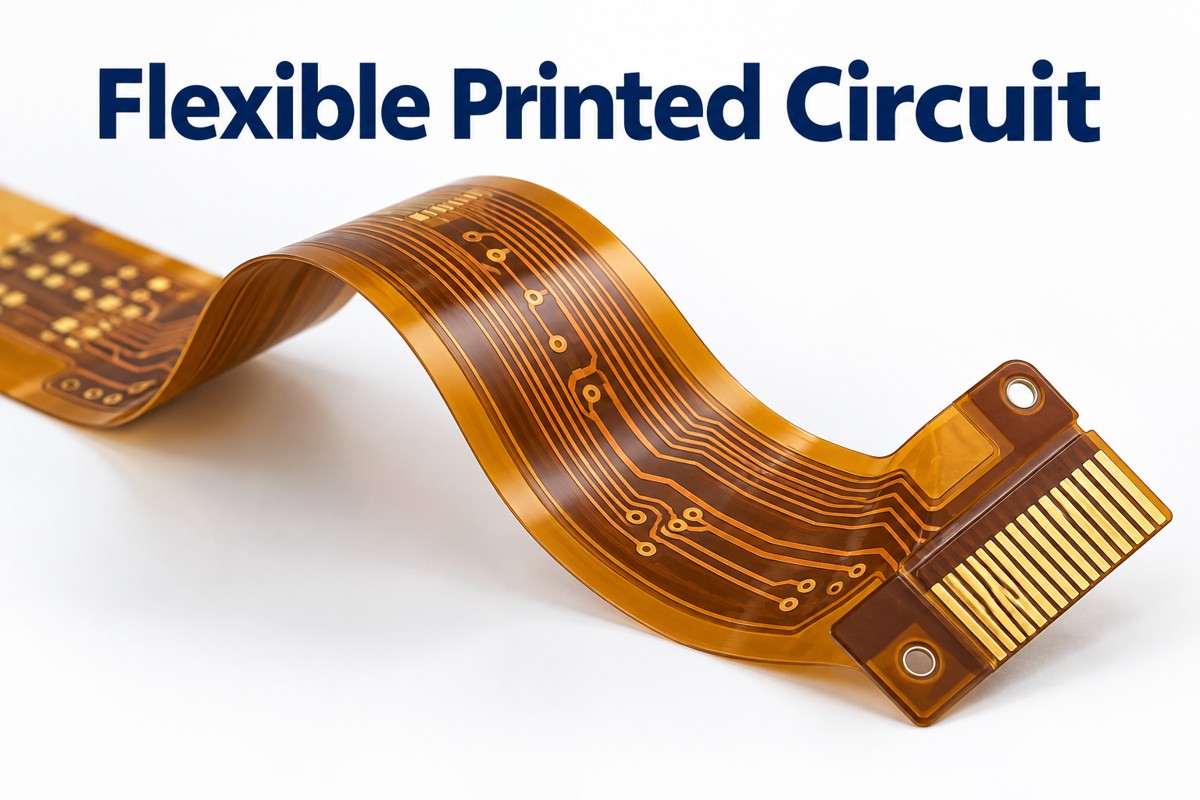
PCB board stiffeners are supports that reinforce selected areas of a printed circuit board without turning every flexible section into a rigid board. In flexible circuits, they commonly support connectors, component mounting areas and contact fingers. In assembly equipment, the same term can describe removable supports that hold a board during processing. Choosing the right construction starts with separating these two jobs, then checking material, bonded thickness and the forces at each support edge.
What Is Stiffener in PCB?
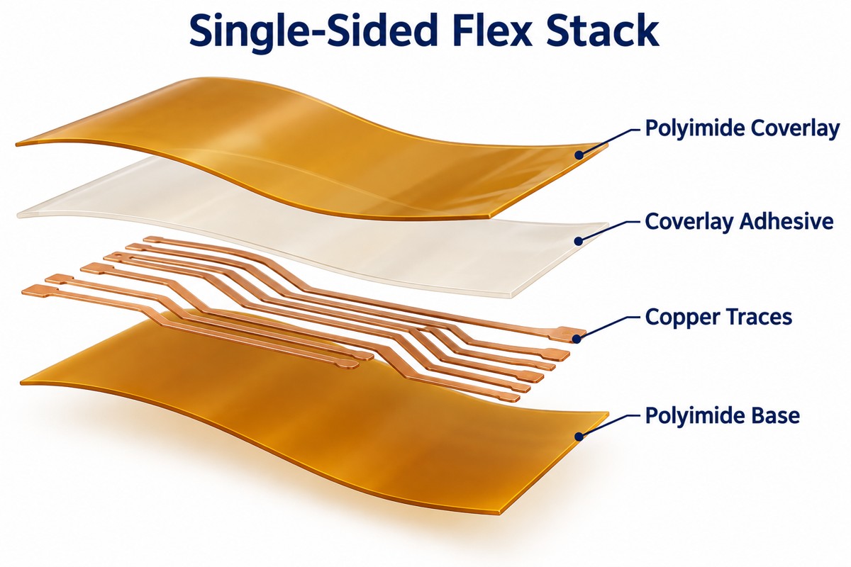
A PCB stiffener is an added mechanical layer, not an extra signal-routing layer. An FR4 backing piece can keep a connector area flat, while a polyimide backing film can bring a flexible contact tail to the thickness required by its socket. The electrical conductors remain in the circuit, rather than in the ordinary stiffener.
A circuit board stiffener is therefore different from increasing copper weight or adding another conductive layer. The components of PCB board assemblies still need electrically sound pads, traces and joints; reinforcement only changes their mechanical support. FPC stiffener and flex circuit stiffener are names used for this local reinforcement on flexible printed circuits.
How Can You Stiffen a PCB?
For a flexible circuit, bond a suitable backing to the area that must resist handling or connector loads. For a rigid assembly, consider its supports, fasteners, rail spacing or assembly fixture before changing the laminate. The useful question is where the force enters the board and where that force can safely leave it.
Connector area: resist insertion, extraction and cable-pull loads without bending nearby solder joints.
Component island: provide stable support beneath a populated flex area while leaving the intended bend zone flexible.
Contact tail: control mating thickness and handling stiffness without covering exposed contacts.
Assembly panel: reduce sag or handling movement with a carrier or removable panel stiffener.
A custom board stiffener should follow a defined load path. A larger backing is not automatically better: it can move bending into a shorter, more highly strained section of flex.
Which PCB Stiffener Material Should You Use?
Compare the mechanical job before comparing PCB board material types. FR4, polyimide and metal backings are not interchangeable merely because their outlines match. FPC stiffener material selection must also account for adhesive, insulation, temperature exposure and available height.
Material
Typical role
Important constraint
FR4 stiffener
Local support beneath connectors or component areas
Leaves a relatively abrupt rigid-to-flex transition; hole access and edge placement matter.
Polyimide stiffener
Thin backing for contact tails and local thickness adjustment
Provides less rigidity than a substantial FR4 backing; the complete bonded stack determines fit.
Stainless steel
Compact, high-rigidity reinforcement where the design justifies metal
Conductive edges need clearance or insulation; burrs and bonding surfaces require control.
Aluminum
Mechanical backing with a possible thermal role
Heat spreading depends on the actual interface and heat path, not the metal name alone.
For a steel board stiffener or copper board stiffeners, include the conductive backing in clearance and grounding reviews. A metal support must not accidentally bridge exposed pads or test points.
How Do You Choose PCB Stiffener Thickness?
PCB stiffener thickness must be selected together with the circuit and bond line. A finished contact tail is thicker than the backing alone. For a component island, the constraint may instead be allowable deflection, enclosure clearance or the height of a nearby mounting boss.
Finished supported thickness = flex-circuit thickness + cured adhesive thickness + stiffener thickness. Use the thickness of the actual local circuit region, including the layers present there. Do not add coverlay twice or assume that the contact-finger region matches the covered region.
Illustrative stack element
Nominal thickness
Local flex circuit
0.100 mm
Cured adhesive
0.025 mm
Selected backing
0.175 mm
Finished supported section
0.300 mm
This is an arithmetic example, not a stock material recommendation. If the respective tolerances were ±0.010, ±0.005 and ±0.015 mm, their worst-case sum would be ±0.030 mm. A nominal 0.300 mm result would then span 0.270-0.330 mm and would need to fit the connector’s permitted range.
PCB standard thicknesses for rigid boards do not establish the correct flex circuit stiffener thickness. The controlling requirement remains the selected connector drawing, not a generic PCB thickness value.
How Does a Flex PCB Stiffener Fit a ZIF Connector?
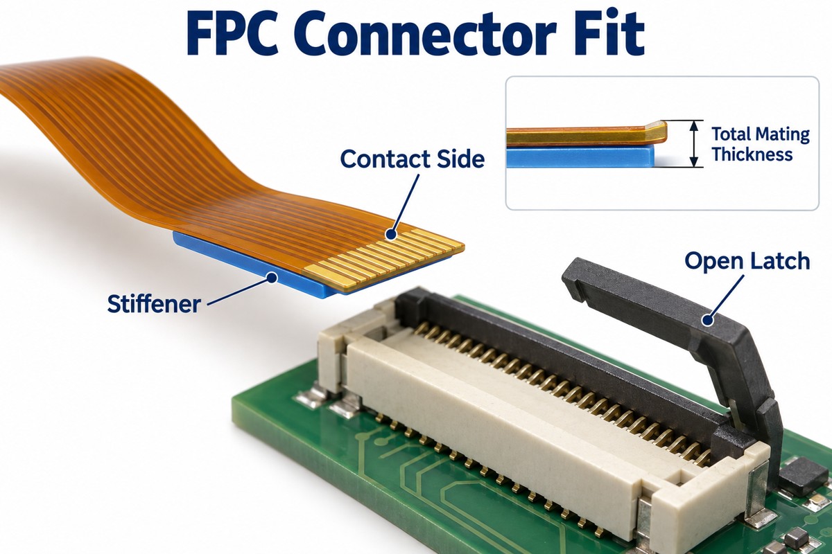
A ZIF connector needs the correct tail thickness, contact orientation, insertion length and outline. A flex PCB stiffener normally backs the non-contact side where the connector drawing requires it. It must not extend over the mating pads or obstruct the latch.
Check contact-side versus back-side orientation in a section view. Then verify the supported length, shoulder locations and available space after the latch closes. Too much thickness can obstruct insertion; too little can compromise retention or contact pressure. Neither condition should be corrected by forcing the latch.
A flex circuit with stiffener should be checked as a bonded assembly. Measure the finished tail at the specified location, then verify fit with the actual connector. Supplier examples of 0.20 mm or 0.30 mm tails are not permission to use those values for every socket.
Where Should Stiffeners End in Flex PCB Design?
Place the rigid boundary outside the intended active bend. In flex PCB design, an abrupt support edge can concentrate strain if the circuit repeatedly folds against it. Keep the supported island stable and provide enough free flex length for the required movement.
Stagger the coverlay termination and stiffener edge rather than aligning both boundaries at the same bend transition. Define the required overlap from the actual layer stack, fabrication tolerances and intended movement; one overlap dimension is not suitable for every construction.
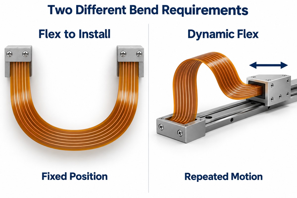
Practical flex PCB guidelines must distinguish a one-time installation bend from continuous movement. A support near a fold does not make the fold dynamically rated. Confirm the bending direction, radius, number of cycles and distance to pads or vias with the fabricator. Our custom flex PCB design guide discusses the wider layout context.
How Are PCB Stiffeners Bonded?
Common approaches use pressure-sensitive adhesive or a heat-and-pressure bonding process. The adhesive grade, surface condition and process sequence determine whether the joint is suitable; the label PSA by itself does not establish reflow compatibility.
Before bonding, control contamination, backing flatness and registration. During bonding, follow the qualified pressure, temperature and time for the chosen system. Afterwards, inspect edge lift, trapped air, misalignment and adhesive squeeze-out. The PCB board process must also define whether reinforcement is installed before or after high-temperature assembly.
Review the complete thermal history, including multiple soldering passes and any later rework. Moisture conditioning and permitted cleaning chemistry should follow the actual material data. Do not substitute household tape or assume that a room-temperature peel test predicts hot-process performance.
What Must a Stiffener Drawing Define?
Show the support as a controlled mechanical feature, not an informal note. PCB board dimensions alone do not tell the fabricator which side receives the backing or whether a dimension describes the backing itself or the finished assembly.
Identify backing material, nominal thickness and allowed tolerance.
Define the bond system and finished supported thickness where it is functional.
Dimension the outline, mounting holes and clearances from shared circuit datums.
Identify the top or bottom side and the relation to exposed contacts and coverlay.
Show bend keepouts, connector seating features and accessible inspection points.
An Altium flex stiffener design still needs an unambiguous fabrication view. A mechanical layer or 3D shape conveys geometry, but it does not automatically specify a bonding process or a qualified material. Check the exported files, not only the appearance in CAD.
In a plated through hole PCB, a conductive barrel belongs to the circuit. An ordinary backing clearance hole does not create an electrical interconnect. Size backing holes to allow for registration tolerance and solder access. Define the fabrication allowance on the drawing rather than assuming the backing and circuit holes should have identical diameters.
Stiffened Flex vs Rigid-Flex: What Is Different?
A printed circuit board stiffener provides support, whereas rigid-flex PCB construction combines electrically functional rigid and flexible sections. Bonding plain FR4 to a flex tail does not create plated connections to new rigid routing layers.
The distinction affects routing space, via structure, assembly access and validation. A support-only island can be sufficient for a connector. A design that needs dense routing or components on electrically integrated rigid sections may require a different architecture. Our rigid-flex PCB solutions integrate rigid and flexible circuit sections; they are not another name for a glued-on backing.
The term rigidflex describes the integrated construction; a stiffener board remains a mechanical support unless the design explicitly adds another electrical function.
Are PCB Edge Stiffeners the Same as Bonded Flex Backings?
No. PCB edge stiffeners used during assembly can be removable tooling. Titanium board stiffeners can clamp to PCB edges to support conveyor handling. Their function differs from a permanent reinforcement bonded beneath a flex connector.
A printed circuit board edge stiffener must leave components, conveyor features and required process access unobstructed. Board edge stiffeners and a carrier pallet also change how the board is supported during heating. Qualify that support arrangement with the actual assembly profile rather than treating the fixture as mechanically invisible.
For a thin panel stiffener, confirm whether it is retained in the product or removed after processing. We offer extra-thin PCB options at 0.15, 0.20, 0.25 and 0.30 mm. Those are board thicknesses, not standard stiffener thicknesses, and they make handling support an important design consideration. Panel support should be coordinated with PCB panelization and the assembly process.
What Can Go Wrong with a PCB Board Stiffener?
Observed problem
Possible contributor
Useful verification
Tail will not seat
Excess total thickness, wrong side or misplaced shoulder
Measure finished geometry against the connector drawing.
Cracks near the backing edge
Bending concentrated at a support boundary
Inspect the transition and repeat the actual motion while monitoring continuity.
Backing lifts after heating
Bond preparation, material compatibility or thermal-process issue
Review process records and inspect conditioned samples after the intended thermal sequence.
Intermittent contact to metal backing
Insufficient insulation or clearance
Check electrical isolation under expected mechanical loading.
Solder access is blocked
Backing holes or outline do not match assembly needs
Review the assembled section and inspect real solder joints.
A flat-looking board is not proof of reliability. Dimensional inspection, connector engagement, electrical continuity and application-specific mechanical testing address different failure modes. Record acceptance criteria before comparing samples so that a stronger backing does not hide a new transition failure.
How Does BestPCBs Support Reinforced Circuit Assemblies?
At EBest Circuit (Best Technology), we provide flexible circuits, rigid-flex boards and PCB assembly support. Our assembly capabilities include components as small as 01005 and BGA pitch down to 0.25 mm, subject to engineering evaluation. These capabilities do not replace reinforcement design: component placement, backing clearance and inspection access still need to work together on the actual assembly.
For a supported flex or thin-board assembly, the practical objective is a defined stack, an accessible assembly process and a verified mechanical interface. Discuss the circuit’s construction and intended motion with our engineering team at sales@bestpcbs.com.
Frequently Asked Questions
What does PCB stand for?
PCB stands for printed circuit board. A backing or stiffener supports the board but is not, by itself, a complete circuit.
Can you fix a bowed board with a stiffener?
Not reliably by simply forcing it flat. A support may limit deflection in a qualified design, but it does not repair cracked copper, damaged vias or delamination. Investigate the cause of bow and evaluate the board before applying force or heat.
Is a book binder flex PCB another type of stiffener?
No. Bookbinder construction uses separated flex layers with compensated lengths to accommodate different bend paths. It addresses multilayer bend geometry rather than adding local rigidity. Adding an extra backing layer does not reproduce this geometry.
Are through holes plated in a stiffener?
Ordinary mechanical backing holes need not be plated. They provide clearance or access, while electrical plated holes belong to the circuit design. The drawing must identify each hole’s purpose.
How do you choose material for stiffening PCB connector areas?
Start with the connector’s dimensions and forces. Then compare local rigidity, available height, electrical isolation and the bond system’s process compatibility. The best flex circuit stiffener material is the one that satisfies those constraints, not simply the thickest available backing.
Conclusion
Effective PCB board stiffeners support the areas that need stability while preserving the flex sections that must move. Select the material for its mechanical role, calculate the full bonded thickness, keep the transition out of the active bend, and verify the final assembly. Permanent flex reinforcement and temporary board-support tooling require different drawings and different checks.
SMT AOI uses automated optical inspection to check visible components and solder joints during surface-mount assembly. An SMT AOI machine can flag missing parts, incorrect orientation, placement offsets and visible solder defects. It does not prove that every connection is electrically sound, and it cannot see through a package to inspect hidden solder joints. Its value comes from combining repeatable visual checks with a defined defect-review process.
What Is AOI in SMT?
AOI is an optical inspection step, not a component-placement process. The AOI full form is automated optical inspection; SMT means surface mount technology. Together, the SMT AOI full form describes automated optical inspection used in a surface-mount production process.
The practical SMT AOI meaning is straightforward: compare the visible assembly with approved component, position and solder criteria, then route suspect locations for review. A camera image alone is not a pass/fail standard. The program must know which parts should be present, their polarity, and the allowed variation for the assembly.
How Does an SMT AOI Machine Work?
An AOI machine for PCB assembly captures controlled images, aligns them with the board data, and evaluates selected features. A typical inspection cycle has five steps:
Load and identify: select the correct board revision and inspection program.
Align: locate fiducials so inspection windows match the physical components.
Capture: use suitable lighting and camera views; a 3D system also measures surface height.
Evaluate: compare placement, markings and visible joint features with validated limits.
Review: confirm flagged defects, record the decision, and send affected boards for controlled repair or disposition.
SMT AOI inspection can use design data, component libraries and reference images. Reference boards must themselves be checked: copying a defective sample into the library can teach the system to accept the same defect again.
Where Does AOI Fit in the SMT Process?
The SMT AOI process is commonly placed after component placement or after reflow, with a different inspection objective at each position. Pre-reflow inspection checks placement before solder joints form. Post-reflow inspection checks the resulting visible assembly and exposed solder connections.
A typical SMT machine process is paste printing, solder paste inspection (SPI), placement, reflow and post-reflow AOI. An additional pre-reflow station may be useful when early placement feedback justifies the extra step. SMT line AOI should be positioned around the defects that need to be contained, rather than treated as a substitute for every other test.
Upstream control matters. The SMT stencil influences where paste is deposited and how much paste reaches each pad. SPI can identify an abnormal deposit before placement, whereas post-reflow AOI sees the visible result after soldering.
SMT AOI Defects List: What Can It Detect?
Common SMT AOI defects include missing or displaced components, visible polarity errors, tombstoning and exposed solder bridges. Detection depends on optical access, resolution, the inspection program and the actual package.
Defect
Visible inspection feature
Important limitation
Missing component
Expected body or termination is absent
Intentional do-not-populate positions must be programmed correctly
Placement offset or rotation
Body and leads differ from the approved position
Acceptance depends on the footprint and applicable assembly criteria
Incorrect polarity
Visible stripe, dot or marking has the wrong orientation
An unmarked or obscured part cannot be identified reliably from that feature
Tombstone or lifted lead
One end stands up or an exposed lead is elevated
View angle and height measurement affect coverage
Solder bridge
Visible solder joins adjacent leads or pads
Bridges under a package need another inspection method
Insufficient or excessive solder
Exposed fillet shape or measured surface differs from limits
Appearance alone does not establish joint strength or internal integrity
Wrong component
Package or readable marking differs from the library
Same-size unmarked parts can be electrically different
The following illustration shows representative visual defects, not production inspection records. A suspected cold joint, internal void or hidden open must not be declared confirmed solely from its appearance in an ordinary AOI image.
What Is the Difference Between 2D and 3D AOI?
2D AOI evaluates image features such as shape, color, contrast and markings. 3D AOI adds measured height and surface geometry. That additional information helps distinguish a raised lead or abnormal component height from a harmless change in brightness.
SMT 3D AOI is particularly useful when coplanarity and exposed solder shape matter. It still needs a visible measurement path: tall components can obstruct views, shiny solder can create reflections, and package bodies hide underside connections. More dimensions do not remove those physical constraints.
Modern AOI machines often combine 2D identification with 3D measurement rather than discard one for the other. Multi-direction imaging and reflection control are model-dependent capabilities, not a universal guarantee for every board.
AOI vs SPI, X-Ray and Electrical Testing
These methods inspect different evidence. An SMT SPI AOI comparison starts with paste deposits versus assembled components; X-ray adds access to some hidden structures, while electrical tests check selected circuit behavior.
Method
Main target
What a pass does not prove
SPI
Paste height, area, volume and offset before placement
That reflow will form acceptable joints
AOI
Visible placement, orientation and solder features
Hidden-joint integrity or correct electrical function
X-ray / AXI
Internal solder structures accessible to the selected imaging method
Every electrical failure or long-term reliability mechanism
ICT or flying probe
Accessible nets and component parameters within the test coverage
Untested nodes or complete operation under all conditions
Functional test
Defined operating behavior and interfaces
Every latent defect or cosmetic assembly requirement
The term AOI testing is often used informally, but optical inspection is not an electrical continuity test. A board can pass visual inspection and still contain an incorrect unmarked resistor, programming error or hidden connection fault. The inspection plan must state how those remaining risks are covered.
What Does SMT AOI Programming Involve?
SMT AOI programming turns the approved assembly definition into repeatable inspection windows and decision limits. Start with the current board revision, reference designators, placement coordinates, component orientation and populated/unpopulated positions.
Match the board origin, fiducials and panel array to the manufacturing data.
Select component-library entries that match actual package dimensions and visible markings.
Set lighting, views and height ranges for the inspected features.
Validate with independently accepted boards and known defect examples.
Record the program revision and revalidate changes to packages, layout or acceptance limits.
Do not widen limits simply until every sample passes. A valid change should preserve defect detection while accommodating legitimate process variation. IPC acceptance requirements, where specified, must be translated using the agreed standard revision, product class and customer criteria; a machine label alone does not establish compliance.
How Are AOI False Calls and Escapes Controlled?
A false call flags an acceptable assembly; an escape is a defect that inspection misses. Reducing one by blindly relaxing thresholds can worsen the other. Review both against independently verified samples.
The SMT AOI operator checks flagged locations, separates genuine defects from image artifacts, and escalates recurring patterns. Engineers then investigate the specific cause: poor fiducial recognition, board movement, package-library mismatch, reflective surfaces or unstable solder geometry.
Keep image evidence, defect location, program revision and review outcome together. Track rates with consistent denominators: calls per board and defects per inspected joint are not interchangeable. Measurement results and verified defect trends can guide process adjustments, but they do not justify a blanket zero-defect promise.
How Do PCB Layout and Panel Support Affect AOI?
AOI needs stable positioning and a usable line of sight. On an FR4 PCB, board bow, inadequate support and obstructed fiducials can move features away from their expected inspection locations. Tall connectors beside small joints may restrict side-camera views.
Keep fiducials clear and consistent, provide legible polarity markings, and confirm that the assembled board fits the machine’s clearance and support arrangement. Check visibility around tall parts before freezing placement. There is no single clearance value that works for every camera system and component combination.
For arrays, the PCB panelization layout must match the programmed repeat positions. Rails, tooling and support should hold the panel without obstructing the areas to inspect. A locally shifted sub-board can create repeated false calls even when the global panel origin is correct.
What Affects SMT AOI Machine Price and Line Fit?
SMT AOI machine price varies with measurement technology, optical resolution, board size, conveyor configuration, software and support. A standalone price without its configuration does not describe inspection capability.
An SMT inline AOI machine connects to production conveyors for routine flow; an SMT AOI offline machine can inspect separately from the line. Actual cycle time includes loading, alignment, scanning, analysis and board transfer. It must be evaluated on the intended assembly, not inferred from a camera-speed figure.
AOI machine brand is only one factor. Yamaha SMT AOI products, for example, include the YRi-V family; other manufacturers offer different imaging and programming approaches. Compare the specified model and its verified board coverage, not a brand name alone. Used SMT AOI equipment also needs checks for calibration, software licensing, component-library compatibility and support availability.
AOI PCB inspection price is a different question from buying equipment: the inspection cost within assembly depends on program preparation, board complexity, cycle time and review effort. We provide PCB manufacturing and assembly services, with inspection matched to each assembly’s requirements.
How Does BestPCBs Use AOI in PCB Assembly?
At EBest Circuit (Best Technology), we integrate optical inspection into our PCB assembly workflow alongside complementary checks. Our inspection equipment includes a SINIC-TEK A510DL 3D AOI system, a SINIC-TEK S8080 3D SPI system and UNICOMP AX8200 X-ray equipment.
Our assembly capabilities include SMD components down to 01005 and BGA pitch down to 0.25mm, subject to engineering review for the actual design. These limits do not mean that every such package can be completely inspected optically. We tailor the inspection plan to package visibility, assembly requirements and the agreed electrical or functional tests.
SMT AOI Questions and Answers
What Is AOI Machine?
It is camera-based equipment that inspects visible assembly features against a programmed reference. It flags suspect locations for review; it does not repair them.
What Is SMT Machine?
The term describes equipment used in surface-mount manufacturing, including printers, placement machines and inspection systems. A placement machine mounts components; AOI checks selected visible features.
What Is SMT Machine Operator?
This is a production role operating the assigned SMT equipment. An SMT AOI machine operator specifically runs inspection programs and reviews flagged results according to the approved procedure. Program validation and acceptance-limit changes need the designated engineering authority.
Can AOI Inspect BGA Solder Joints?
It can inspect the visible package body and relevant external features, but the underside ball array is hidden. X-ray and appropriately designed electrical tests provide additional coverage; their own limitations still need evaluation.
Conclusion
Effective SMT AOI combines suitable optics, validated programming, stable board handling and disciplined defect review. It works best as part of an inspection plan that also addresses paste quality, hidden connections and electrical function. To discuss your PCB assembly requirements with our team, contact sales@bestpcbs.com.
Choose a metal core PCB manufacturer in the USA by matching the released construction, evidence package, quantity profile, and assembly scope to the factory that will build the order. A suitable manufacturer must be able to control the specified metal base, dielectric, copper, hole isolation, mechanical features, surface finish, and assembly interface as one design.
Shortlist suppliers by project fit and order evidence. Confirm who will manufacture the board, which material and process route will be used, what records will accompany the order, and whether those controls remain stable from prototype through repeat production. This keeps the selection process focused on a manufacturable, verifiable board rather than a long list of unrelated capabilities.
What Should You Verify Before Shortlisting a Metal Core PCB Manufacturer Serving the USA?
Start with eight selection factors that determine whether a supplier can support the complete order. Remove candidates that cannot match the construction, evidence, quantity, or assembly scope before engineering time is spent on detailed quotations.
Relevant production history: Ask for evidence of work with the same MCPCB construction; standard single-sided aluminum experience does not qualify every metal-core build.
Metal-base range: Confirm the supported aluminum alloys, copper bases, thicknesses, and any special bonded or machined structures.
Thermal material control: Review dielectric grade, thickness, thermal performance, electrical isolation, and substitution policy together.
Custom construction capability: Match plated holes, multilayer bonding, pockets, routing, countersinks, and other drawing features to the proposed factory.
Order-level quality evidence: Define material, dimensional, electrical, isolation, and traceability records that will be released with the lot.
Assembly integration: If PCBA is required, check whether fabrication, soldering, heat-sink interfaces, inspection, and test ownership are coordinated.
Quantity fit: Confirm prototype support, intended production capacity, tooling, material availability, and repeat-order controls.
DFM response: A useful review identifies a specific drawing, material, isolation, machining, or assembly risk and returns a clear decision or question.
Which Metal Core PCB Construction Must the Manufacturer Prove?
Approve a supplier across the independent construction axes used by your design, because āmetal core PCBā does not describe one manufacturing route. Separate the base material, circuit-layer structure, thermal-path architecture, electrical specialization, and mechanical integration before checking factory experience.
Base material axis: For aluminum, verify alloy, thickness, laminate, profiling, and panel control; for copper, add source control, weight, oxidation protection, machining, and handling.
Circuit-layer axis: A single-sided IMS route differs from a plated double-sided or multilayer route. Confirm hole isolation, bond sequence, registration, stackup limits, and internal-construction evidence as applicable.
Thermal-path axis: Distinguish a conventional dielectric-based path from a direct thermal path. Require a cross-section that shows both heat flow and electrical isolation.
Electrical-specialization axis: Power and LED IMS work emphasizes thermal and assembly control, while RF metal-backed work adds RF laminate handling, bond film, pockets, metal-carrier plating, dimensional datums, and finish compatibility.
Mechanical-integration axis: Separate a standard profiled base from a precision-machined carrier. Direct mounting to a heat sink, housing, or frame brings outline, holes, flatness, burr, pocket, and mounting surfaces into supplier qualification.
A supplier experienced with single-sided LED aluminum boards may still lack the plated, multilayer, direct-path, RF, or precision-machining controls required by another design. Ask the candidate to mark each axis as routine, conditional, or outside its current process window.
Which MCPCB Specifications Should You Confirm Before Choosing a Manufacturer?
Match the required stackup to a confirmed factory process window before approving a supplier. Best Technology publishes the following reference values in its single-layer MCPCB data and current product catalog. Use them for initial quotation screening. Only a build-specific review can confirm whether the required material, copper, geometry, thickness, layer count, and panel size can be produced together.
Capability item
Best Technology reference range
What to confirm for the order
Single-layer base material
Aluminum, copper, or iron alloy
Exact alloy, metal thickness, source, surface treatment, and whether the quotation uses the named material
Single-layer dielectric conductivity
0.8, 1.0, 1.5, 2.0, or 3.0 W/(mĀ·K)
Material manufacturer and grade, dielectric thickness, thermal resistance, dielectric strength, and substitution rule
Copper weight
0.5, 1.0, 2.0, or 3.0 oz; up to 10 oz is listed
Finished copper, minimum line/space at that weight, etching tolerance, and inspection method
Single-layer board thickness
0.5ā3.0 mm
Finished-thickness tolerance, flatness, mounting interface, and panel handling
General MCPCB layer count
1ā10 layers
Released cross-section, plated-hole isolation, lamination sequence, registration, and factory history with that structure
General MCPCB board thickness
0.8ā5.0 mm
Whether the requested thickness is valid with the selected layer count, metal base, copper, machining, and panel size
Minimum line/space
4/4 mil, or 0.10/0.10 mm
Applicable copper weight, conductor tolerance, annular features, and production inspection basis
Send the same drawing, cross-section, quantities, and evidence requirements to every shortlisted supplier. Require the quotation to identify which values are routine, which require engineering review, and which combinations are unavailable at the named factory.
How Do You Verify the Manufacturer’s Quality and Traceability?
Reliability is demonstrated when the supplier can connect its quality system to your material, revision, lot, tests, and changes. Verify the certificate’s legal entity, site, and scope, then require order-specific material, revision, lot, test, and change records.
Site and scope: Check the legal entity, factory address, certificate scope, and actual operations used for the proposed order.
Incoming materials: Confirm how the metal base, thermal laminate, copper, solder mask, and finish materials are identified and released.
Process traceability: Ask how work orders, material lots, inspection results, deviations, and final shipments remain linked.
Electrical controls: Define the net test and any isolation requirement with the test method, voltage or limit supplied by the approved specification.
Dimensional controls: Identify which holes, cutouts, thicknesses, flatness points, and datums receive recorded inspection.
Nonconformance handling: Require segregation, disposition authority, corrective action, and customer notification for deviations that affect fit or performance.
Change control: Specify which material, process, factory, tooling, or sub-supplier changes require approval before the next lot.
The useful output is a qualification record that states what was verified, what remains conditional, and which documents will be delivered with production. Avoid approving a supplier from a logo sheet or questionnaire that is not connected to the actual build route.
How Do Material and Thermal Controls Affect Supplier Qualification?
Select a manufacturer whose routine materials and process controls match the metal base already justified by the thermal, mechanical, electrical, and cost design. Material selection comes first; supplier qualification then verifies the factory controls needed for that base and construction.
For an aluminum PCB project
Material identity: Confirm the base alloy, thickness, approved thermal laminate, dielectric thickness, and substitution limits.
Profiling control: Review routing, punching where applicable, V-scoring, burr control, and panel-to-board flatness.
Repeatability: Ask how thermal material and base-metal lots are controlled across prototype and production orders.
For a copper core PCB project
Base handling: Confirm copper-base weight, sourcing, oxidation protection, machining, and in-process handling.
Construction complexity: Review bonding, direct-path features, plated isolation, pockets, and registration with a cross-section.
Commercial impact: Ask the supplier to separate material, machining, tooling, yield-sensitive features, and assembly costs in the quote.
Do not assume that a high-volume aluminum IMS line can automatically produce a copper pedestal, plated metal-core, or RF metal-backed design. Qualification follows the released structure, not the broad MCPCB category.
Which Thermal Material Records Should the Supplier Provide?
Thermal material must be compared as a system because conductivity alone does not define heat flow or insulation performance. Two laminates with the same nominal W/m-K value can use different dielectric thicknesses and therefore produce different thermal resistance and electrical margins.
Thermal conductivity: Record the published value, test basis, and grade instead of accepting an unlabeled number.
Dielectric thickness: Confirm the finished or nominal thickness used in the thermal and isolation assessment.
Thermal resistance: Compare the full dielectric path and relevant area instead of using the material conductivity headline by itself.
Dielectric strength: Tie the required electrical isolation to an approved test method and design margin.
Material identity: Lock the manufacturer, grade, and accepted equivalent route when consistency matters.
Substitution policy: Require approval before a supplier changes grade, thickness, or source, even if the nominal conductivity is unchanged.
A strong candidate can return an approved stackup or material proposal that shows the copper, dielectric, and metal-base relationship. A weak candidate quotes ā2 W/m-Kā or ā3 W/m-Kā without naming the grade, dielectric thickness, isolation basis, or substitution boundary.
Can the Manufacturer Control Both Mechanical Fit and PCB Assembly?
Mechanical capability can disqualify an otherwise suitable MCPCB supplier when the board mounts directly to a heat sink, housing, or structural frame. Control the metal base as both a precision interface and a thermal layer.
Outline and datums: Define the dimensions that locate the board in the final assembly and the datum scheme used for inspection.
Slots and cutouts: State size, position, corner-radius, and burr requirements that affect clearance or fit.
Countersinks and countersunk holes: Specify side, angle, final diameter, depth, plating status, and relationship to the mounting hardware.
Routing and V-scoring: Confirm the separation method, residual thickness where relevant, edge quality, and component-to-edge constraints.
Flatness: Define the measurement condition and acceptance limit for the bare board or assembled board, whichever controls fit.
Mounting holes: Identify electrical isolation, annular clearance, tolerance, and any metal exposure requirement.
Surface contact: Mark heat-sink interfaces, keep-out areas, thermal interface material, and cosmetic or conductive surfaces on the drawing.
Ask the supplier which features are measured, with what fixture or datum, and whether the result is recorded. A drawing that says āfit to heat sinkā without measurable criteria cannot produce a comparable supplier decision.
How Should Assembly Capability Be Verified?
Choose an assembly-capable manufacturer when fabrication choices and the soldering or mounting process share the same thermal and mechanical risks. The evaluation should connect the bare-board design to component placement, reflow, heat spreading, attachment, and test access.
High-power components: Review pad geometry, copper spreading, void-sensitive thermal pads, component limits, and inspection access for LEDs, MOSFETs, IGBTs, or similar devices.
Soldering process: Confirm the assembly profile is compatible with the laminate, finish, board mass, component set, and approved materials.
Heavy components: Check support, handling, depaneling, connector loads, and any secondary mechanical attachment.
Thermal interface: Define the heat sink, interface material, mounting hardware, torque source, cleanliness, and flatness assumptions when they are part of the order.
Inspection plan: Select AOI, X-ray, solder-joint inspection, or other methods only where the component and joint geometry make them useful.
Test ownership: State whether the supplier performs bare-board electrical testing, assembly inspection, programming, functional testing, or customer-defined verification.
If fabrication and assembly are split between suppliers, assign responsibility for material storage, solder-profile approval, thermal interface preparation, board damage, and failure analysis. The lowest bare-board price can lose value when those interfaces are unmanaged.
Which Tests Should Be Included in the Manufacturer’s Release Package?
The test package should verify the risks created by the released construction and drawing. Not every order requires every test, so define the method, sample or lot coverage, acceptance basis, and record before comparing suppliers.
Electrical test: Verify opens and shorts against the released net data using the agreed coverage and acceptance rules.
Isolation test: Apply the approved method where conductors, plated holes, mounting features, or direct-path structures must remain isolated from the metal base.
AOI: Use image inspection for applicable conductor, pad, and solder-mask features while recognizing that it does not replace electrical or internal construction evidence.
Dimensional inspection: Record critical outlines, holes, slots, countersinks, thicknesses, and datums that control assembly fit.
Flatness inspection: Define support condition, board state, measurement points, and limit before treating a result as comparable.
Material verification: Link the approved dielectric and metal base to the received lot and production traveler.
Microsection: Use it when plated, bonded, multilayer, or isolation features require internal construction evidence.
Solderability or finish evidence: Specify it when shelf life, assembly process, contact use, or a customer requirement makes the result relevant.
For any temperature or thermal comparison, define input power, sensor position, ambient condition, heat sink, thermal interface material, mounting force, stabilization time, and board revision. Results measured under different conditions should not be used to rank suppliers.
Can the Manufacturer Maintain the Same Controls from Prototype to Volume?
A prototype supplier is suitable for volume only when the intended factory, material route, tooling, controls, and change process can scale with the order. Treat a successful sample as evidence for that build only; volume approval requires the intended production route and repeat-order controls.
Prototype objective: Close DFM questions and verify thermal, electrical, mechanical, assembly, and test interfaces before the design is frozen.
Material availability: Identify whether the prototype uses stocked material, a temporary substitute, or the intended production grade.
Tooling route: Record temporary and production tooling differences for profiling, fixtures, stencils, inspection, and test.
Pilot evidence: Use the intended process route and review representative material, dimensional, electrical, isolation, and assembly records.
Production release: Freeze the approved data, factory, material, substitution limits, test scope, packaging, and change-notification rules.
Repeat-order control: Compare each new lot against the released revision and approved deviations rather than relying on the previous purchase order alone.
Ask who owns the transfer from engineering samples to production and what must be requalified if the factory, material, tooling, or assembly route changes. This answer is often more useful than a broad annual-capacity figure.
How Should You Compare Quotes from MCPCB Manufacturers Serving the USA?
Compare price only after every supplier has quoted the same construction, quantity, evidence, responsibility, and delivery basis. Otherwise, a lower total may reflect a thinner dielectric, different metal base, relaxed tolerance, reduced testing, excluded tooling, or a different assembly scope.
Quote field
Equal-scope check
Materials
Same dielectric grade or approved equivalent, thickness, conductivity basis, metal type, and base thickness
Copper and stackup
Same copper weights, layer construction, finished thickness, and plated or isolated features
Mechanical scope
Same outline, slots, holes, countersinks, flatness, burr, tolerances, and tooling assumptions
Finish and marking
Same surface finish, solder mask, legend, exposed metal treatment, and packaging requirements
Inspection and tests
Same electrical, isolation, dimensional, construction, assembly, and reporting scope
Assembly responsibility
Same component sourcing, stencil, placement, soldering, inspection, programming, functional test, and rework boundary
Commercial basis
Same quantity, tooling treatment, delivery point, freight, duties, payment terms, and production site
Use one comparison sheet for every metal core PCB manufacturer in the USA that reaches the final shortlist. Mark assumptions and exclusions explicitly, then ask each supplier to close the gaps before the commercial decision.
Which Supplier Red Flags Should Stop or Delay Approval?
Reject or hold a supplier when its quote hides the material, process, evidence, or change boundary that controls your design. Each red flag below creates a specific downstream risk.
No material grade: A quote that says only āaluminum PCBā or ā3 W/m-Kā permits unknown dielectric identity and inconsistent substitutions.
Conductivity without thickness: The thermal path cannot be compared when dielectric thickness and thermal resistance are missing.
No hole-isolation answer: Plated or mounting features near the metal base may create electrical failure or an unbuildable stackup.
Unexplained low price: A large price difference may come from different materials, tolerances, testing, tooling, production sites, or excluded services.
Prototype-to-volume material change: The approved sample may not represent the production board if grade or supplier changes are uncontrolled.
Undefined test scope: ā100% testedā has little value without naming the test, coverage, method, limit, and record.
No traceability: Material, traveler, test, and shipment records cannot support containment or root-cause analysis when lots are not linked.
No DFM response to unusual features: Silence on countersinks, pockets, isolated holes, tight flatness, or thermal-interface details may indicate that the supplier has not reviewed the actual construction.
Do not treat one red flag as an automatic rejection when the supplier can clarify and document the point. The decision should record the closed answer, any approved exception, and the evidence required before production release.
What Should a USA-Bound MCPCB RFQ Include?
A quote-ready package must define the electrical data, stackup, thermal material, mechanical interface, quantity, assembly scope, and evidence expectations. Sending this information together reduces assumptions and makes supplier responses comparable.
Electrical fabrication data: Gerber or ODB++, NC drill files, netlist where available, board revision, and fabrication drawing.
Cross-section: Copper weights, dielectric grade and thickness, metal type and thickness, finished thickness, and layer sequence.
Thermal and isolation requirements: Thermal property basis, dielectric strength or isolation requirement, direct-path details, and approved test conditions.
Finish and marking: Surface finish, solder mask, legend, exposed metal surfaces, special cleanliness, and packaging needs.
Order profile: Prototype quantity, pilot quantity, volume forecast, delivery location, requested production site, and trade terms.
Assembly data: BOM, pick-and-place file, assembly drawing, approved component alternatives, stencil or soldering constraints, and heat-sink interface details.
Verification package: Required electrical, isolation, dimensional, construction, assembly, programming, functional-test, traceability, and change records.
Send the controlled package to sales@bestpcbs.com and request a free DFM review plus a quotation that states the proposed material, construction, open questions, inspection scope, assembly responsibility, and delivery basis.
Why Choose EBest Circuit for USA-Bound Metal Core PCB Projects?
EBest Circuit gives US buyers one engineering and commercial interface for metal-core fabrication, assembly planning, inspection scope, and repeat-order control. EBest is a China-based source manufacturer, so every quotation should identify the manufacturing origin, proposed construction, evidence package, and delivery basis clearly.
Construction-specific review: Aluminum, copper-base, plated, multilayer, direct-path, and machined structures are reviewed against the released cross-section and drawing.
Published capability references: The supplier can begin with concrete material, conductivity, copper, thickness, geometry, and size values, then identify which combinations require engineering review.
Free DFM review: Drilling, hole isolation, routing, machining, flatness, thermal-interface, and assembly questions can be closed before quotation release.
PCB and PCBA coordination: Fabrication, component sourcing, SMT/THT assembly, inspection, and project-specific test responsibilities can be defined in one order scope.
Prototype-to-production control: Material identity, drawing revision, approved deviations, inspection requirements, and change-notification rules can remain linked to repeat orders.
Quote transparency: The quotation can state assumptions, exclusions, tooling, evidence, assembly responsibility, manufacturing site, and delivery terms for an equal-scope comparison.
Send the controlled design package to sales@bestpcbs.com for a construction review and a quote that identifies open technical decisions before production.
FAQs About Selecting a Metal Core PCB Manufacturer for the USA
Q1: Does a US sales office mean the board will be manufactured in the USA?
A1: No. Ask for the physical factory address and the operations performed there, including imaging, etching, drilling, bonding, profiling, finish, and electrical test where relevant. Put any country-of-manufacture requirement in the RFQ, supplier response, and purchase documentation so the order does not depend on a sales-address assumption.
Q2: Should I ask for a sample before approving an MCPCB supplier?
A2: Use a sample that represents the intended material and process route. A generic sample may show workmanship, but it does not qualify your dielectric, metal base, isolation, machining, or assembly interface. Record which features the sample proves and which items still require first-article or pilot evidence.
Q3: Can a supplier substitute a thermal laminate with the same W/m-K rating?
A3: Only after technical review and approval. Check dielectric thickness, thermal resistance, dielectric strength, adhesion, assembly compatibility, availability, and change records before accepting an equivalent. Require the supplier to identify the proposed grade and explain which released requirements remain unchanged instead of approving it from conductivity alone.
Q4: When should I request a microsection?
A4: Request one when internal construction evidence affects release. Plated holes, multilayer bonding, isolated features, or a customer requirement may justify a representative microsection. Define the sampled feature, lot or panel relationship, preparation method, acceptance basis, and record retention before treating the image as production evidence.
Q5: Is an audit always required before placing an MCPCB order?
A5: Use risk to set the qualification depth. A document review may suit a low-risk prototype, while restricted, high-volume, safety-relevant, or complex constructions may require deeper site and process evidence. Base the decision on construction complexity, consequence of failure, supply continuity, required origin, and the records available from the named factory.
Q6: What should be frozen after the prototype is approved?
A6: Freeze the released data and the variables that affect equivalence. These normally include the factory, material grade, cross-section, critical drawing notes, test scope, approved deviations, and change-notification rules. Also identify temporary prototype tooling or substitutions so they are not silently carried into the production baseline.
Q7: How should I handle an unusually low quotation?
A7: Run an equal-scope comparison before negotiating price. Check materials, thicknesses, tolerances, tests, tooling, assembly exclusions, quantities, delivery terms, and build site. Ask the supplier to confirm every exception in writing; the remaining difference is then a commercial choice rather than an unidentified technical reduction.
Q8: Can an MCPCB supplier use separate fabrication and assembly factories?
A8: Yes, if ownership and change control are explicit. The quote should name each site and assign responsibility for materials, solder profiles, handling damage, inspection, failures, and corrective action. Confirm who approves fabrication changes and who leads containment when a defect could have originated at either site.
Q9: What evidence should be retained for repeat orders?
A9: Retain the approved revision and lot-linked release records. Material identity, deviations, critical inspection, electrical or isolation results, shipment identity, and approved changes support later comparison and containment. Keep the supplier’s production-site and substitution approvals with the same order identity so a repeat build can be checked against the actual baseline.
Q10: When is a one-stop PCB and assembly supplier useful?
A10: It is useful when fabrication and assembly decisions share the same thermal or mechanical interface. Confirm that one owner coordinates the stackup, soldering process, component risks, heat-sink interface, inspection, and test scope. The quotation should also name the factory and responsible owner for every required process.
A PCB continuity test uses a multimeter to check whether two selected points are electrically connected on an unpowered board. The displayed resistance and the expected circuit path determine whether the result is normal; a beep alone cannot prove that a trace is good or that two nets are shorted.
What Is a PCB Continuity Test and What Can It Tell You?
A continuity test measures whether the resistance between two probe points is below the meter’s reporting threshold. The meter does not know whether the path is the intended copper trace, a component, a parallel branch, contamination, or an unintended solder bridge. The circuit design must supply that meaning.
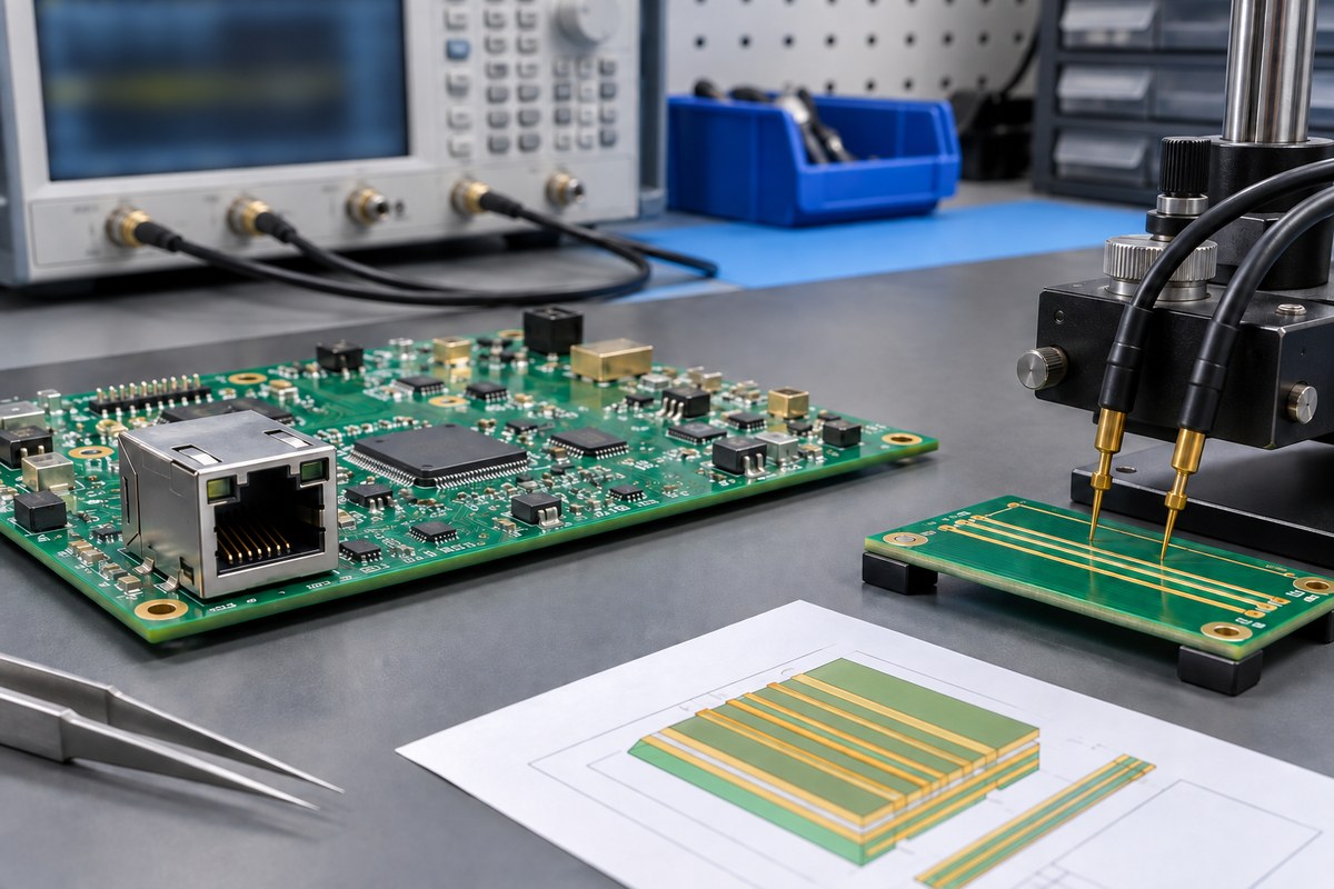
Intended connection: Two points on the same net should normally show a low and stable resistance when no series component is expected between them. Compare the result with the measured lead baseline and repeat from a second accessible point before accepting the route.
Open path: A trace crack, lifted pad, unseated connector, broken via, damaged cable, or unsoldered joint may produce OL, an unexpectedly high resistance, or a reading that changes with permitted movement. Divide the route into sections to separate a real break from poor probe contact.
Unintended connection: Nets that should be isolated may show low resistance because of a solder bridge, conductive debris, moisture, contamination, or internal damage. Confirm the schematic relationship and isolate approved branches before deciding that the low reading is a physical short.
Component path: Windings, fuses, shunts, inductors, transformers, switches, and low-value resistors can legitimately trigger the tone. Identify every component between the probes and measure the numerical resistance or polarity behavior instead of judging the path by sound alone.
The most useful result is therefore not ābeepā or āno beep.ā It is a documented comparison between the measured endpoints, the expected circuit relationship, the measured resistance, and the conditions under which the reading was taken.
What Should You Check Before Testing PCB Continuity?
Prepare the board, meter, and test plan before touching the probes to the PCB. These checks prevent meter damage, false readings, accidental shorts, and unnecessary rework:
Remove and verify power: Disconnect every external supply, powered cable, and battery. Use voltage mode to confirm that the selected points are not energized before switching to continuity or resistance mode. The Fluke continuity testing guide likewise requires a de-energized circuit.
Control stored energy: Discharge capacitors only by the product’s approved service method, then recheck the relevant rails. Do not assume that unplugging the unit removes stored voltage.
Define the expected relationship: Use the schematic, netlist, layout, connector pinout, and board revision to identify both test points and decide whether they should be connected, isolated, or linked through a component.
Establish the meter baseline: Confirm the correct lead terminals and continuity function. Touch the probe tips together and record the lead resistance and audible response, then separate them and verify the open indication.
Choose safe access points: Use fine, insulated probes on test pads, component pads, vias, or connector pins without bridging adjacent conductors. Support the PCB so probe force does not flex it.
Record the board state: Note connected cables, switch positions, installed modules, and any isolated branches. Change one condition at a time and record it so an apparent fault can be reproduced and the board can be restored correctly.
How Do You Perform a PCB Continuity Test with a Multimeter?
Test one defined electrical relationship at a time. The sequence below preserves the original board condition, establishes a meter baseline, and records the resistance needed to distinguish an intended connection from a false short or an open path.
Step 1: Identify the two test points. Mark both endpoints and state whether they should be connected or isolated. Note any resistor, coil, connector, switch, jumper, or protection device between them.
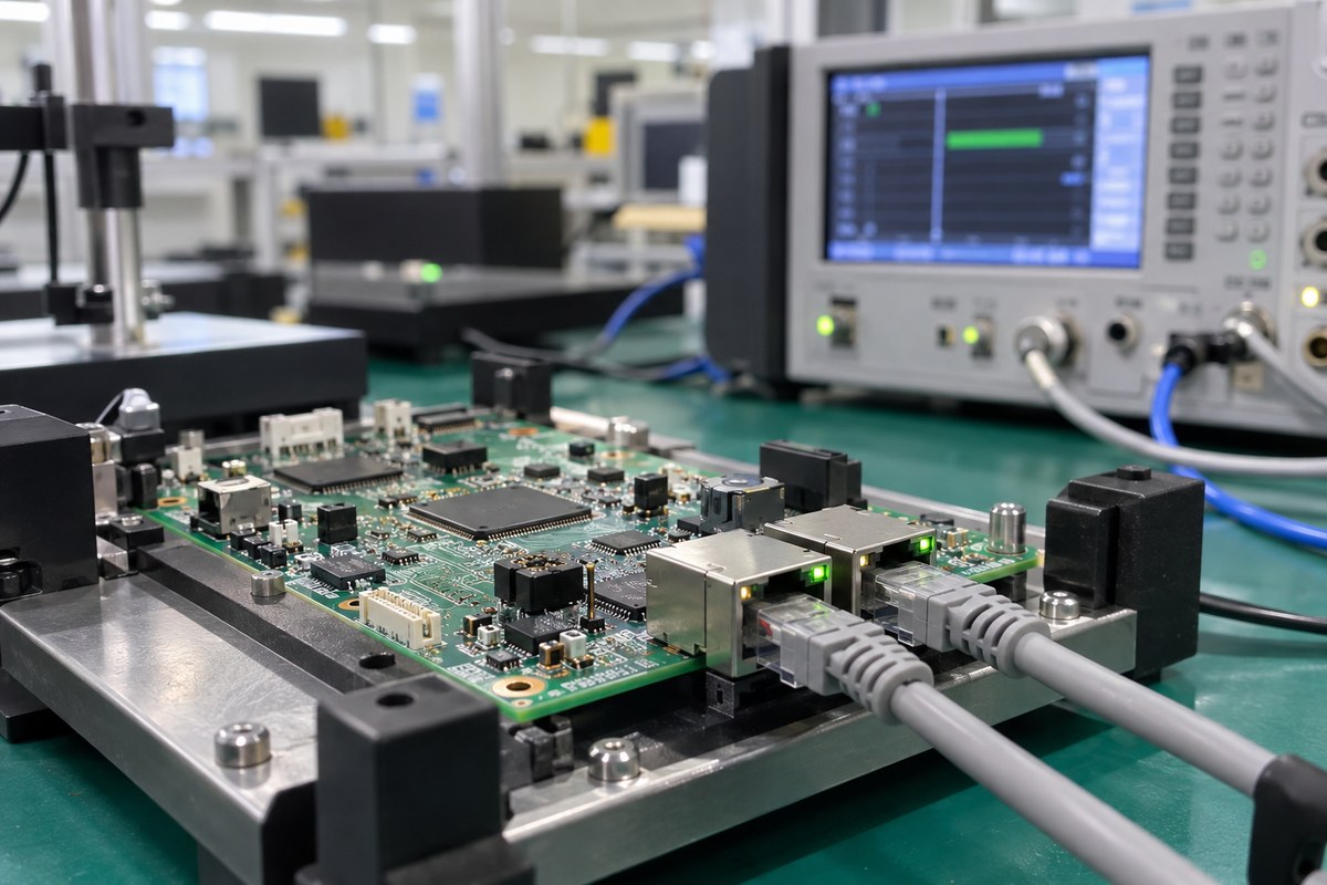
Step 2: Remove power and stored energy. Disconnect supplies and batteries, follow the approved discharge method, and verify the absence of voltage at the relevant rails.
Step 3: Select continuity mode. Place the leads in the correct terminals and select the continuity function. If the meter combines several functions, confirm that the continuity symbol is active.
Step 4: Verify the probes. Touch the tips together and note the lead resistance and tone, then separate them and confirm the open indication.
Step 5: Place the probes on the intended points. Contact exposed test points, pads, terminals, or connector pins without touching neighboring conductors. Do not scrape solder mask merely to create access.
Step 6: Read the resistance and audible indication. Hold both tips steady and note the displayed value, tone, stability over time, board state, and any isolated branches.
Step 7: Compare the result with the design. If it disagrees with the expected net relationship, retest from a second accessible point before rework. One poor probe contact can imitate an open.
Continuity mode is suitable for a connection or isolation question on an unpowered circuit. It does not verify a powered signal, controlled impedance, insulation resistance at a specified voltage, or operation under load.
How Should You Interpret PCB Continuity Test Results?
The displayed resistance has more diagnostic value than the tone alone. Compare the reading with the meter’s lead resistance, the circuit’s expected series elements, and the behavior of a known-good board when one is available.
Observed Meter Behavior
Decision It Supports
Next Verification
Stable reading close to the measured lead resistance on two points of the same net
The accessible path is probably continuous, provided no series component should add resistance
Subtract or account for the lead baseline, then repeat from a second accessible point across the same section
Stable low resistance between nets that the schematic shows as isolated
A real circuit path, parallel component, contamination path, or unintended short may connect the nets
Read the numerical resistance, compare with a known-good board, and isolate approved branches one at a time before rework
OL or a stable high reading between endpoints that should share one net
The route may be open, but poor probe contact, an open switch, or an unexpected series element can give the same result
Recheck the probe baseline and endpoint contact, then divide the route into smaller test sections
Brief tone or resistance that rises and then settles
The meter may be charging capacitance rather than detecting a persistent short
Keep the probes stationary, observe the settled value and repeat after discharge under the approved procedure
Reading changes when probe pressure, connector position, or permitted board support changes
An intermittent contact, cracked trace, via barrel, solder joint, connector, or unstable probe contact is possible
Immobilize the probes, repeat the test, and inspect the smallest affected section under magnification
A short tone that stops can be normal when a capacitor initially charges through the meter. A persistent low reading between supply and ground may still be normal for a low-voltage, high-current circuit. Use the schematic and expected resistance rather than a universal pass threshold.
How Do You Find an Open Circuit or Broken PCB Trace?
Localize an open by testing progressively smaller sections of the intended net:
Confirm the expected route. Use the schematic and PCB layout to identify the two endpoints, intermediate pads, vias, connectors, jumpers, and any legitimate series components.
Verify the meter and contacts. Recheck the probe baseline, then confirm solid contact on known-good exposed points before treating an OL indication as a board fault.
Test the complete path. Measure between the two endpoints and record the numerical resistance, audible indication, board state, and probe locations.
Divide the route into sections. Keep one probe on a known-good endpoint and test a midpoint. Continue in the failed half until the open is bounded between the last passing point and the first failing point.
Use existing access points. Probe test pads, component pads, connector pins, or exposed vias shown on the layout. Do not scrape solder mask merely to create access.
Confirm before rework. Repeat from a second pair of points and inspect the isolated section under magnification. Use X-ray when the suspected joint or transition is hidden.
If the reading changes while the board is gently supported, suspect an intermittent trace, via barrel, solder joint, or connector contact. Apply movement only when the diagnostic procedure permits it, and never cut a trace, remove a component, or expose copper until the fault is reproduced and confirmed.
How Do You Check a PCB for an Unintended Short Circuit?
Start with two nets that the schematic says must be isolated. Disconnect external cables, compare the measured resistance with a known-good board of the same revision when available, and then isolate branches in a controlled sequence. The suspect area is the portion that remains connected after unrelated branches are removed.
Inspect first: Look under magnification for solder bridges, conductive debris, damaged insulation, misaligned parts, and residue between adjacent pins. Map each visible suspect to the two measured nets so cosmetic residue is not mistaken for the electrical cause.
Measure in resistance mode: Record the numerical value, probe polarity, and whether the reading rises, falls, or remains stable. A brief tone followed by increasing resistance suggests different behavior from a persistent value near the lead baseline.
Separate branches: Disconnect external loads, connectors, or approved jumpers one at a time and retest after each controlled change. Record the original state and every removal so the branch that changes the reading can be identified and restored correctly.
Compare locations: Probe multiple accessible points along both suspected nets to determine whether the low reading is local or present across the full network. A board-wide value may reflect a legitimate shared load; a change across one short section narrows the physical search.
Continuity locates an electrical relationship, not the physical defect by itself. Thermal methods, current-limited power injection, or component removal require a controlled repair procedure and are not substitutes for first confirming the unpowered resistance path.
Why Can a PCB Show Continuity When There Is No Short Circuit?
A continuity tone means the meter sees resistance below its audible threshold. It does not mean the path is zero ohms or that the board contains a short. The threshold, response speed, and test current vary by meter, so two instruments can behave differently on the same PCB.
Power and ground may beep because the circuit includes low-value loads, shunts, transformer windings, protection devices, or several parallel branches. Capacitors can also produce a brief tone while they charge from the meter. If the displayed resistance rises, the response is not the same as a stable metallic short.
Switch to resistance mode, observe the value over time, reverse the probes when semiconductor junctions may be involved, and compare the result with the schematic. A persistent low reading deserves investigation, but it must be judged against the design’s expected unpowered resistance. There is no universal resistance value that proves every PCB power rail is shorted.
An assembled circuit often contains several paths between the probe points. Treating it like a single copper trace creates false short and false open diagnoses.
Capacitors: A discharged capacitor can produce a brief tone or low initial resistance that rises as it charges from the meter. Hold the probes steady and judge the settled value and repeatability instead of classifying the first beep as a short.
Diodes and semiconductor junctions: A junction may conduct in one probe direction and block in the other, so continuity results can change when the leads are reversed. Compare both polarities and use diode mode when the schematic shows a semiconductor in the measured path.
Inductors, fuses, shunts, and windings: These parts can be legitimate low-resistance series paths that trigger the tone. Confirm the component identity and expected resistance, then measure across the part and the surrounding copper separately to distinguish an open element from an open trace.
Pull resistors and parallel networks: Parallel components can connect the endpoints through another branch even when the specific trace under test is open. Isolate an approved branch or move the probes to points that place only the target segment between them.
Switches and connectors: The measured network changes with switch position, connector engagement, oxidation, and contact movement. Record the exact mechanical state and repeat the test without moving the probes before calling a changing value intermittent.
Conformal coating and residue: Coating can prevent reliable metal contact, while conductive contamination can create a leakage path that looks like partial continuity. Use designated exposed test points, inspect the contact area, and clean only under an approved process before retesting.
When the reading is ambiguous, record it in resistance mode, reverse the probes, disconnect one approved branch at a time, and compare the time behavior. Those observations distinguish a fixed copper connection from a component-dependent path.
How Do You Test PCB Vias, Solder Joints, Connectors and Ground Connections?
Choose endpoints that place the feature itself in the measured path. A normal result means the connection matches the schematic and is close to the lead-resistance baseline when no intentional series element is present; an open, unstable, or unexpectedly low reading requires a nearer comparison point.
PCB trace: Probe exposed nodes at both ends of the trace. A stable reading near the lead baseline is expected for a direct copper path; OL or instability points to a break, damaged pad, or poor contact.
Via: Measure from an exposed pad before the layer transition to the nearest accessible point after it. An open result can indicate a cracked barrel or internal connection, although surface probing cannot show the exact internal failure location.
Solder joint: Probe the component lead and the next copper node, not two points on the same solder fillet. A changing or high reading can indicate incomplete wetting, a crack, or a lifted pad.
Connector: Test from the board-side net to the mating contact. The result should remain stable through the permitted engagement check; changes can indicate oxidation, weak contact force, or a damaged termination.
Fuse: Probe one terminal on each side of the isolated fuse. A good low-resistance fuse should read near the lead baseline; OL indicates an open element or poor terminal contact.
Ground connection: Confirm that both points belong to the same ground net before expecting continuity. Chassis, analog, digital, isolated, and filtered grounds may connect through controlled elements or remain separate.
Repeat an unexpected result from a second accessible point and inspect the feature before rework. Probe pressure can temporarily close a cracked joint or move a connector contact, producing a misleading pass.
How Is Continuity Testing Different on a Bare PCB and an Assembled PCBA?
An unpopulated PCB can be compared directly with its netlist because components do not create alternate paths. An assembled PCBA contains resistors, capacitors, inductors, semiconductors, connectors, and powered subsystems, so the same two test points may produce a legitimate reading that would look like a short on a bare board.
Bare PCB objective: Verify that every required network is continuous and that separate networks remain isolated according to the released design data. A failure points toward copper, via, pad, or fabrication-data issues because installed components are not yet creating alternate paths.
Assembled PCBA objective: Investigate one defined circuit relationship while accounting for components, jumpers, switches, connectors, and attached equipment. Before judging the reading, identify which installed paths can legitimately connect the selected points.
Test coverage: A production bare-board program can check a controlled set of nets and isolation relationships systematically. A handheld PCBA check samples only the points chosen by the technician, so an untested branch cannot be called good from one passing pair.
Acceptance basis: Bare-board acceptance can be tied to the released netlist and agreed electrical-test requirements. PCBA troubleshooting also needs the schematic, board state, component behavior, expected resistance or polarity, and a repeatable record of what was disconnected.
A bare-board pass does not prove assembly workmanship, component value, firmware operation, signal quality, or performance under load. Conversely, an unexpected assembled-board continuity reading does not prove that the bare PCB contains a fabrication defect.
When Is a Multimeter Continuity Test Not Enough?
A handheld meter is suitable for a small number of known points, but it does not provide complete network coverage or prove performance outside its low-energy resistance check. Escalate the test method when the decision depends on one of the following:
High net count: Manually probing a few pairs cannot demonstrate systematic coverage on a dense board. Use a controlled test program derived from the released design data and retain the tested-net and exception record.
Hidden structures: Surface probes cannot identify the physical condition of internal traces, buried vias, or bottom-terminated solder joints. Combine electrical localization with X-ray, cross-sectioning, or another inspection method selected for the suspected structure.
Insulation requirements: A continuity function uses low test energy and cannot establish leakage or dielectric withstand at a specified voltage. Use the applicable insulation-resistance or high-potential method with defined limits and safety controls.
Current-carrying risk: A thin or partially cracked conductor may pass the meter’s low-current check but develop excessive voltage drop or heating in service. Escalate to an approved resistance, voltage-drop, or loaded test when current capacity is the decision.
Signal or functional risk: Continuity does not measure impedance, crosstalk, insertion loss, timing, firmware operation, component value, or performance under load. Use the powered functional or signal-integrity test that corresponds to the actual failure symptom.
Intermittent reliability: A connection that passes at rest may fail only during thermal change, vibration, permitted flexure, or connector use. Reproduce the defined condition while monitoring the circuit with suitable logging instead of relying on a single static reading.
Choose the next method from the failure risk: resistance or diode mode for component-dependent readings, X-ray for hidden joints, insulation testing for leakage risk, powered measurements for operating behavior, and functional test for system outputs. Record the board revision, test points, circuit state, instrument, displayed value, and disposition so another technician can repeat the decision.
How Are PCB Opens and Shorts Tested During Manufacturing?
Production electrical testing compares the unpopulated board’s conductive networks with released design data. It checks required connections for opens and separate networks for unintended shorts under the agreed test conditions. The method is selected according to quantity, board access, program data, fixture economics, and reporting requirements.
Flying-probe test: Movable probes contact programmed pads without a dedicated bed-of-nails fixture, making program changes easier for prototypes and changing revisions. The quotation and test plan should state accessible-point limitations, expected coverage, program revision, and whether opens and shorts are both included.
Fixture-based test: A dedicated fixture can contact many points simultaneously and shorten repeated test cycles after the design stabilizes. Before committing to it, confirm test-pad access, fixture ownership, maintenance, revision-change cost, and how engineering changes invalidate the fixture or program.
Netlist control: The test program must represent the released board revision and the intended net relationships after any approved data transformation. Verify the source files, revision identifier, exclusions, and engineering-change linkage; a perfectly executed obsolete program can approve the wrong board.
Result traceability: The retained record should identify the board or lot, program and design-data revisions, method, tested scope, pass/fail result, exceptions, retest disposition, and report-retention requirement. These fields let quality teams distinguish a real repeat failure from a changed design or test program.
Flying-probe testing often suits prototypes and changing revisions because it avoids a dedicated fixture. Stable mass-production volumes may justify a bed-of-nails fixture for shorter repeated test cycles. The choice does not change the acceptance basis: both methods need controlled netlist data, defined continuity and isolation criteria, and traceable results.
The scope of IPC-9252B electrical testing requirements addresses conductive networks on unpopulated printed boards. Electrical test does not replace dimensional and solder-mask inspection, assembly inspection, or functional testing.
A repeatable PCB continuity test record should identify the drawing, schematic, or netlist revision used for interpretation. Purchase documents should also state the governing requirement, supplied test data, reporting format, and project-specific limits.
FAQs About PCB Continuity Testing
Q1: Can I test PCB continuity with the power on?
A1: No. Continuity and resistance modes apply their own test stimulus, so external voltage can corrupt the reading and may damage the meter or board. Remove all power and verify the absence of voltage first.
Q2: What resistance should a good PCB trace have?
A2: A short direct copper path normally reads close to the meter’s lead resistance, but there is no universal value for every trace. Length, width, copper thickness, connectors, and intentional series elements affect the result.
Q3: Does a beep always mean continuity?
A3: It means the measured resistance is below that meter’s audible threshold. The path may be an intended trace, a component, a parallel branch, or an unintended connection, so the schematic determines its significance.
Q4: Why does my PCB beep between power and ground?
A4: Low-resistance loads, shunts, transformer windings, protection devices, parallel paths, or charging capacitors can connect the rails in an unpowered circuit. Read the resistance over time and compare it with the design before diagnosing a short.
Q5: Can a capacitor cause a continuity beep?
A5: Yes. The meter may briefly charge the capacitor, creating a tone or low initial resistance that rises. A stable low reading has a different diagnostic meaning.
Q6: Can a multimeter detect a broken via?
A6: It can show that the path across a via transition is open or unstable when accessible points exist on both sides. It cannot identify the precise internal crack location without layout data and additional inspection.
Q7: Does probe polarity affect continuity testing?
A7: It can on an assembled PCBA. Diodes, transistor junctions, and IC protection structures may conduct differently when the probes are reversed; diode mode can clarify the path.
Q8: Can continuity testing damage components?
A8: An energized circuit or an unsuitable meter test condition can create risk. Remove power, follow the component or product service guidance, and avoid probing modes that exceed the permitted terminal conditions.
Q9: Why does the continuity reading keep changing?
A9: Capacitor charging, unstable probe contact, connector movement, contamination, or an intermittent crack can change the effective path. Hold the probes steady, observe the time pattern, and isolate branches before assigning the fault.
Q10: Can a PCB pass continuity testing but still fail?
A10: Yes. A low-current path can pass while the board still has impedance, insulation, component, firmware, signal-integrity, current-capacity, or functional defects that continuity mode cannot evaluate.
A PCB continuity test is reliable when the circuit is unpowered, the expected net relationship is known, the meter and leads are checked, and the result is interpreted from resistance rather than a beep alone. Parallel paths, capacitors, semiconductors, contact quality, and mechanical movement must be considered before an open or short is assigned to the board.
If production continuity, isolation, or PCBA test coverage must be quoted, send the released Gerber or ODB++ data, netlist, BOM, quantity, test limits, and report requirements to sales@bestpcbs.com. EBest Circuit can review whether the requested scope belongs to bare-board electrical testing, assembly inspection, or project-specific functional testing.
PCB panelization arranges multiple circuit boards within one manufacturing panel so fabrication, solder paste printing, placement, reflow, inspection and handling can process them as a stable unit. A useful panel is not simply the layout that fits the most boards. Its outline, rails, spacing, separation method, tooling features and component clearances must match the fabricator’s CAM rules, the assembly line and the final depaneling process.
What Is PCB Panelization?
PCB panelization converts one PCB design, or a controlled set of compatible designs, into a larger array that production equipment can transport and process. The finished panel normally includes the repeated board images, panel rails, separation features, global fiducials, tooling holes and identification marks. After assembly and testing, the individual boards are separated by V-scoring, routing, punching, sawing or laser cutting as appropriate.
A single PCB may be large and rigid enough to run without a delivery array, but small, narrow, irregular or thin boards often need added support. The phrase panelization construction is sometimes used for the complete arrangement of boards and temporary panel features. Practical PCB panelization guidelines must therefore define both the customer delivery panel and the fabricator-controlled production panel, which may include several delivery panels plus test coupons.
Why Is Panelizing PCB Important for Fabrication and SMT Assembly?
Panelizing PCB designs reduces repeated handling and gives conveyors, printers, placement machines and inspection systems a consistent rectangular workpiece. Several boards can pass through one stencil print, one placement program and one reflow cycle. Panel rails also protect edge components and create room for machine references that would not fit on a small finished board.
The benefit depends on the whole route. A dense array can improve laminate utilization but become too flexible under stencil pressure. A rigid array may process well yet waste material or impose excessive stress during separation. When the same supplier controls FR4 PCB fabrication and PCB assembly, CAM and SMT engineers can review the delivery panel against fabrication tolerances, stencil data, component placement and depaneling access before release.
Which PCB Panelization Methods Should You Choose?
The separation method should be chosen before the array geometry is frozen. The main PCB panelization methods have different shape, spacing, stress and edge-finish limits.
V-scoring: uses straight grooves from opposite sides of the panel. It is space-efficient for rectangular boards with continuous straight separation lines.
Tab routing: routes most of the board outline while leaving solid tabs. It supports irregular contours and allows the tabs to be cut by a router.
Mouse bites: add perforated holes to breakaway tabs for manual separation. A PCB panelization mouse bites pattern must match the fabricator’s drill and routing capabilities.
Laser depaneling: provides a narrow, non-contact cut path for suitable materials and thicknesses, but it needs specialized equipment and process review.
Punching or sawing: can suit stable high-volume geometries, although tooling cost or straight-line limits restrict their use.
The manufacturer should confirm channel width, residual web, tab placement and keepouts rather than relying on a universal online drawing. Material, finished thickness, copper distribution and component layout all change the result.
How Do V-Score and Tab Routing Compare?
The decision starts with board geometry and permitted separation stress. V-score favors straight outlines and high panel utilization. Tab routing accepts complex shapes and controlled tab locations but consumes area for the router path.
Decision factor
V-score
Tab routing / mouse bites
Board outline
Straight, continuous separation lines
Curved or irregular outlines are possible
Board spacing
Boards may share a score line
Routing channel is required
Separation stress
Can flex a longer board edge
Localized at selected tabs
Finished edge
Straight scored edge
Tab witness may remain unless machine-routed flush
Component placement
Needs clearance from the score and flex zone
Needs clearance from tabs, router access and breakout force
Best fit
Rectangular, repeatable arrays
Irregular shapes and selective support points
For more detail on breakout geometry, see the related guides to mouse bites versus V-groove and V-cut PCB depaneling. The production drawing should still use the dimensions approved for the current manufacturer and equipment.
What Panel Rails, Fiducials and Tooling Holes Are Required?
Panel rails create straight conveyor edges, increase stiffness and hold temporary production features. Their width follows the printer, conveyor, fixture and depaneling setup, not a fixed internet value. Rails may also carry global fiducials, tooling holes, barcodes, coupons and orientation marks.
Global fiducials establish panel translation and rotation for vision-guided equipment. An asymmetric arrangement reduces the chance of loading the panel in the wrong orientation. Tooling holes provide mechanical registration where a fixture or process requires it. Local board fiducials may still be needed near fine-pitch BGA, QFN or other placement-critical packages.
The panel data used to manufacture an SMT stencil must use the same board step-and-repeat, origin and orientation as the placement data. A stencil generated from a single-board paste layer cannot be assumed to match a later CAM-created array unless the duplication and datum transformation are controlled.
How Should PCB Panel Size, Spacing and Component Clearance Be Set?
A reliable PCB panel design starts with the usable machine envelope, then reserves rails, separation geometry and component keepouts before calculating the array count. Filling the entire fabrication sheet first can produce a panel that cannot be printed, transported or depanelized safely.
PCB panel size is constrained by every machine that must handle the panel, including fabrication equipment, stencil printers, pick-and-place systems, reflow conveyors, AOI, test fixtures and depaneling equipment. The smallest and largest usable dimensions, conveyor direction and rail requirements should be confirmed with the actual production route.
Board-to-board spacing follows the separation tool. V-score can place straight board edges together, while routing needs a channel wide enough for the selected cutter and positional tolerance. Laser separation may use a narrower path but requires material and thermal-process review. A PCB panelization calculator can estimate how many boards fit, but it cannot see every process restriction or guarantee the lowest finished-board cost.
Component clearance must include the body, solder joints, overhang, tool envelope and expected board flex. Ceramic capacitors, BGA corners, connectors and heavy parts close to a break line deserve particular attention because depaneling strain can damage a solder joint without leaving an obvious board crack. Copper, vias and controlled-impedance structures also need clearance from score grooves, routed channels and mouse-bite holes.
When Can Different PCBs Share One Panel?
Different PCB part numbers can share a panel only when their fabrication and assembly requirements are compatible. A mixed array generally needs the same material system, layer stack, finished thickness, copper weight, surface finish, solder mask process and production quantity ratio. If one design changes, the shared panel and its assembly data may also require revision.
A homogeneous panel containing one repeated design is easier to control, inspect and replenish. A heterogeneous panel can synchronize a product set and improve material utilization, but it may create unwanted inventory if the demand ratio changes. Rotated boards can improve nesting, yet their copper distribution and component orientation should be checked for reflow, wave soldering and inspection consistency.
Rigid-flex PCB and flex PCB panelization need additional attention to stiffeners, coverlay, bend regions, tooling support and final separation. Their temporary support strategy should be reviewed as part of the material and assembly process rather than copied from a rigid FR4 grid.
What Files Define the Panelization of PCB Arrays?
The panelization of PCB arrays should be defined by one controlled data package. At minimum, identify the finished panel outline, board origins, step-and-repeat, routing or scoring paths, tabs, fiducials, tooling holes, rails and critical dimensions. The fabrication data and the drawing must agree.
Gerber or ODB++: copper, mask, legend, profile and panel-level production features.
NC drill and rout files: tooling holes, mouse bites, slots and routed channels.
Pick-and-place data: component coordinates transformed to the panel origin and repeated orientation.
Paste and stencil data: the same array count and datum used by assembly.
Assembly drawing: panel orientation, board references, special handling and depaneling restrictions.
Do not submit a customer-created panel Gerber together with a single-board NC drill or placement file unless the relationship is explicitly controlled. Mismatched repetition counts, origins and rotations are a common source of preventable CAM and assembly questions.
Which PCB Panelization Software and Tools Are Useful?
A PCB panelization tool is useful for layout exploration, but the correct choice depends on who owns the production data. PCB panelization software inside ECAD can preserve design links; CAM software can duplicate manufacturing layers, drill data and net information; a PCB panelization calculator is best treated as an early utilization estimate.
PCB panelization Altium workflows: Embedded Board Array and Draftsman can create repeated arrays and fabrication drawings. Searches for Altium PCB panelization and Altium Designer PCB panelization normally refer to these functions.
PCB panelization KiCad workflows: plugins or hierarchical layout methods can create arrays, but users should verify Gerber, drill, position and reference-designator output. The phrase KiCad PCB panelization describes the same task from the tool-first search direction.
Fusion 360 PCB panelization: users should confirm whether the selected Electronics/EAGLE workflow exports every required manufacturing and assembly layer for the array.
Free PCB panelization software: may be adequate for geometry trials, but output integrity, drill duplication, netlist consistency and revision control still require checking.
Manufacturer CAM: usually offers the strongest alignment with actual material utilization, routing tools, panel borders and production equipment.
Software does not know every shop-specific limit. The released files should be checked in an independent CAM viewer and approved against the manufacturer’s panel drawing.
Should You Panelize the PCB or Let the Manufacturer Do It?
Let the manufacturer create the panel when the main goal is cost-efficient fabrication and the array has no product-specific mechanical constraints. Supply clean single-board data, state whether boards must arrive as a panel or separated, identify the assembly route and approve the returned panel drawing. This lets CAM use current working-panel sizes, routing tools and process margins.
Create and control the panel yourself when the assembly fixture, test nest, barcode position, mixed-design ratio, break sequence or customer equipment requires an exact delivery format. In that case, provide both the panel data and the original single-board source, then allow a DFM review. Ownership of the layout does not remove the manufacturer’s responsibility to flag incompatible geometry.
EBest Circuit (Best Technology) lists PCB dimensions up to 610 x 610 mm, subject to stack-up, material, panel utilization and engineering review. The published PCBA process includes 3D SPI, AOI, X-ray and functional testing. Those capabilities are useful only when the approved panel, stencil, placement data and inspection program share the same revision and datum.
How Does PCB Panelization Affect Cost and Yield?
Panelization changes cost through laminate utilization, machine handling, tooling, assembly cycle time, inspection and depaneling. Increasing the number of boards per panel can reduce handling per board, but a weak or warped array can increase paste defects, placement error or breakage. The lowest material scrap is not always the lowest total cost.
Compare layouts using finished good boards per panel, expected yield and all required operations. Include routing time, score setup, tab finishing, carrier or fixture needs, stencil size, test access and the labor or machine time required to separate boards. A mixed array can reduce material waste while increasing data control and inventory risk.
What Must Be Checked Before a PCB Panel Is Approved?
Approval should freeze the panel revision that fabrication, stencil, placement, inspection and test will use. Review the panel drawing and rendered CAM output together rather than approving a dimension table in isolation.
Overall panel dimensions, thickness, quantity per panel and conveyor direction are stated.
V-score, routing channels, tabs and mouse bites match the intended depaneling process.
Rails, fiducials, tooling holes and orientation marks match SMT equipment and fixtures.
Components, copper and vias have adequate clearance from every separation feature.
Gerber/ODB++, NC drill, stencil, placement and assembly drawings use the same origin, rotation and revision.
The panel remains sufficiently rigid through printing, placement, reflow, inspection and handling.
Mixed designs share compatible stack-up, materials, finish and production ratio.
First-panel separation verifies edge quality, strain-sensitive components and fixture access before volume release.
The related PCB panelization approval guide provides a focused release-control workflow. For the present project, keep the signed panel drawing with the manufacturing package so later revisions cannot silently change the array.
PCB Panelization FAQ
What Is Meant by PCB Panelization?
What is meant by PCB panelization is the temporary grouping of multiple boards into one production unit. The boards remain connected during fabrication or assembly and are separated after the required processes are complete.
Does Every Single PCB Need a Panel?
No. A sufficiently large, rigid and machine-compatible single PCB may run without a delivery array. Small, irregular, thin or edge-sensitive boards usually benefit more from rails and repeated panel processing.
Can a PCB Panelization Calculator Produce Final Manufacturing Data?
It can estimate board count and utilization, but final data still needs routing, score, rail, tooling, fixture and equipment review. Treat the result as a layout proposal rather than automatic production approval.
Can Flex PCB Panelization Use the Same Rules as Rigid FR4?
Not automatically. Flex PCB panelization may use stiffeners, temporary carriers, tooling strips or material-specific separation methods. Bend regions, coverlay and thin-material handling require process-specific review.
Can the PCB Manufacturer Panelize Single-Board Gerbers?
Yes, and this is often the simplest route when the delivery panel has no fixed fixture constraints. State the required panel delivery, assembly process and depaneling preference, then approve the manufacturer’s drawing before production.
Conclusion
Effective PCB panelization connects board geometry with fabrication, SMT handling, separation and data control. Choose the depaneling method first, define rails and machine references, keep every production file on one datum and approve the rendered panel before release. For a DFM review of single-board or controlled panel data, contact EBest Circuit (Best Technology) at sales@bestpcbs.com.
Choosing among HDI PCB manufacturers in UK requires more than finding a supplier that lists āHDIā on a capability page. The right manufacturer must review your actual buildup, explain how each microvia is formed and filled, identify the proposed production site, and show how the released construction will be controlled from prototype through repeat orders.
Start with the features that create manufacturing risk: microvia layer pairs, stacked or staggered structures, via-in-pad, lamination cycles, finished copper, fine features, material system and impedance requirements. Then compare suppliers using the same files, quantities, inspection scope and delivery assumptions. This exposes incomplete quotations early and turns a general supplier search into a defensible manufacturing decision.
How to Choose an HDI PCB Manufacturer in UK?
Choose an HDI PCB manufacturer in UK by matching the proposed factory, process controls and evidence package to your board. A UK address may represent a fabrication site, sales office, managed supply service or assembly provider, so the quotation should name where the bare board will be produced and which operations are subcontracted.
Match the buildup: submit the layer stack and microvia start/stop layers so the supplier cannot silently simplify the routing concept.
Confirm materials: identify the laminate family, electrical properties and acceptable substitutions because changes can alter impedance and pressing behavior.
Check prototype and production routes: ask whether both use the same site, materials and critical processes; define approval for any transfer.
Agree on evidence: specify electrical test, microsection, impedance verification, inspection reports and lot records before comparing prices.
Evaluate assembly ownership: for BGA, CSP or via-in-pad designs, determine how bare-board findings return to the assembly team.
Judge communication by output: a useful supplier returns a marked-up stackup, DFM questions, deviations and an evidence planānot only a quick reply.
What Capabilities Should HDI PCB Manufacturers in UK Provide?
Look for capabilities that correspond directly to routing, component, signal-integrity and reliability requirements. Minimums depend on layer count, copper weight, material, panel size and volume.
HDI process capability
Published UK capability example
Maximum layer count
Up to 32 layers
Laser microvia diameter
Down to 75 µm
Mechanical drill diameter
Down to 0.105 mm
Fine track and gap
Down to 50 µm
Microvia aspect ratio
Up to 1:1
Sequential lamination
Up to 6 lamination cycles
Supported via structures
Blind, buried, stacked and staggered microvias
Via filling
Copper-filled and resin-filled vias
Controlled impedance
±10% standard; ±5% advanced capability
Electrical test
100% electrical test
The numerical examples above are currently published by Exception PCB for its UK HDI production environment; Rush PCB UK separately publishes up to 20+ layers, 0.1 mm microvias and 50/50 µm trace/space. These are screening references, not universal limits for all HDI PCB manufacturers in UK. Require the shortlisted factory to return values tied to your material, copper, panel and volume.
How Can You Verify a Reliable HDI PCB Manufacturer in UK?
A reliable manufacturer connects each important claim to a site-specific process, review record and acceptance method. Certificates may support qualification, but they do not prove that a particular microvia stack has been assessed.
Build-specific DFM: require comments tied to actual layer pairs, microvia spans, copper, materials and tolerances. A generic āapprovedā response does not show that the construction was reviewed.
Named production site: record the physical factory and which processes it performs. If laser drilling, filling or testing is subcontracted, require the responsible site and control method.
Material traceability: record manufacturer, grade and lot identity, and require approval before substitution. This protects impedance and lamination behavior from unreviewed changes.
Microvia evidence: agree on microsection locations, plating and fill criteria, sampling frequency and the report supplied with the order.
Electrical and impedance testing: define the source netlist, test coverage, coupon design, target tolerance and report format rather than accepting ātestedā as a complete answer.
Registration control: ask how sequential-lamination registration is monitored and what evidence demonstrates that capture pads and interlayer alignment meet the drawing.
Prototype-to-production consistency: confirm whether the same stackup, material, factory and critical process route will be used after prototype approval.
Change and nonconformance control: define which changes need written approval and who owns containment, root-cause analysis and corrective action after fabrication or assembly.
Request report samples before ordering. This proves the evidence is part of the operating process rather than a document requested after the boards are finished.
Why Choose EBest as an Alternative to HDI PCB Manufacturers in UK?
When UK production is not a contractual requirement, EBest Circuit offers a China-based route that connects HDI fabrication, engineering review and PCB assembly. EBest is not presented as a UK manufacturer; it is an alternative for UK projects needing coordinated overseas manufacturing.
Build-specific review: stackup, microvia map, via-in-pad, materials and impedance are reviewed against the intended construction.
DFM before production: Gerber or ODB++, drill data and notes are checked for ambiguous transitions, conflicts and avoidable complexity.
Fabrication and assembly coordination: board production, sourcing, SMT, inspection and test can share one project workflow.
Prototype-to-volume control: approved data, revisions and deviations can be retained for later builds.
Project-defined evidence: electrical test, AOI, microsection, impedance and assembly inspection are scoped to the design.
Pre-quotation support: unresolved manufacturing and assembly questions are identified before commercial comparison.
Send Gerber or ODB++, stackup, drill files and project requirements to sales@bestpcbs.com for a free DFM review and quotation.
How Should You Compare Quotes From HDI PCB Manufacturers in UK?
Compare quotations only after every HDI PCB manufacturer in UK has priced the same construction, production route and acceptance evidence. Use the following checks:
Freeze the technical baseline: use one released stackup, via map, material requirement, copper weight, surface finish and impedance table. Otherwise, a lower quote may represent a simpler board.
Separate setup from unit price: identify tooling, engineering, coupons and one-time test charges so repeat-order cost is visible.
Confirm the buildup assumption: require the quoted lamination cycles and stacked/staggered microvia treatment in writing because they are major cost drivers.
Check included evidence: state whether electrical test, impedance reports, microsections, first-article records and certificates are included or charged separately.
Identify the production site: compare UK-built, UK-managed and overseas manufacture honestly; include freight, import handling and any transfer risk.
Normalize quantity and delivery: request the same prototype, pilot and repeat-order quantities with the same delivery point and required date.
List every deviation: a quote that substitutes material or omits a process is not comparable until the difference is reviewed and accepted.
Which Design Choices Increase Quotes From HDI PCB Manufacturers in UK?
Design choices increase cost when they add process cycles, reduce yield or require tighter verification. DFM can reduce those costs without weakening function.
Extra buildup cycles: each adds pressing, drilling, imaging and registration work.
Stacked microvias: use them for necessary vertical transitions; staggered structures may be simpler when routing permits.
Filled and capped vias: restrict them to locations that require pad escape, thermal or assembly performance.
Fine features: review local bottlenecks instead of applying an extreme rule across the board.
Specialty materials: specify performance needs and permitted alternatives to avoid unnecessary sourcing constraints.
Inspection: connect each extra record or test to a real risk and acceptance decision.
What Lead Time Should You Expect From an HDI PCB Manufacturer in UK?
Published UK supplier examples place HDI prototypes from about 5 working days, while more complex HDI/BBV builds are commonly presented around 7ā10 working days. Some suppliers advertise 1ā5-day expedited options, but those are conditional services rather than a dependable default for every stackup.
Planning case
Indicative published range
What can extend it
Simple, materials-available HDI prototype
From about 5 working days
Open DFM questions, special material, via filling or added reports
More complex HDI or blind/buried-via build
About 7ā10 working days as a planning reference
Multiple lamination cycles, stacked vias, tight registration or non-stock laminate
Expedited service
Some UK suppliers advertise 1ā5 working days
Available only after design, material, capacity and inspection review
HDI plus assembly
Bare-board lead time plus component and PCBA schedule
Long-lead components, stencil, programming, X-ray or functional testing
The ranges are based on current supplier-published examples: Pure PCB lists HDI prototypes from five working days and an HDI/BBV range of 7ā10 days, while Rush PCB UK advertises conditional 1ā5-day quick-turn options. Treat them as RFQ planning references, not EBest promises or universal UK lead times. Ask the selected manufacturer to return a milestone schedule covering DFM approval, material release, lamination, drilling/filling, inspection, assembly and shipping.
How Should an HDI PCB Manufacturer in UK Select Materials?
An HDI PCB manufacturer in UK should select a material system from the electrical requirement, thermal exposure, lamination sequence, thickness target and supply riskānot from Tg alone.
For standard digital and industrial HDI: confirm that the chosen high-Tg FR-4 supports the required press cycles and finished thickness without uncontrolled material substitution.
For high-speed or RF nets: provide target Dk/Df assumptions, frequency and impedance geometry so the fabricator can model the actual construction.
For repeated reflow or higher thermal demand: review decomposition behavior, z-axis expansion and moisture control together with the assembly profile.
For thin dielectrics and microvias: verify that prepreg and core availability supports the required microvia depth, resin flow and copper distribution.
For procurement continuity: name the preferred grade and approved equivalent criteria; require notification before any change that affects impedance or lamination.
The RFQ should record manufacturer, grade, dielectric construction, copper type and weight, required electrical data, approved alternatives and substitution authority. The reviewed production stackup should be returned before release.
How Should an HDI PCB Manufacturer in UK Control Via-in-Pad?
An HDI PCB manufacturer in UK should control via-in-pad as a complete fill, cap and surface-planarity process. The buyer should verify:
Via geometry: define drill diameter, depth, aspect ratio and connected layers so the fill process is evaluated against the real structure.
Fill and cap: state whether conductive or non-conductive fill is required, the copper-cap expectation and any void acceptance criterion.
Planarity: specify the finished BGA/CSP pad requirement and inspection method because uneven pads can change paste volume and joint formation.
Surface finish: review finish selection and thickness after planarization; the final pad, not the unprocessed via, must meet assembly needs.
Fabrication-to-PCBA feedback: align stencil, reflow and X-ray inspection with pad acceptance so solder defects can be separated from bare-board defects.
Put these requirements in the fabrication drawing and via map. Do not rely on a note that says only āVIPPOā or āvia-in-pad,ā because it does not define the acceptance result.
How Should an HDI PCB Manufacturer in UK Plan Sequential Lamination?
An HDI PCB manufacturer in UK should translate the via map into a documented sequence of core preparation, lamination, laser drilling, filling and inspection.
Map every microvia span: show which vias are formed after each press cycle and where stacked interfaces occur.
Confirm the minimum necessary cycles: extra buildup stages increase alignment work, cost and lead time; remove a cycle when routing permits a simpler transition.
Control materials through repeated pressing: verify dielectric thickness, resin behavior and copper balance for the complete thermal history.
Protect registration: review capture pads, material movement allowances and the evidence used to verify interlayer alignment.
Define stage-specific inspection: identify which structures require microsection or other checks before later layers make them inaccessible.
Freeze the production stackup: require approval before changing layer sequence, material, site or via structure after prototype acceptance.
What Files Should You Send to an HDI PCB Manufacturer in UK?
A useful quote needs enough released data to identify the actual process route. Send the same package to each supplier.
Gerber or ODB++: release the copper, mask, legend and profile geometry from one controlled revision.
NC drill and microvia map: distinguish mechanical, buried, blind and laser-drilled holes and show every start/stop layer.
Production stackup: define the buildup, dielectric thicknesses, copper weights, material grades and finished thickness.
Fabrication drawing: state finished-hole rules, via fill/cap, surface finish, tolerances and special acceptance notes.
Quantity schedule: separate prototype, pilot and repeat volumes so tooling, panelization and unit pricing can be compared.
PCBA data when required: include BOM, pick-and-place, assembly drawing, approved substitutions and component-sourcing scope.
Inspection and test requirements: define electrical test, microsection, impedance, X-ray, programming and functional-test deliverables as applicable.
Commercial inputs: provide delivery destination, required date, Incoterm request and any country-of-manufacture restriction.
Also state prototype and repeat quantities, destination, origin constraints and required records. Ask for a reviewed stackup, deviations, proposed site and included inspection scope.
Submit the complete package with the RFQ and request an HDI DFM review covering both fabrication and assembly requirements.
How Should HDI PCB Manufacturers in UK Prevent Common Defects?
Prevent the main HDI defects by controlling the design input, process window and inspection point for each risk:
Microvia interconnect failure: keep the via diameter, depth and aspect ratio inside the approved process window; control laser drilling, interface preparation and plating; verify critical structures by electrical test and targeted microsection.
Incomplete via fill: match copper or resin fill to the via geometry, define acceptable voiding and inspect the filled structure before later processing hides it.
Poor via-in-pad planarity: specify fill, cap-plating and finished-pad requirements; inspect the surface before assembly to prevent solder wicking and inconsistent joints.
Layer misregistration: provide adequate capture pads, account for material movement and check alignment after each relevant lamination stage rather than only at final inspection.
Delamination: use a compatible material system, control moisture and contamination, and validate the press and thermal history for repeated lamination and reflow.
Impedance deviation: freeze dielectric thickness, copper geometry and material data in the production stackup; measure agreed coupons against the stated tolerance.
Open or short circuits: run 100% electrical testing against the correct released netlist and keep repair or concession records tied to the lot.
Prototype-to-volume drift: prevent unapproved changes to the factory, material, stackup, via treatment and inspection plan after the prototype is accepted.
FAQs About HDI PCB Manufacturers in UK
Q1: Are HDI PCBs always more expensive than standard multilayer PCBs?
A1: They usually involve additional processes, but the difference depends on buildup, microvias, materials, testing and quantity.
Q2: What is the minimum layer count for an HDI PCB?
A2: Layer count alone does not define HDI; high-density interconnection methods do.
Q3: Are stacked microvias better than staggered microvias?
A3: Neither is universally better. Select the structure from routing need and manufacturing risk.
Q4: Can HDI PCBs use controlled impedance?
A4: Yes. Provide target, tolerance, geometry and material assumptions and agree on coupon reporting.
Q5: Which surface finish suits fine-pitch HDI assembly?
A5: Choose it from pad geometry, assembly, storage and reliability needs, then review planarity with the assembler.
Q6: Do all microvias need to be filled?
A6: No. Filling depends on structure and use; via-in-pad and some stacked configurations need a defined fill and cap.
Q7: Should prototype and volume boards use the same stackup?
A7: The prototype should represent production where possible; later changes may require review or requalification.
Q8: Is DFM review necessary before production?
A8: Yes. It can find conflicting via structures, unsupported rules and incomplete acceptance criteria.
Q9: Can HDI boards use fine-pitch BGA and CSP packages?
A9: Yes, when pads, via treatment, finish, stencil, reflow and inspection are coordinated.
Q10: How should UK and overseas suppliers be compared?
A10: Use identical files, quantities, evidence, assembly scope, destination and change controls, then compare total responsibility and risk.
Conclusion
The right supplier turns a released HDI design into a controlled, inspectable and repeatable manufacturing plan. Confirm the build site, match capabilities to the stackup, require project-specific evidence and compare quotes on identical assumptions. Whether the route is UK in-house, UK-managed or overseas, technical ownership must remain clear from DFM through repeat production.
For an EBest quotation, send Gerber or ODB++, drill files, stackup, microvia map, fabrication drawing, impedance requirements, quantities, BOM, assembly data and test scope to sales@bestpcbs.com.
This website uses cookies to enhance your experience, remember your preferences, and help us understand how visitors use our site. You can accept all cookies, reject non-essential cookies, or manage your settings.
This website uses cookies to improve your experience while you navigate through the website. Out of these cookies, the cookies that are categorized as necessary are stored on your browser as they are essential for the working of basic functionalities of the website. We also use third-party cookies that help us analyze and understand how you use this website. These cookies will be stored in your browser only with your consent. You also have the option to opt-out of these cookies. But opting out of some of these cookies may have an effect on your browsing experience.
Necessary cookies are absolutely essential for the website to function properly. These cookies ensure basic functionalities and security features of the website, anonymously.
Cookie
Duration
Description
cookielawinfo-checkbox-analytics
11 months
This cookie is set by GDPR Cookie Consent plugin. The cookie is used to store the user consent for the cookies in the category "Analytics".
cookielawinfo-checkbox-functional
11 months
The cookie is set by GDPR cookie consent to record the user consent for the cookies in the category "Functional".
cookielawinfo-checkbox-necessary
11 months
This cookie is set by GDPR Cookie Consent plugin. The cookies is used to store the user consent for the cookies in the category "Necessary".
cookielawinfo-checkbox-others
11 months
This cookie is set by GDPR Cookie Consent plugin. The cookie is used to store the user consent for the cookies in the category "Other.
cookielawinfo-checkbox-performance
11 months
This cookie is set by GDPR Cookie Consent plugin. The cookie is used to store the user consent for the cookies in the category "Performance".
viewed_cookie_policy
11 months
The cookie is set by the GDPR Cookie Consent plugin and is used to store whether or not user has consented to the use of cookies. It does not store any personal data.
Functional cookies help to perform certain functionalities like sharing the content of the website on social media platforms, collect feedbacks, and other third-party features.
Performance cookies are used to understand and analyze the key performance indexes of the website which helps in delivering a better user experience for the visitors.
Analytical cookies are used to understand how visitors interact with the website. These cookies help provide information on metrics the number of visitors, bounce rate, traffic source, etc.
Advertisement cookies are used to provide visitors with relevant ads and marketing campaigns. These cookies track visitors across websites and collect information to provide customized ads.