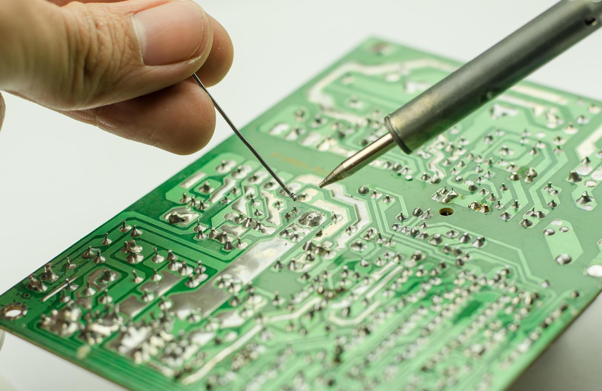
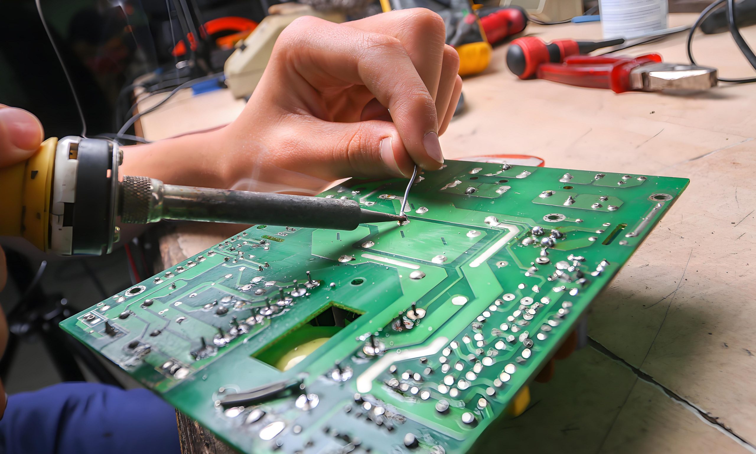
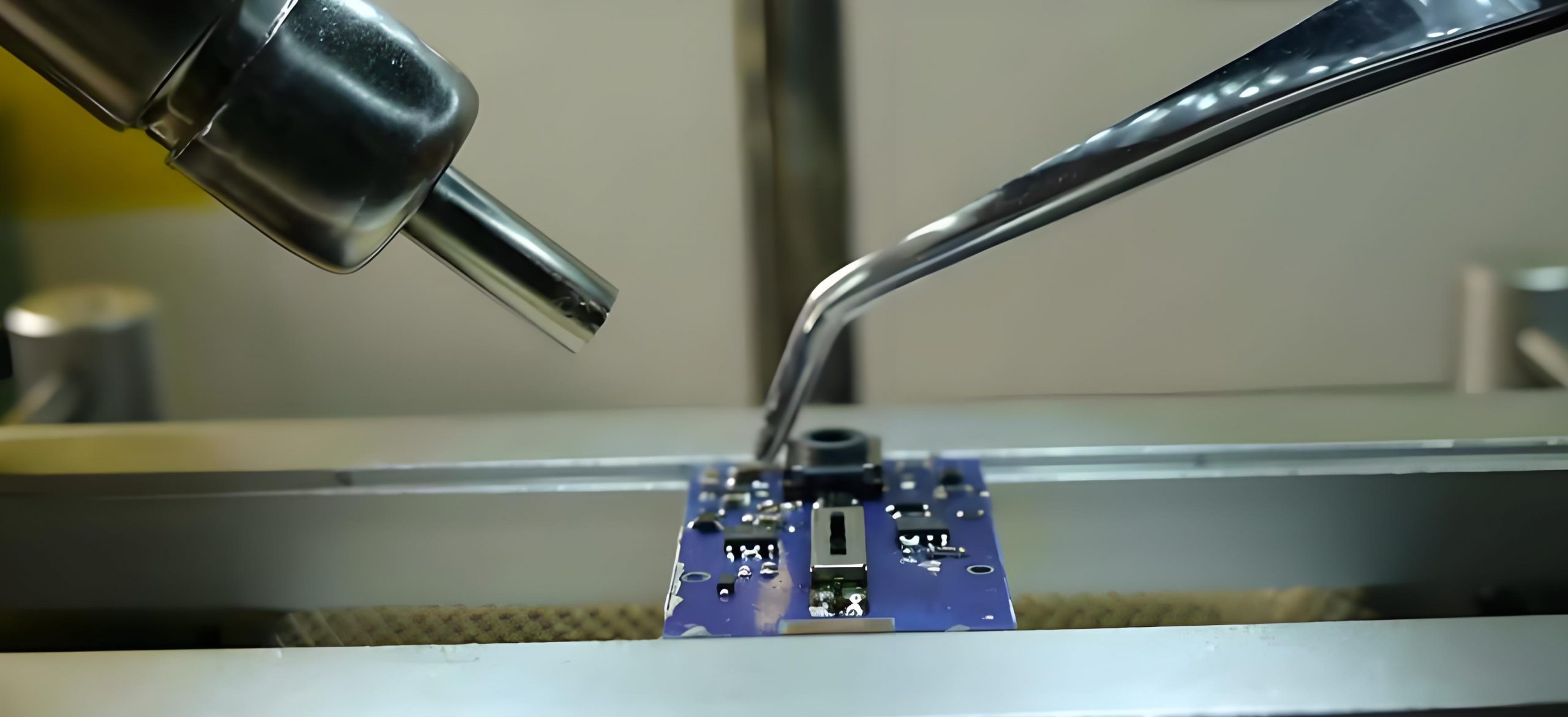
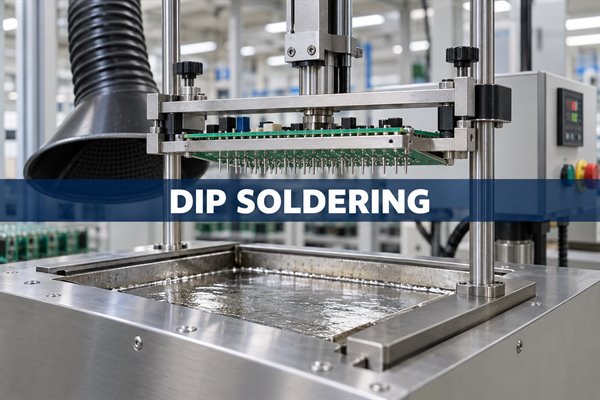
Dip soldering is a method in which component leads or the solder side of a PCB are lowered into a bath of molten solder. It is commonly used for through-hole components, terminals, connectors, and other leaded parts that can be soldered at the same time.
Dip and wave soldering both use molten solder, but the contact method is different. Dip soldering lowers the work into a mostly static solder bath. Wave soldering moves a PCB across a pumped wave of solder. That difference affects equipment, production speed, tooling, thermal exposure, and the types of assemblies each process handles well.
What Is Dip Soldering?
Dip soldering joins several exposed leads or PCB pads in one immersion. A fixture holds the assembly while the solderable area enters the bath. Component bodies, insulation, and areas that must remain free of solder stay above the solder line or are protected by a mask or pallet.
The method is often associated with through-hole PCB assembly, but it can also tin wire ends, terminals, tabs, and component leads before final assembly. The defining feature is direct immersion in molten solder, not the shape of the component package.
The process works best when the intended joints sit on a common plane and can receive similar heat. If some leads need much more heat than others, or if bottom-side components cannot be protected, a selective soldering nozzle or hand-soldering process may be easier to control.
How Does Dip Soldering Work?
A typical dip soldering cycle prepares the surfaces, applies flux and heat, immerses the joints, and then lets them cool before inspection. The equipment may be manual, semi-automatic, or programmable, but the physical sequence is similar.
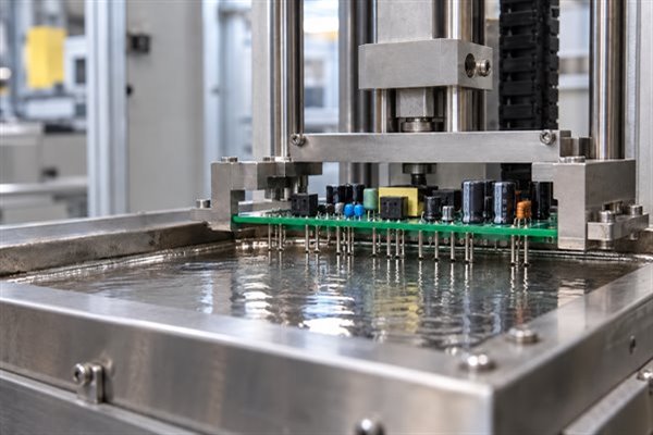
- Prepare the PCB and components: Check orientation, lead condition, pad cleanliness, and the area that will enter the solder. The board should sit securely in its fixture without allowing component bodies to touch the bath.
- Apply flux: Coat the exposed leads and pads evenly. Flux removes light oxides during heating and helps molten solder spread across the metal surfaces.
- Preheat the assembly: Warm the PCB so the flux can activate and the temperature change at immersion is less abrupt. Preheating also helps heavier joints reach soldering temperature during a short dip.
- Dip the solder side: Lower the fixture until the required leads and pads contact the molten solder. Depth and angle must remain steady so the solder line does not reach protected areas.
- Withdraw the board: Lift it smoothly at a controlled speed and angle. A stable exit lets excess solder drain away and helps prevent bridges and pointed solder projections.
- Cool and inspect: Keep the assembly still while the joints solidify. Then check wetting, bridges, hole fill, solder projections, residue, and any sign of heat damage.
The most sensitive part of the cycle is the short interval from preheat through withdrawal. Uneven flux, unstable immersion depth, or a slow exit can change the joint even when the solder-pot temperature has not moved.
What Temperature Is Used for Dip Soldering?
Sn63/Pb37 dip soldering commonly starts around 250–255°C, while SAC305 lead-free processes often use about 260–271°C. These are practical starting ranges, not universal settings. The correct value depends on the alloy, PCB thickness, copper area, component thermal mass, flux, immersion time, and required hole fill.
| Solder Alloy | Melting Range | Typical Pot Range |
|---|---|---|
| Sn63/Pb37 | 183°C | 250–255°C |
| SAC305 | 217–220°C | 260–271°C |
The melting data and common solder-pot ranges are consistent with published bar-solder alloy data and solder-pot operating guidance. A thick board with large ground planes may need more heat than a thin, lightly populated board even when both use the same alloy.
A bath that is too cool can produce slow wetting, incomplete hole fill, icicles, or long immersion times. Excessive temperature increases oxidation and dross, speeds copper dissolution, and raises the risk of damaged laminate, pads, masks, or components. The aim is to use enough heat for complete wetting without extending temperature or immersion time beyond what the assembly needs.
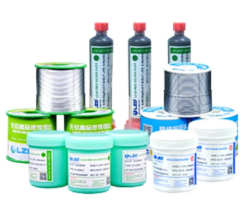
What Flux and Solder Are Used in Dip Soldering?
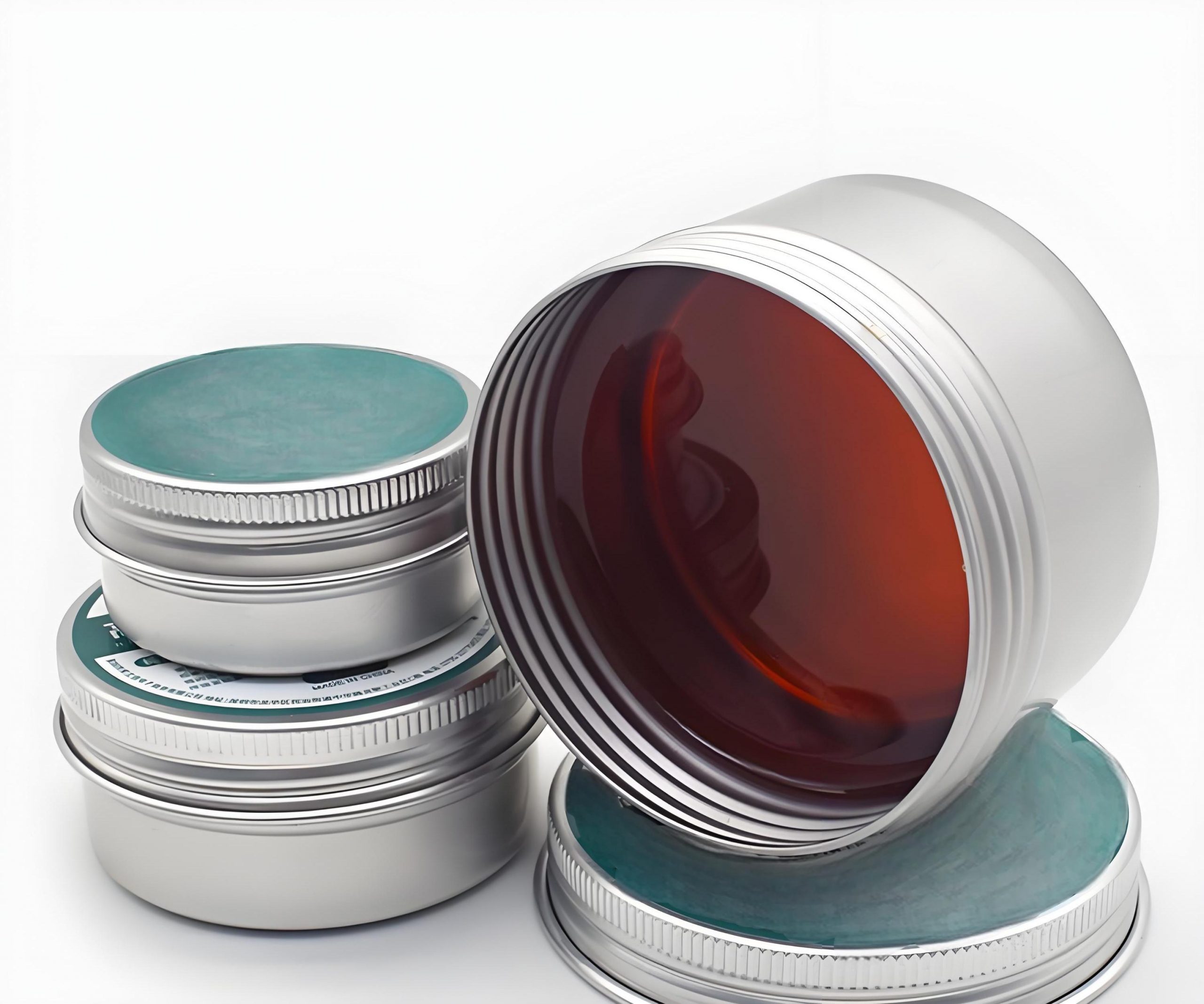
The flux must match the solder alloy, surface condition, cleaning method, and reliability requirements of the assembly. Its job is to remove light oxides and protect the metal long enough for solder to wet the lead and pad. More flux is not automatically better; excessive or poorly heated flux can spread residue and contribute to spatter.
- No-clean flux: Useful when the remaining residue is acceptable for the product and process. Apply only the amount needed and confirm that the preheat is suitable for the specific chemistry.
- Water-soluble flux: Offers strong oxide removal but normally requires thorough cleaning. The cleaning process must reach under components and around terminals before residues dry or become difficult to remove.
- Rosin-based flux: Used in some established soldering processes where its activity and residue behavior fit the product. Cleaning requirements depend on the exact formulation and assembly specification.
Sn63/Pb37 is a eutectic tin-lead alloy that melts at one temperature and wets readily, but its use is restricted in many products and markets. SAC305 is a common lead-free alternative with a higher melting range and greater thermal demand. Other alloys may be chosen for temperature, mechanical, regulatory, or compatibility reasons.
Flux and alloy should be selected together. A chemistry that performs well with tin-lead solder may need different preheat or contact conditions with a lead-free alloy. Before production, test the combination on a representative assembly and inspect the hardest-to-heat joints as well as the areas most likely to bridge.
Which PCBs and Components Are Suitable for Dip Soldering?
Dip soldering is most suitable when the required joints can enter the bath together and everything else can remain safely above the solder line. Straightforward through-hole layouts, accessible leads, and repeatable fixture support make the process easier to use.
- Through-hole connectors: Rows of connector pins or terminal blocks can be soldered in one controlled dip when their lead lengths and thermal loads are similar.
- Leaded electromechanical parts: Relays, switches, coils, transformers, and other components with exposed terminals may suit batch immersion when their bodies remain protected from heat.
- Single-sided solder areas: Boards with most solder joints on one accessible side are easier to fixture and mask than densely populated mixed-technology assemblies.
- Wire and terminal tinning: Wire ends, tabs, and terminals can be dipped to create a controlled tinned length before another joining operation.
- High-mix, moderate-volume builds: Changeable fixtures can make dip soldering practical when product variety is high and a full wave line would spend too much time in setup.
The process is less attractive when bottom-side surface-mount parts sit inside the immersion area, component bodies have low temperature limits, fine-pitch leads trap excess solder, or the board has large differences in thermal mass. In those cases, selective soldering or hand soldering may apply heat more precisely.
What Is Wave Soldering?
Wave soldering pumps molten solder through a nozzle to form a standing wave beneath a moving PCB. The assembly is fluxed and preheated before a conveyor or carrier passes its underside across the wave. Exposed through-hole leads and pads contact the flowing solder while protected areas stay behind a pallet or mask.
Because fluxing, preheating, conveyor speed, wave height, and cooling can be integrated into one line, wave soldering is well suited to repeated board designs and sustained production. The equipment and setup are more involved than a simple solder pot, but the process can deliver higher throughput once the line is balanced.
What Is the Difference Between Dip Soldering and Wave Soldering?
Dip soldering brings the assembly to a static solder bath; wave soldering brings a pumped solder wave to the moving assembly. This changes how the board is fixtured, how production flows, and where each process offers the clearest advantage.
| Factor | Dip Soldering | Wave Soldering |
|---|---|---|
| Solder contact | The PCB or leads enter a mostly static bath | The PCB passes across pumped molten solder |
| Production flow | Manual, semi-automatic, or programmed batch cycle | Conveyor-based inline or batch line |
| Typical volume | Prototypes, high-mix work, and moderate quantities | Stable designs and repeated higher-volume production |
| Tooling | Holder, depth stop, mask, or dip fixture | Carrier or pallet, conveyor setup, and wave nozzle |
| Key controls | Immersion depth, dip time, exit angle, and withdrawal speed | Conveyor speed, board angle, wave height, and pump setting |
| Changeover | Often easier for small or frequently changing batches | More setup is justified when the same board repeats |
| Throughput | Limited by fixture size and the dip cycle | Higher sustained output when the line stays loaded |
| Common risk | Uneven solder depth or bridging during withdrawal | Pallet shadowing, wave instability, or an incorrect conveyor profile |
Neither process is automatically better. The useful comparison is whether the actual board can be protected, heated evenly, and soldered at the required rate. A low-volume connector assembly may be simpler to dip, while a stable board with many through-hole joints may justify a wave line.
When Should You Use Dip Soldering Instead of Wave Soldering?
Choose dip soldering when the solderable area is clearly defined, product changeovers are frequent, and batch flexibility matters more than continuous throughput. Wave soldering becomes more attractive when the design is stable and production volume can keep an inline process busy.
- Choose dip for localized joint groups: A connector row, terminal bank, transformer, or small through-hole area can often be immersed without processing the full board through a wave line.
- Choose dip for frequent changeovers: A programmable lift and changeable fixture may switch between products faster than a conveyor line, although loading and alignment still need to be consistent.
- Choose dip for controlled batches: Prototype and moderate-volume work may not justify the floor space, solder inventory, and setup time of wave equipment.
- Choose wave for repeat throughput: A stable PCB family with many underside through-hole joints benefits from integrated fluxing, preheat, solder contact, and cooling.
- Choose selective soldering when immersion is unsafe: A mini-wave nozzle can target individual joints when bottom-side components, tight keepouts, or different thermal loads make full-area dipping impractical.
Before selecting the process, compare fixture needs, expected batch size, changeover frequency, component temperature limits, solder-side clearances, inspection effort, and likely rework. Those factors usually matter more than the name of the machine.
What Are the Most Common Dip Soldering Defects?
The most common dip soldering defects are bridges, incomplete hole fill, poor wetting, icicles, solder balls, disturbed joints, and heat damage. Their shape and location often point to the first process condition worth checking.
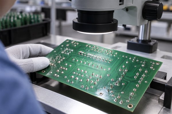
| Defect | Common Cause | First Check |
|---|---|---|
| Solder bridge | Excess solder, long leads, poor drainage, or unstable withdrawal | Lead length, exit angle, flux coverage, and withdrawal speed |
| Incomplete hole fill | Low joint temperature, weak flux action, poor solderability, or a heavy copper plane | Preheat at the cold joint, surface condition, and flux access to the hole |
| Nonwetting or dewetting | Oxidation, contamination, inactive flux, or an incompatible finish | Board and lead solderability before increasing bath temperature |
| Icicle or flag | Slow drainage, long leads, low joint heat, or poor exit motion | Withdrawal angle and speed, lead protrusion, and flux condition |
| Solder ball or splatter | Moisture, trapped solvent, rapid immersion, or a dirty fixture | Preheat, material storage, immersion rate, and fixture cleanliness |
| Disturbed joint | Movement while the solder is solidifying | Fixture stability and handling during cooling |
| Heat damage | Excessive bath temperature, immersion time, or solder depth | Thermal profile, solder line, pad condition, and component limits |
Do not correct every defect by raising the pot temperature. A bridge caused by withdrawal motion or a nonwetting lead caused by oxidation will remain until the actual cause is addressed.
How Can Dip Soldering Defects Be Reduced?
Defects fall when surface condition, flux, preheat, solder temperature, immersion, and withdrawal are kept consistent. The best adjustment starts with the defect pattern rather than a random change to several settings at once.
- Start with solderable surfaces: Keep boards and components clean, dry, and within their storage limits. If one material lot will not wet, check it separately before changing the whole process.
- Apply flux evenly: Make sure flux reaches every joint without flooding protected areas. Check both coverage and preheat when residue, spatter, or inconsistent wetting appears.
- Measure the actual assembly: A heater setting does not show what the coldest terminal or largest copper plane experiences. Profile representative hot and cold locations when hole fill varies across the board.
- Stabilize the solder bath: Keep temperature within the chosen range, remove dross without excessive agitation, and monitor alloy contamination. A dirty or oxidized pot can change wetting even when the display temperature looks correct.
- Control entry and exit motion: Repeatable depth prevents accidental component contact, while a smooth withdrawal gives excess solder time to drain. Review motion first when bridges or icicles follow a consistent direction.
- Inspect the result: Visual inspection should cover wetting, bridges, lead condition, solder projections, and visible hole fill. Electrical testing and additional inspection should follow the product risk and drawing requirements.
IPC J-STD-001 and IPC-A-610 provide widely used requirements for soldered assemblies and acceptance. The applicable revision, class, drawings, and customer requirements should define what an acceptable joint looks like for a specific product.
FAQs About Dip Soldering
Q1: Is dip soldering related to a DIP integrated-circuit package?
A1: No; the terms describe different things. Dip soldering is an immersion process, while DIP means dual in-line package. A DIP component can be hand soldered, wave soldered, selectively soldered, or dip soldered.
Q2: How long should a PCB stay in the solder bath?
A2: There is no universal dip time. Use the shortest stable contact that wets the joints and achieves the required hole fill without overheating the board or components. Board thickness, copper area, alloy, flux, and preheat all affect the result.
Q3: Can dip soldering be automated?
A3: Yes; programmable lift-dip machines can control depth, immersion time, and withdrawal speed. Automation reduces operator variation, but the fixture, thermal setup, solder condition, and inspection still need to suit the assembly.
Q4: Is nitrogen required for dip soldering?
A4: No, not for every process. Nitrogen can reduce oxidation and dross in some systems, but its value depends on the alloy, equipment, flux, solder exposure, production rate, and quality problems being addressed.
Q5: Is selective soldering the same as dip soldering?
A5: Not always. Dip soldering can be selective when a fixture exposes only certain joints, but selective soldering also includes mini-wave nozzles, multi-nozzle tools, robotic irons, and other targeted methods.
Q6: Can lead-free solder be used in a dip soldering pot?
A6: Yes, if the pot, flux, fixture, board, and components are compatible with the selected alloy. Lead-free alloys generally need higher temperatures than Sn63/Pb37, so thermal exposure and copper dissolution deserve closer attention.
Q7: How often should solder-pot contamination be checked?
A7: The interval should follow solder usage, operating time, alloy supplier guidance, and process history. Analyze the pot sooner when wetting changes, dross rises unexpectedly, or copper and other dissolved metals may be affecting the joints.
Need to decide whether dip, wave, or selective soldering fits your assembly? Send EBest Circuit your Gerber or ODB++ files, BOM, assembly drawing, quantities, target delivery date, solder-alloy restrictions, and inspection or test requirements at sales@bestpcbs.com. We can review the through-hole build and prepare a project-specific PCB assembly quotation with the proposed soldering route and tooling scope.