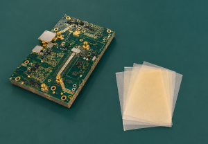
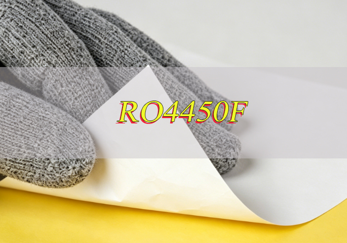
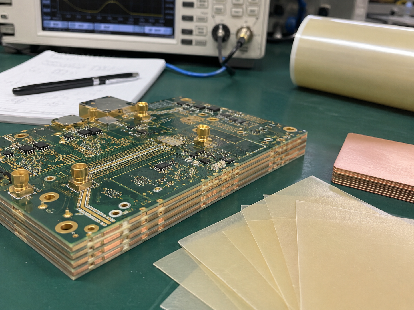
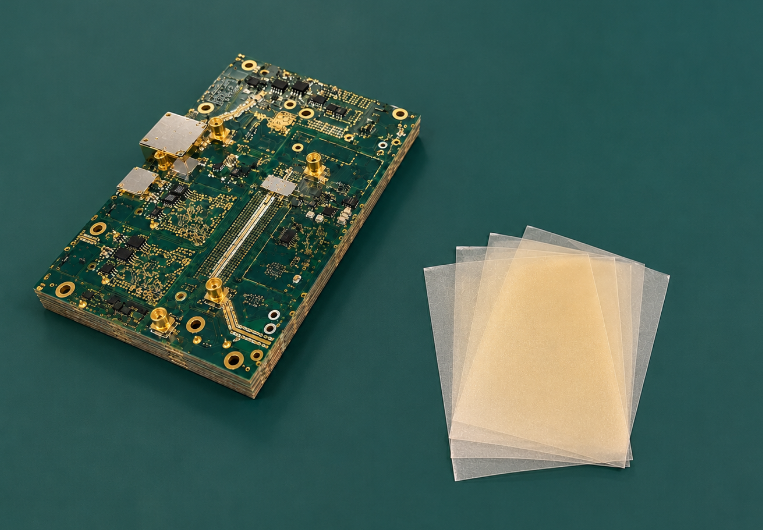
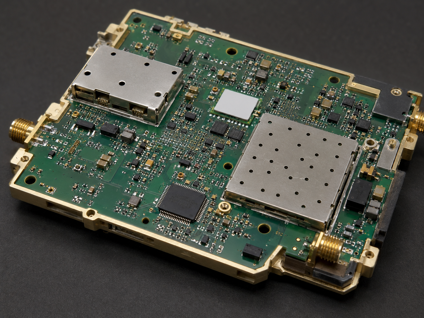
Rogers RO4450F prepreg is a high-frequency thermoset bonding material, also known as bondply, used to bond dielectric cores, copper layers, and copper foil in multilayer RF and microwave PCBs. It is generally considered when a design uses RO4000-series laminates and requires predictable dielectric spacing, reliable resin filling, controlled impedance, or sequential lamination. It is not a copper-clad core and is usually unnecessary for a simple two-layer board built from a single Rogers core.
EBest Circuit supports Rogers and Rogers/FR-4 hybrid PCB fabrication, including stackup review, controlled impedance, prototypes, and volume production. For an engineering review, send the Gerber files, proposed stackup, Rogers material grade, dielectric thickness, copper weight, target impedance, operating frequency, and quantity to sales@bestpcbs.com.
This guide covers RO4450F thickness, RO4450F Dk, compatible Rogers materials, lamination controls, and the information needed to quote a multilayer RF PCB.
What Is Rogers RO4450F Prepreg?
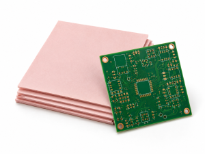
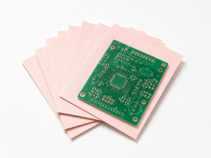
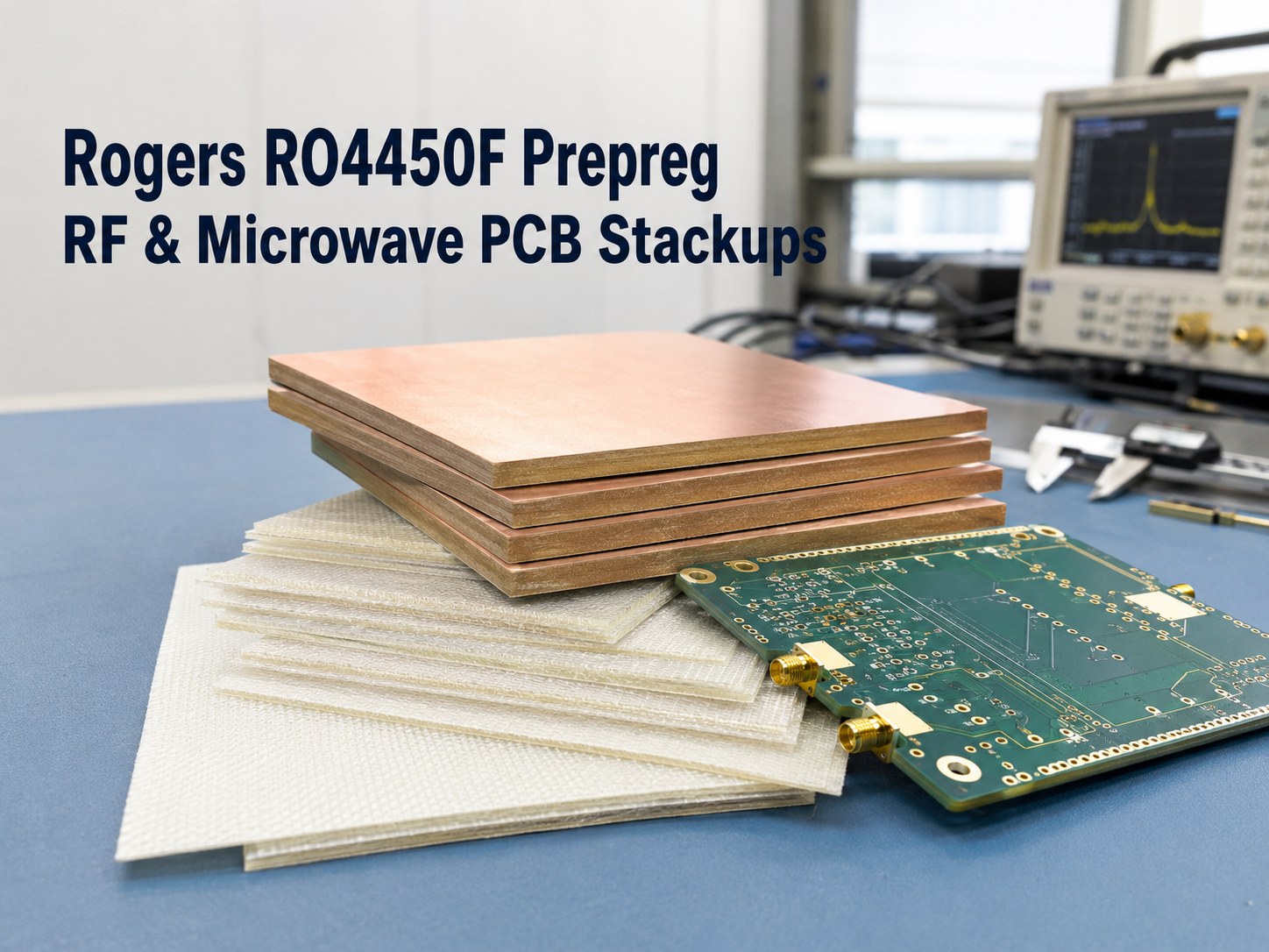
Rogers RO4450F is a glass-reinforced, hydrocarbon-ceramic thermoset bonding material in the RO4400 family. Before lamination, it is supplied as an uncured sheet without copper. During pressing, its resin softens, flows around etched copper features, and then cures to join the PCB layers.
After curing, RO4450F performs two functions:
- It provides mechanical bonding between the layers.
- It becomes part of the electrical dielectric structure.
This second function is especially important in stripline and other controlled-impedance structures. The bondply’s dielectric constant and final pressed thickness influence the distance between a signal trace and its reference plane.
RO4450F should not be described as a complete “RO4450F PCB laminate.” A laminate or core normally contains a cured dielectric with copper on one or both sides. RO4450F is the bonding layer placed between cores, inner layers, or copper foil.
It is appropriate for multilayer RF boards that need RO4000-compatible bonding. A two-layer RO4350B or RO4003C PCB made from one copper-clad core normally does not require bondply because no additional layers need to be laminated.
What Are the Key RO4450F Datasheet Values?
The following values come from the Rogers RO4450F and RO4460G2 bondply datasheet. They are typical material values rather than guaranteed finished-PCB results. Design teams should check the test method and obtain current material documentation before releasing a production stackup.
| Property | RO4450F typical value | Design relevance |
| Material type | High-frequency thermoset bondply | Used between layers, not as a copper-clad core |
| Standard thickness | 0.0040 in / 0.102 mm | Starting point for stackup planning |
| Thickness tolerance | ±0.0006 in | Must be considered in dielectric-height analysis |
| Dielectric constant | 3.52 ± 0.05 at 10 GHz | Influences impedance and signal velocity |
| Dissipation factor | 0.004 at 10 GHz | Contributes to transmission loss |
| Glass style | 1080 | Influences resin distribution and local dielectric behavior |
| Resin content | 80% | Supports filling around etched copper |
| Glass transition temperature | Above 280°C | Supports multiple lamination cycles after full cure |
| Decomposition temperature | 390°C | Indicates thermal decomposition resistance |
| Thermal conductivity | 0.65 W/m·K | Relevant to thermal modeling, but not a heat-spreading solution |
| CTE, X/Y/Z | 19/17/50 ppm/°C | Relevant to dimensional and plated-hole reliability |
| Moisture absorption | 0.04% under D24/23 conditions | Test conditions must be retained when comparing data |
| Flammability | UL 94 V-0 | Suitable for applications requiring this material rating |
| Lead-free compatibility | Yes | Compatible with lead-free assembly processes |
The Dk value of 3.52 should not be entered into every field solver without context. Rogers reports it using a defined IPC test method on raw material. Actual circuit behavior also depends on cured thickness, glass weave, copper roughness, trace geometry, frequency, and the measurement model used by the PCB manufacturer.
The official values and test conditions are available in the Rogers RO4450F bondply datasheet.
How Does RO4450F Work in a Multilayer PCB Stackup?
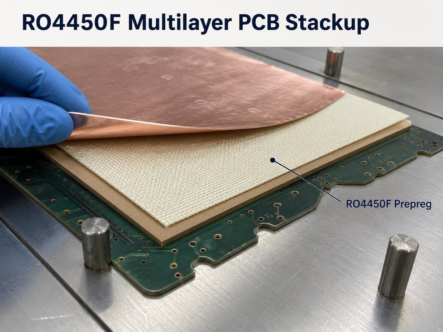
RO4450F is positioned between etched cores, inner-layer copper surfaces, or copper foil before the multilayer book is pressed. As the temperature rises, the resin reaches a low-viscosity range and flows into spaces around the copper pattern. Continued heat and pressure cure the resin and form a stable dielectric layer.
A typical multilayer construction may contain:
- An RO4350B or RO4003C RF core
- An etched inner copper layer
- One or more plies of RO4450F
- A reference plane or copper foil
- Additional Rogers or FR-4 layers
The bondply quantity cannot be determined from layer count alone. The manufacturer must examine copper thickness, retained copper percentage, open areas, opposing plane layers, venting features, and the required final dielectric spacing.
RO4450F is most valuable when its improved lateral flow helps fill a challenging copper pattern. However, adding more plies simply to improve filling also increases dielectric thickness. That can change impedance and may require different trace widths, so resin fill and electrical geometry must be reviewed together.
Which Rogers Laminates Are Compatible with RO4450F?
Rogers identifies RO4450F as compatible with multilayer constructions using RO4000-series materials, including RO4003C, RO4350B, RO4835, RO4360G2, and RO4000 LoPro laminates.
The most common pairings include:
- RO4003C: Often selected for commercial RF and microwave boards where performance and material cost must be balanced.
- RO4350B: Suitable for high-frequency multilayer designs that also require a UL 94 V-0-rated core material.
- RO4835 and RO4360G2: Used when their specific electrical, thermal, or environmental properties match the application.
- RO4000 LoPro: Useful when smoother copper is required to reduce conductor loss at higher frequencies.
Material compatibility does not mean that different cores can be exchanged without modifying the design. Each grade has its own Dk, Df, available thicknesses, copper options, thermal behavior, and processing requirements. Replacing RO4350B with RO4003C, for example, can change impedance and loss even if both can be bonded with RO4450F.
The exact core grade, copper foil type, dielectric thickness, and RO4450F ply count should therefore appear in the controlled stackup rather than being left to the manufacturer after quotation.
What Determines the Pressed Thickness of RO4450F?
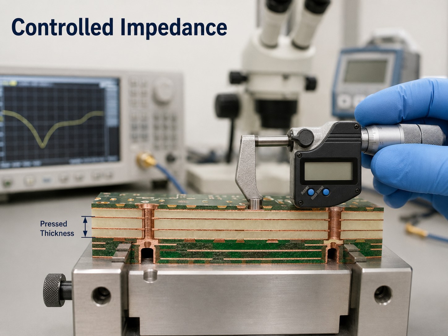
Each RO4450F ply bonds to approximately 0.004 inch, or 0.101 mm, when pressed between opposing flat surfaces. In an actual PCB, the thickness contributed by that ply changes because some resin moves into the spaces between copper features.
The main factors are:
- Inner-layer copper weight
- Percentage of copper remaining after etching
- Distribution of copper across the panel
- Plane-to-plane or signal-to-plane construction
- Number of RO4450F plies
- Lamination pressure and thermal profile
- Venting and flow patterns outside the functional circuit area
According to Rogers’ processing guidance, RO4450F can fill up to 0.0018 inch of total copper thickness under the stated design conditions. Additional bondply may be required when the filling requirement exceeds approximately 0.002 inch. This is particularly relevant to heavy inner copper and layers with large differences between dense and open copper areas.
A designer should not set controlled impedance from the nominal 4 mil value alone. The PCB manufacturer should calculate or estimate the finished dielectric thickness from the real copper pattern and validated press process. The resulting production stackup can then be returned to the designer for approval before fabrication.
How Does RO4450F Affect Controlled Impedance?
RO4450F affects controlled impedance whenever it forms part of the dielectric path between a signal trace and a reference plane. Both its Dk and its cured thickness influence the impedance result.
For an internal stripline, a thinner-than-expected RO4450F layer moves the trace closer to the reference plane and generally lowers impedance. A thicker layer generally raises impedance when the remaining geometry is unchanged. Trace width, copper thickness, trapezoidal etching, and copper roughness create additional variation.
The impedance review should include:
- Target single-ended or differential impedance
- Operating frequency or signal rise time
- Trace width and spacing
- Finished copper thickness
- Dielectric height above and below the trace
- Dk value and calculation method
- Copper foil type and roughness
- Manufacturing tolerance
- Coupon and test requirements
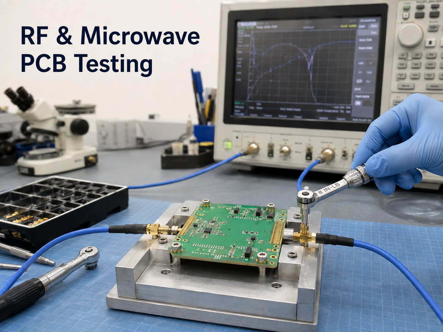
For RF transmission lines, insertion loss and phase behavior may be just as important as nominal impedance. A prototype should therefore be verified electrically when the stackup is new, the frequency is high, or the acceptable tolerance is narrow.
The drawing should identify the required impedance but allow the fabricator to make controlled trace adjustments after calculating the approved production stackup. Locking the trace geometry while leaving the final material construction undefined creates avoidable quotation delays and engineering questions.
Can RO4450F Be Used in Rogers and FR-4 Hybrid Stackups?
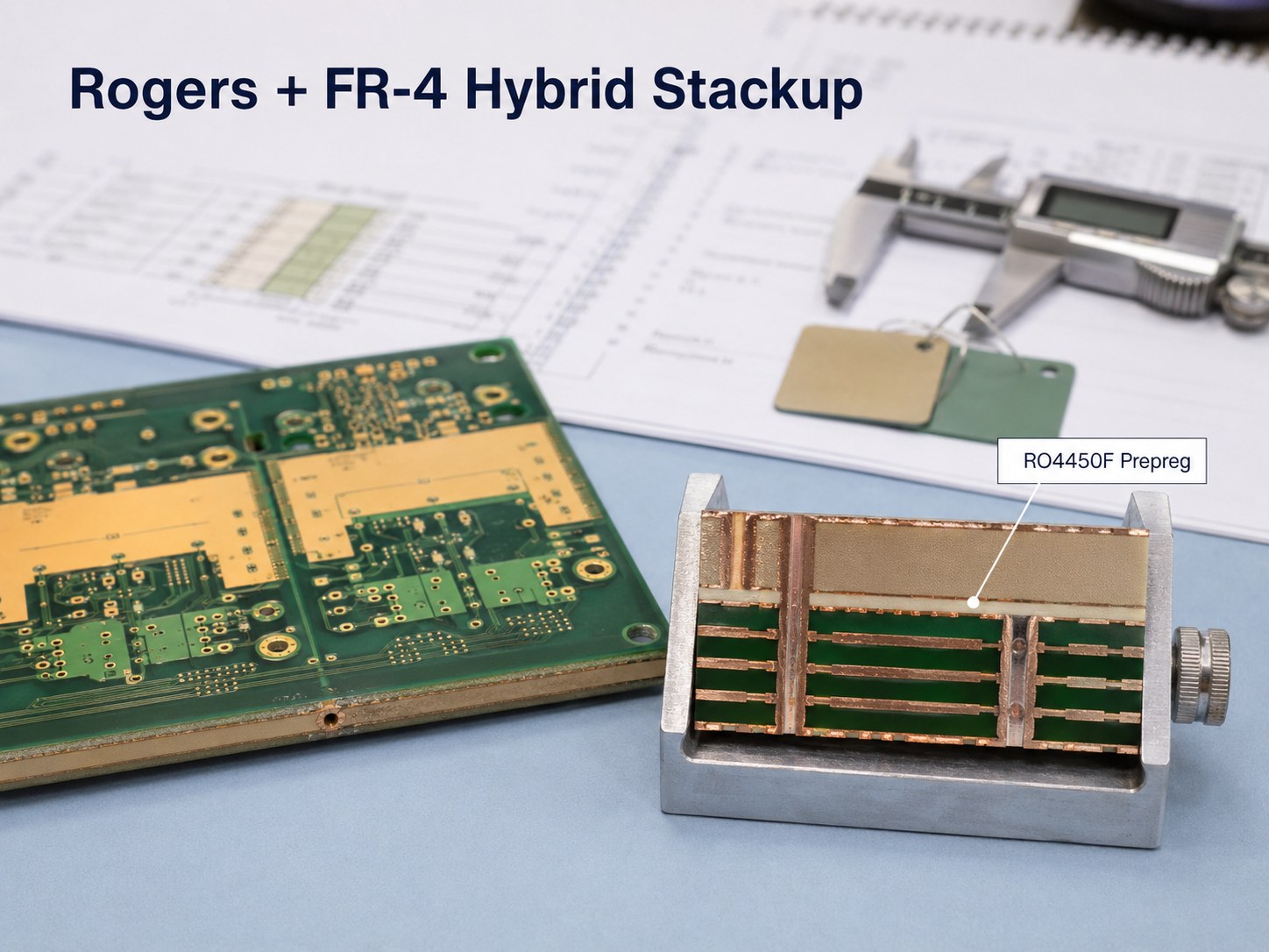
RO4450F can be used in selected Rogers/FR-4 hybrid multilayer constructions. Rogers states that RO4400 bondply uses FR-4-compatible bonding temperatures and can be combined with low-flow FR-4 bondply in a non-homogeneous stackup using one bonding cycle.
Hybrid construction can reduce material cost by placing Rogers laminates only where RF or high-speed performance requires them. Power, control, or low-speed routing layers may remain on FR-4 if their electrical and thermal requirements permit it.
However, the stackup must account for differences in:
- Dielectric constant and dissipation factor
- Z-axis and in-plane expansion
- Resin flow
- Copper adhesion treatment
- Glass transition behavior
- Moisture response
- Finished thickness and warpage
- Drilling and desmear requirements
Standard FR-4 prepreg should not automatically replace RO4450F next to an impedance-controlled RF trace. Its dielectric properties and loss may be unsuitable for that transmission-line structure. A hybrid approach works best when the electrical role of every dielectric layer is clearly defined.
Hybrid construction is unnecessary when every layer carries performance-sensitive RF signals or when the savings from replacing a small amount of Rogers material do not justify the additional stackup and process complexity.
How Does RO4450F Compare with RO4450B and RO4450T?
The correct choice depends primarily on approved legacy construction, resin-filling requirements, and the dielectric thickness options needed by the stackup.
| Selection point | RO4450F | RO4450B | RO4450T |
| Current design role | RO4000-compatible bondply with improved lateral flow | Referenced in earlier RO4400 documentation and existing designs | Spread-glass bondply with more thickness choices |
| Nominal thickness options | Primarily 0.004 in | Depends on the applicable legacy specification | Approximately 0.0025 to 0.006 in, depending on grade |
| Dk | 3.52 ± 0.05 at 10 GHz | Must be confirmed from the approved specification | Varies with thickness; not one universal value |
| Main advantage | Better filling for demanding copper patterns | May already be qualified in a legacy product | Greater dielectric-thickness flexibility |
| Best-fit decision | New designs or difficult fill conditions | Existing validated stackups | High-layer-count designs needing more thickness choices |
| Substitution approach | Review Dk, thickness, fill, and impedance | Do not replace based only on the family name | Recalculate the stackup for the selected thickness |
RO4450F should not replace RO4450B solely because it has better lateral flow. A substitution can change dielectric thickness, Dk, resin volume, impedance, and an already qualified thermal history. For an established product, review the material declaration, approved vendor list, validation records, and change-control requirements first.
RO4450T is more appropriate when the design needs finer control over dielectric spacing. RO4450F remains attractive when a 4 mil bondply fits the electrical geometry and copper filling is the stronger concern.
What Should Fabricators Check During RO4450F Lamination?
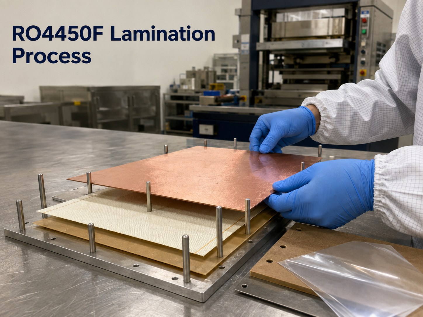
RO4450F lamination requires controlled storage, clean handling, suitable inner-layer preparation, and a press profile matched to the actual copper pattern.
Rogers’ processing guide identifies several important controls:
- Store the bondply at 10°C to 32°C and protect it from ultraviolet light.
- Keep unused material in sealed packaging and follow first-in, first-out control.
- Do not store it frozen, refrigerated, or under vacuum.
- Keep slip sheets in place during handling and tooling to limit contamination.
- Treat inner-layer copper with an appropriate oxide or oxide-alternative process.
- Bake prepared inner layers for 15–20 minutes at 115°C to 125°C before layup.
- Provide sufficient time in the 100°C to 120°C low-viscosity range for resin filling.
- Use vacuum assistance where available and verify the thermal profile with thermocouples.
- Maintain traceability for material lots, press cycles, and stackup records.
The published guide describes bonding pressures in the 400–750 psi range and a 175°C curing stage, but these numbers should not be copied into an uncontrolled press recipe. Board thickness, layer count, copper distribution, press equipment, book loading, and lagging materials influence the process window.
Special review is advisable for designs with more than six metal layers, copper of 35 µm or thicker, opposing plane layers, single bondply plies over demanding copper patterns, or bonding to FR-4 cores. The complete Rogers RO4400 processing guide should be used alongside the fabricator’s validated process.
What Causes Voids, Delamination, or Impedance Deviation in RO4450F Boards?
Most RO4450F defects originate from a mismatch between the copper structure, available resin, surface condition, and lamination process.
| Problem | Likely cause | Practical prevention |
| Resin voids | Insufficient resin, poor venting, contamination, or inadequate time in the flow window | Review copper topography, venting, ply count, cleanliness, and press profile |
| Delamination | Weak copper preparation, moisture, contamination, or incomplete cure | Control storage, inner-layer treatment, pre-bake, pressure, and curing records |
| Local thickness variation | Unbalanced copper or large open areas | Improve copper balance and calculate pressed thickness by layer |
| Impedance deviation | Incorrect Dk, dielectric height, trace width, or copper-thickness assumptions | Approve the production stackup and use impedance coupons |
| Registration error | Thin inner layers, unsuitable tooling, or excessive material movement | Match tooling and pinning strategy to the required registration tolerance |
| PTH reliability problems | Excessive thermal stress, unsuitable hole-wall preparation, or material mismatch | Inspect drilled holes and use a compatible desmear process |
| Surface discoloration or hardened sheets | Open-package exposure or poor inventory control | Reseal partial packs and discard visibly affected material |
Traditional chemical desmear should also be reviewed carefully. Rogers notes that CF4/O2 plasma is preferred when desmear is necessary, while etchback of the core and prepreg layers is not recommended.
Failure prevention is cheaper at stackup approval than after fabrication. A cross-section, impedance report, material certificate, electrical test, and controlled process record provide more useful evidence than relying only on the material name printed on the purchase order.
Which PCB Applications Use RO4450F?
RO4450F is best suited to multilayer boards in which Rogers RO4000-series cores require a compatible bonding layer and the cured bondply affects electrical or mechanical performance.
Common applications include:
- Backhaul radio equipment
- RF power amplifiers
- Small cells and distributed antenna systems
- Microwave communication modules
- RF filters and signal-distribution boards
- Antenna feed networks
- Test and measurement equipment
- High-speed communication hardware
- Mixed-material RF and digital multilayer PCBs
It is particularly useful when an RF design needs buried routing, internal reference planes, transitions between RF and digital sections, or multiple lamination cycles.
RO4450F may be unnecessary for a two-layer RF board, a low-frequency industrial controller, or a cost-sensitive design whose dielectric loss and impedance stability can be met with a suitable FR-4 system. Selecting it without a clear electrical or structural reason adds material cost and supply-chain constraints without creating a corresponding performance benefit.
What Information Is Needed for an RO4450F PCB Quote?
A reliable quotation requires more than the Gerber files and board dimensions. The manufacturer must understand the intended electrical geometry and which parts of the material specification are fixed.
Provide the following information:
- Gerber or ODB++ fabrication data
- Layer count and proposed stackup
- Exact Rogers core grades
- RO4450F ply location and quantity, if already defined
- Core and dielectric thicknesses
- Finished board thickness and tolerance
- Base and finished copper weights
- Controlled-impedance targets and tolerances
- Operating frequency or critical signal requirements
- Via types, finished hole sizes, and aspect ratios
- Surface finish
- Solder mask requirements
- Panel or individual board dimensions
- Prototype and production quantities
- Required inspection reports or impedance data
- Applicable acceptance class or customer specification
If the pressed dielectric height is not finalized, identify the electrical constraints rather than inserting an assumed value. The manufacturer can then propose a producible stackup for approval.
EBest Circuit can review Rogers and Rogers/FR-4 hybrid stackups before quotation. Sending the material grade, copper weight, target impedance, operating frequency, and proposed layer arrangement at the beginning reduces engineering questions and helps keep the prototype consistent with later production.
FAQs About Rogers RO4450F Prepreg
Is RO4450F a core or a prepreg?
RO4450F is a prepreg or bondply, not a copper-clad core. It is placed between PCB layers during lamination and becomes a cured dielectric after pressing.
Can RO4450F be laminated with RO4350B or RO4003C?
Yes. Rogers identifies RO4450F as compatible with RO4350B, RO4003C, and several other RO4000-series laminates. The complete stackup still needs review for thickness, impedance, copper filling, and lamination conditions.
What is the standard thickness of RO4450F?
The standard sheet thickness is 0.0040 inch, or approximately 0.102 mm, with a published tolerance of ±0.0006 inch. Its actual contribution to a PCB stackup depends on the copper thickness and distribution surrounding the bondply.
Can RO4450F be used with 1 oz or thicker inner copper?
It can be used with 1 oz copper, but the retained copper pattern and total filling requirement must be reviewed. Rogers recommends additional technical review for copper layers of 35 µm or thicker because a single ply may not provide enough resin for every pattern.
Can RO4450F replace RO4450B directly?
Not without engineering approval. Even materials from the same family can differ in thickness, Dk, availability, flow behavior, and qualification status, so the controlled stackup and impedance calculation must be checked.
Is RO4450F suitable for sequential lamination?
Yes. Its high post-cure Tg allows fully cured RO4400 bondply to withstand additional lamination cycles. The complete thermal history, via structure, and inner-layer preparation still need to match the fabricator’s validated process.
Can standard FR-4 prepreg replace RO4450F?
Standard FR-4 prepreg may be acceptable in non-critical layers, but it is not a direct electrical substitute near an RF transmission line. Differences in Dk, Df, thickness, and thermal behavior can change impedance, loss, and reliability.
RO4450F is a practical bonding material for multilayer RF PCBs when a design uses RO4000-series cores, requires controlled dielectric spacing, or presents demanding copper-fill conditions. Its nominal datasheet values are only the starting point; the final decision should be based on pressed thickness, copper distribution, impedance requirements, layer construction, and a controlled lamination process.
If you are planning a Rogers RO4450F multilayer PCB, send your Gerber files, stackup, material grades, copper weights, impedance targets, operating frequency, and quantity to EBest Circuit at sales@bestpcbs.com for engineering review and quotation.