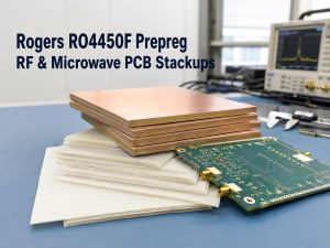
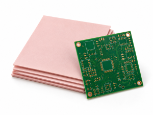
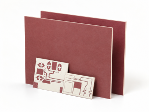
RO4450T prepreg is a Rogers ceramic-filled, glass-reinforced thermoset bonding material for multilayer RF PCBs. It bonds circuit layers together while forming part of the board’s dielectric structure. The correct selection includes the material grade, nominal thickness, copper layout and required finished dielectric spacing. A single Dk value does not describe every RO4450T construction. For example, Rogers lists a Dk of 3.23 for the 3 mil construction and 3.35 for the 4 mil construction at 10 GHz. This guide explains how those differences affect stackup selection, lamination and finished-board verification.
Key Takeaways
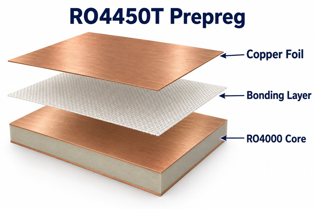
- RO4450T is a bonding layer for multilayer RF boards, not a copper-clad core.
- Dk and Df depend on the selected construction. Check the corresponding thickness row and test conditions before assigning material properties.
- Nominal prepreg thickness is not automatically the finished spacing between patterned copper layers.
- RO4450T and RO4450F are different materials. A substitution requires an electrical and manufacturing review.
- Lamination must control resin flow, filling and cure through the actual press book, not only the press setpoint.
- Material handling, cross-section inspection and impedance verification support repeatable RF stackups. Send the stackup and copper data with your RF PCB quotation request.
What Is RO4450T Prepreg Used For?
RO4450T bonds the layers of multilayer RF PCBs used in applications such as communications equipment, power amplifiers and small cells. During lamination, its resin flows around the circuit features and cures to join the stack.
The bonding layer matters electrically wherever the signal field passes through it. In stripline structures, for example, the dielectric around a trace can include both a core and a bonding layer. Giving the whole region the core’s Dk can produce the wrong impedance model.
At EBest Circuit, we support RF PCB fabrication with Rogers materials and stackup review. For a design specifying RO4450T, we review the requested construction, copper geometry and inspection requirements before confirming material sourcing and the manufacturing plan.
In material searches, “Rogers prepreg” and “Rogers bondply” can describe related bonding-material needs. The family name alone is insufficient for a fabrication drawing: identify RO4450T and its construction explicitly.
RO4450T Datasheet: Which Thickness and Dk Apply?
The RO4450T datasheet lists nominal thicknesses from 2.5 to 6 mil, with separate Dk and Df values for each construction. The table below follows the Rogers datasheet available when this article was prepared.
| Nominal thickness | Dk at 10 GHz | Df at 10 GHz |
|---|---|---|
| 2.5 mil / 0.064 mm | 3.26 ± 0.05 | 0.0037 |
| 3 mil / 0.076 mm | 3.23 ± 0.05 | 0.0039 |
| 3.5 mil / 0.089 mm | 3.19 ± 0.05 | 0.0033 |
| 4 mil / 0.102 mm | 3.35 ± 0.05 | 0.0042 |
| 4.5 mil / 0.114 mm | 3.29 ± 0.05 | 0.0044 |
| 5 mil / 0.127 mm | 3.28 ± 0.05 | 0.0038 |
| 6 mil / 0.152 mm | 3.24 ± 0.05 | 0.0044 |
Rogers reports these electrical values at 23°C and 50% RH using IPC-TM-650 2.5.5.5. They are material-characterization data, not a guarantee of a finished circuit’s impedance or insertion loss.
For simulation, document the construction, frequency and material model. A designer comparing a 3 mil and a 4 mil bonding layer must update both dielectric thickness and Dk; changing only the spacing leaves the model incomplete. Final line width also depends on copper thickness, etched trace shape and the adjacent reference planes.
How Does RO4450T Differ from RO4450F?
RO4450T and RO4450F differ in dielectric properties and material construction, so they should not be treated as drop-in replacements. Rogers’ published product comparison gives the following electrical values.
| Material | Published Dk | Published Df |
|---|---|---|
| RO4450T, 3 mil construction | 3.23 ± 0.05 | 0.0039 |
| RO4450F | 3.52 ± 0.05 | 0.0040 |
These are 10 GHz material values. The small Df difference alone does not establish which finished board will have lower loss: conductor roughness, geometry and route length also contribute.
When reviewing the RO4450F datasheet against RO4450T, compare the intended dielectric thickness, glass construction and processing guidance as well as Dk. Our RO4450F multilayer stackup guide covers the F-grade material separately.
If an approved design changes from F to T, revise the stackup and recalculate the affected transmission lines before releasing the board. Keep the material change visible in the fabrication revision rather than leaving a purchasing substitution undocumented.
Why Does Finished Dielectric Thickness Change?
Finished dielectric thickness changes because resin fills the spaces between copper features during pressing; copper thickness and pattern density affect how much resin remains above those features.
A nominal sheet value measured under a defined material test condition cannot describe every patterned circuit. Two regions with different copper coverage can impose different filling demands on the same bonding layer.
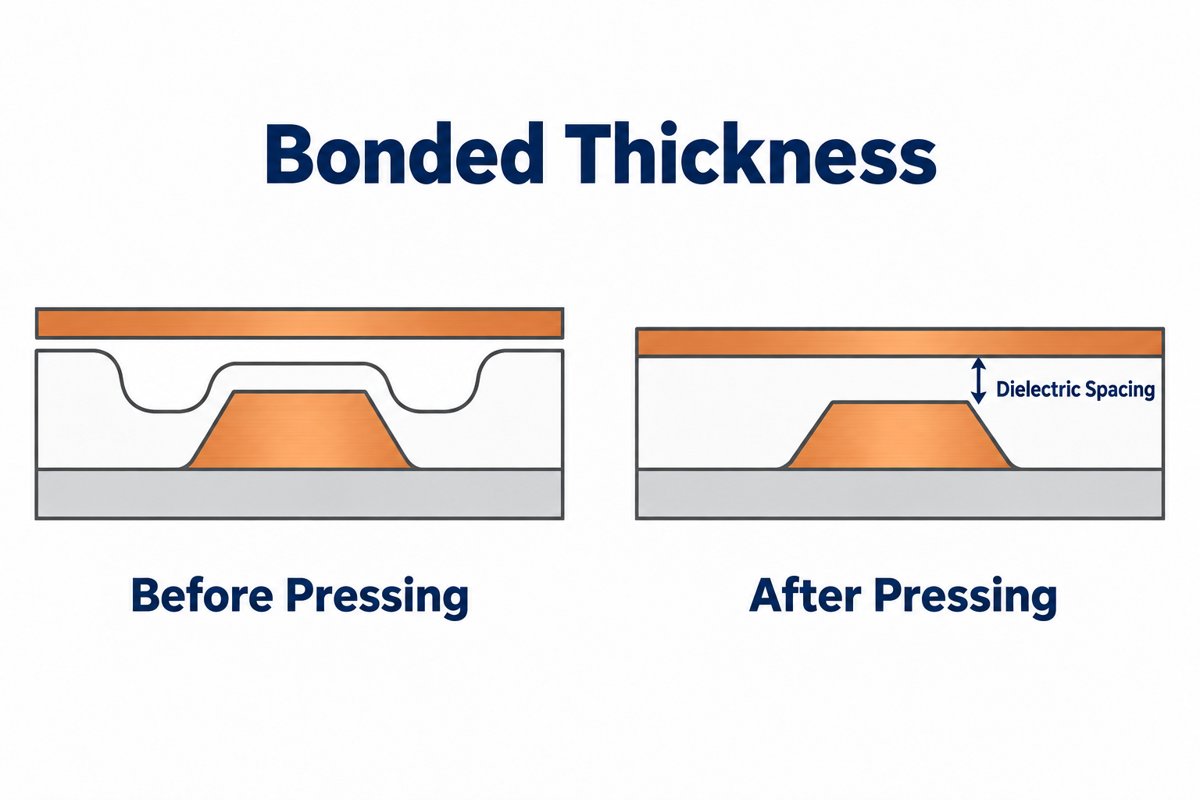
For an impedance-controlled layer, specify the required finished dielectric spacing and tolerance on the approved stackup. The fabricator then selects and qualifies a construction that can achieve it with the actual copper pattern.
- Provide copper artwork, not just the layer count and overall board thickness.
- Identify which signal layers reference which planes.
- Agree on the measurement location and acceptance range.
- Use a representative cross-section to verify the built spacing.
Adding nominal sheet values is useful for an initial thickness estimate, but it is not a substitute for a bonded stackup calculation.
How Should RO4450T Be Placed in the Stackup?
Place RO4450T at the bonding interfaces that need its dielectric performance, then define each adjacent core, copper layer and finished separation. Rogers identifies RO4835T as a matched core system; other combinations need their own stackup review.
Start with the electrical function of each layer rather than selecting every dielectric by the same material name:
- Locate RF traces and their continuous reference planes.
- Assign the core and bonding materials around those traces.
- Calculate line geometry using the selected constructions.
- Review copper balance and the mechanical symmetry of the full stack.
- Freeze the approved materials, dimensions and impedance targets in the fabrication package.
A hybrid board may combine RF materials with FR-4 in less electrically demanding regions. That can reduce the amount of RF material used, but it adds a material-compatibility and pressing review. Cost reduction should not remove the specified RF dielectric from a signal’s field region.
Keep the layer numbering and reference-plane assignments consistent between the CAD files and fabrication drawing. Our PCB design guidance provides a starting point for preparing the manufacturing information.
What Does RO4450T Lamination Require?
RO4450T lamination requires a controlled resin-flow stage followed by adequate cure, with the temperature measured through the press book. Rogers’ RO4400 processing guidance describes a low-viscosity window around 100–120°C and a 175°C cure dwell of 60 minutes.
Those reference conditions are not a complete recipe for every board. Press loading, copper distribution and the material combination determine how the book reaches the required conditions. Record the qualified cycle for the actual construction.
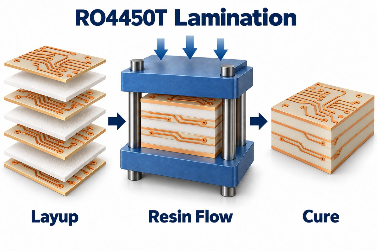
- Heat-up: verify the internal book temperature rather than relying only on platen temperature.
- Filling: confirm resin fills the patterned-copper topography without leaving voids or starving the interface.
- Pressure: qualify it together with the heat-up cycle and board construction.
- Cure: verify the specified dwell at the material, including the slowest-heating region.
For sequential builds, evaluate the cumulative thermal history and the interfaces already present. A successful first lamination does not by itself qualify later bonding cycles.
How Should RO4450T Prepreg Be Stored?
Store RO4450T in its sealed packaging under the supplier’s controlled conditions. Rogers’ RO4400 guidance specifies 10–32°C storage and a six-month shelf life from shipment when properly stored; it advises against refrigeration, freezing and vacuum storage.
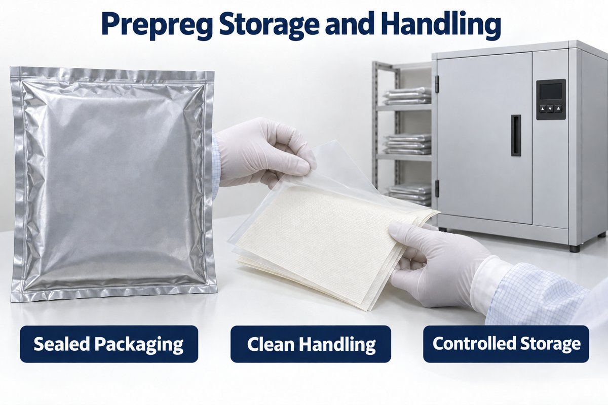
Use first-in, first-out lot control, reseal opened packages and follow any newer lot-specific instructions. Yellowing or hardened material requires disposition rather than routine release to production.
At receiving and material issue, record the grade, construction, lot and expiry information. Keep cut sheets clean and protected from creasing. If storage history is unknown, quarantine the lot for review; do not assume that a drying cycle restores its original processing behavior.
Which Manufacturing Defects Should Be Checked?
Check the bonded dielectric spacing, resin fill, interface integrity, drilled-hole condition and electrical performance. A board can pass continuity testing while still having a dimensional or RF-performance problem.
| Inspection | Primary check | Potential defect |
|---|---|---|
| Cross-section | Dielectric spacing and resin fill | Out-of-tolerance spacing, voids, resin starvation |
| Interface examination | Bonded-layer integrity | Separation or delamination |
| Hole-wall examination | Drilling, cleaning and plating condition | Residue, damaged walls, plating discontinuities |
| Impedance coupon | Specified transmission-line impedance | Geometry or dielectric deviation |
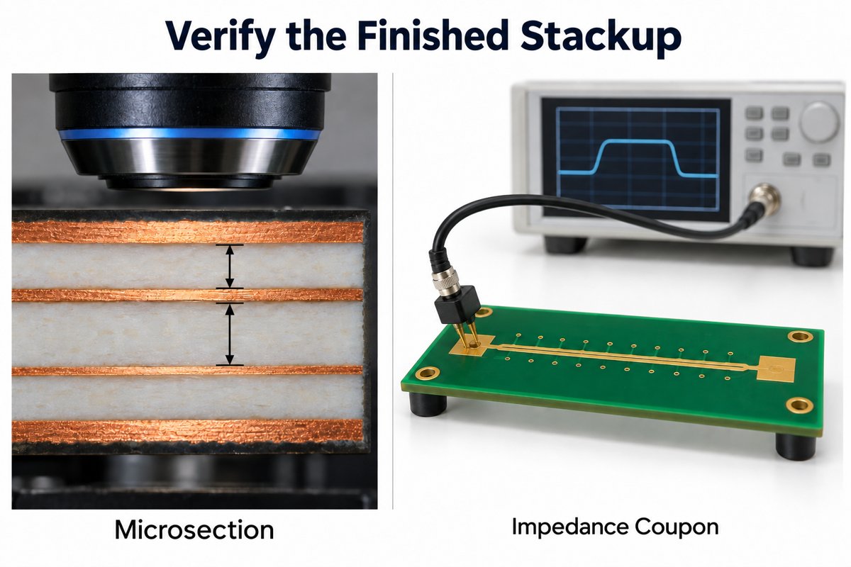
Rogers’ RO4835T/RO4450T processing guidance emphasizes assessing hole quality and choosing cleaning conditions accordingly. Aggressive etchback can disturb the material around the hole wall. Tool life and cleaning parameters therefore need process evidence, not assumptions copied from a different laminate.
Impedance testing and insertion-loss testing answer different questions. If the project has an RF loss limit, define the test frequency, structure and method separately. Do not treat a passing impedance coupon as proof that the entire RF path meets its loss budget.
What Should You Send for an RO4450T PCB Quote?
Send the fabrication files, proposed stackup, RO4450T construction and electrical requirements so we can evaluate the actual board rather than quote only a material name.
- Gerber or ODB++ data, drill files and fabrication drawing.
- Layer count, core materials and specified bonding-layer construction.
- Finished board thickness and critical dielectric tolerances.
- Starting and finished copper requirements.
- Impedance targets, tolerances and relevant RF test requirements.
- Surface finish, quantity and required delivery date.
- BOM, placement data and test instructions if assembly is included.
If the stackup is not final, identify which dimensions are fixed and which we may propose. Material availability, panel utilization, lamination complexity and inspection scope can all affect the quotation.
FAQ About RO4450T Prepreg
Is RO4450T a copper-clad laminate?
No. It is a bonding material. The copper foil and cured cores are separate elements in the multilayer construction.
Is a 3 mil RO4450T sheet equivalent to a 3 mil core?
No. A core is already cured, whereas the bonding sheet flows and cures during lamination. Their roles and finished-thickness behavior differ.
Can two RO4450T sheets be used to build a thicker bonding layer?
Multiple sheets may be considered in a qualified stackup, but the resulting bonded thickness and resin distribution must be evaluated. Two nominal sheet values do not automatically become the final dielectric spacing.
Does the material’s UL 94 V-0 rating certify the finished PCB?
No. A material flammability classification does not replace the finished PCB’s applicable recognition, construction limits or project qualification.
Can a generic “Rogers material” note replace the exact grade?
No. State the core and bondply grades separately and include the selected construction. Otherwise, the purchasing and manufacturing teams cannot reliably reproduce the intended dielectric stack.
How Can EBest Circuit Support Your RF PCB Project?
We support RF PCB manufacturing, DFM review and PCB assembly, helping you carry the approved material and stackup requirements into fabrication and assembly documentation.
For an RO4450T project, our review starts with the bonding-layer construction, copper pattern and finished dielectric target. We then confirm sourcing, manufacturing feasibility and the inspection scope with you. If a proposed material change affects the RF stackup, we raise it for approval before production.
Send your Gerber files and stackup to sales@bestpcbs.com. Include your impedance requirements and quantity, and we can review the build and prepare a project-specific quotation.