PCB manufacturing PCB manufacturing
Home > Blog

Electronic Product Design & Test

June 30th, 2026

Electronic product design & test is the complete process of turning an electronic idea into a stable, manufacturable, and testable product. It covers circuit design, PCB layout, component selection, prototype validation, functional testing, reliability checks, and preparation for mass production.

At Best Technology, our engineering work is closely connected with PCB fabrication, component sourcing, PCB assembly, prototype builds, and mass production. This gives customers a practical advantage: design decisions can be checked from the manufacturing side before they become expensive production problems. For projects that need OEM manufacturing, ODM development, sample validation, or custom engineering support, electronic product design and testing should begin before the first PCB is ordered.

What Is Electronic Product Design & Test?

Electronic product design & test means designing an electronic device and verifying that it works safely, reliably, and consistently before full production.

The design part usually includes product requirements, circuit architecture, schematic design, PCB layout, firmware coordination, enclosure fit, thermal planning, power design, and component selection. The test part checks whether those decisions perform correctly in real hardware.

In a PCB-based product, design and testing are strongly connected. A board may pass a basic power-on test but still fail under vibration, heat, EMI exposure, long operating time, or load changes. That is why professional electronic product testing does not stop at “does it turn on?” It checks function, stability, manufacturability, and production repeatability.

AreaWhat It CoversWhy It Matters
Circuit designSchematic, power rails, signal paths, protection circuitsDefines the product’s electrical behavior
PCB layoutStack-up, routing, grounding, impedance, spacingAffects EMI, heat, reliability, and assembly
Component selectionICs, passives, connectors, sensors, power devicesControls cost, availability, and lifecycle risk
Prototype testingBring-up, debugging, measurement, modificationFinds design issues before tooling or batch orders
Functional testingInput/output behavior, firmware response, load operationConfirms the product performs its intended function
Reliability testingThermal, aging, vibration, humidity, cyclingReduces field failure risk
Production testingICT, FCT, AOI, X-ray, final inspectionEnsures batch consistency

In short, electronic product design & test is the bridge between an idea and a product that can be manufactured repeatedly.

Why Is Electronic Product Design & Test Important?

Electronic product design & test is important because most product failures are cheaper to solve during design than after mass production.

A common mistake is treating testing as the final step. In reality, testing should influence the design from the beginning. Test points, programming access, fixture access, connector orientation, thermal margins, and inspection visibility all need to be planned early.

For example, if a PCB has no test pads for key voltage rails, factory functional testing becomes slower and less stable. If an RF trace is routed without proper impedance control, the prototype may work in a short bench test but fail in certification or long-range communication. If a high-current path is too narrow, the board may pass a short load test but overheat after extended use.

How Does Electronic Product Design & Test Work from Concept to Mass Production?

Electronic product design & test usually follows a staged process: requirement definition, design, prototype, validation, pilot run, and mass production.

The process starts with a clear product requirement. This includes input voltage, output power, operating temperature, expected lifetime, communication interface, mechanical size, certification market, and production volume. Without these details, engineers may design a board that works electrically but does not fit the enclosure, pass compliance, or meet cost targets.

For many hardware teams, EVT, DVT, and PVT are useful checkpoints. EVT checks whether the engineering concept works. DVT checks whether the design meets product requirements under more realistic conditions. PVT checks whether the product can be built consistently in a production environment.

How Does Electronic Product Design & Test Work from Concept to Mass Production?

What Are the Main Types of Electronic Product Design Services?

Electronic product design services can be divided into concept design, circuit design, PCB design, firmware coordination, mechanical integration, and production engineering.

Different customers need different service depth. Some customers already have a complete schematic and only need PCB layout optimization. Others have an idea, enclosure size, and performance target but need full ODM development.

Service TypeSuitable ForKey Deliverables
Concept-to-prototype designStartups, new product teamsArchitecture, schematic, PCB, sample
Schematic designCustomers with clear function requirementsCircuit diagram, BOM, design notes
PCB layout designHardware teams with existing schematicPCB layout, Gerber, stack-up
DFM/DFT reviewBuyers preparing productionManufacturing and testability feedback
Prototype developmentTeams before certification or toolingSample PCBA, debug support
Firmware coordinationEmbedded electronics projectsFirmware interface support
Component sourcingOEM/ODM production buyersAVL, BOM review, lifecycle check
PCBA manufacturingProduct brands and equipment companiesSMT, DIP, testing, final assembly

The best service model depends on how mature the project is. A mature design may only need design-for-manufacturing review and assembly testing. An early-stage idea needs deeper engineering support before PCB production begins.

Which Materials and Components Matter Most in Electronic Product Design?

For PCB-based products, material selection is not only about choosing FR4. The correct material depends on frequency, heat, voltage, mechanical structure, size, and environment. A low-power sensor may work well on standard FR4. A high-power LED product may need aluminum PCB or copper base PCB. A high-frequency communication product may need RF material with stable dielectric properties.

Design ItemCommon OptionsSelection Concern
PCB materialFR4, high Tg FR4, aluminum, copper base, ceramic, flexible PCBHeat, frequency, cost, reliability
Copper thickness1 oz, 2 oz, heavy copperCurrent capacity and thermal rise
Surface finishHASL, lead-free HASL, OSP, ENIG, immersion silverSolderability, flatness, storage life
ConnectorsWire-to-board, board-to-board, terminal blocksCurrent, vibration, mating cycle
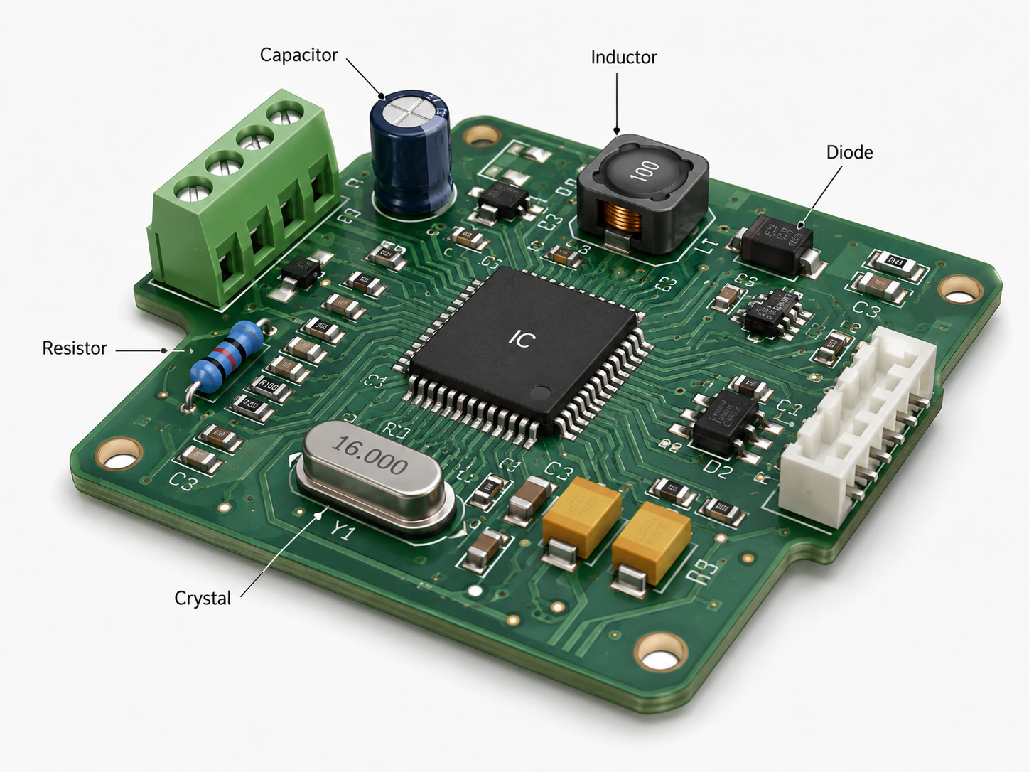
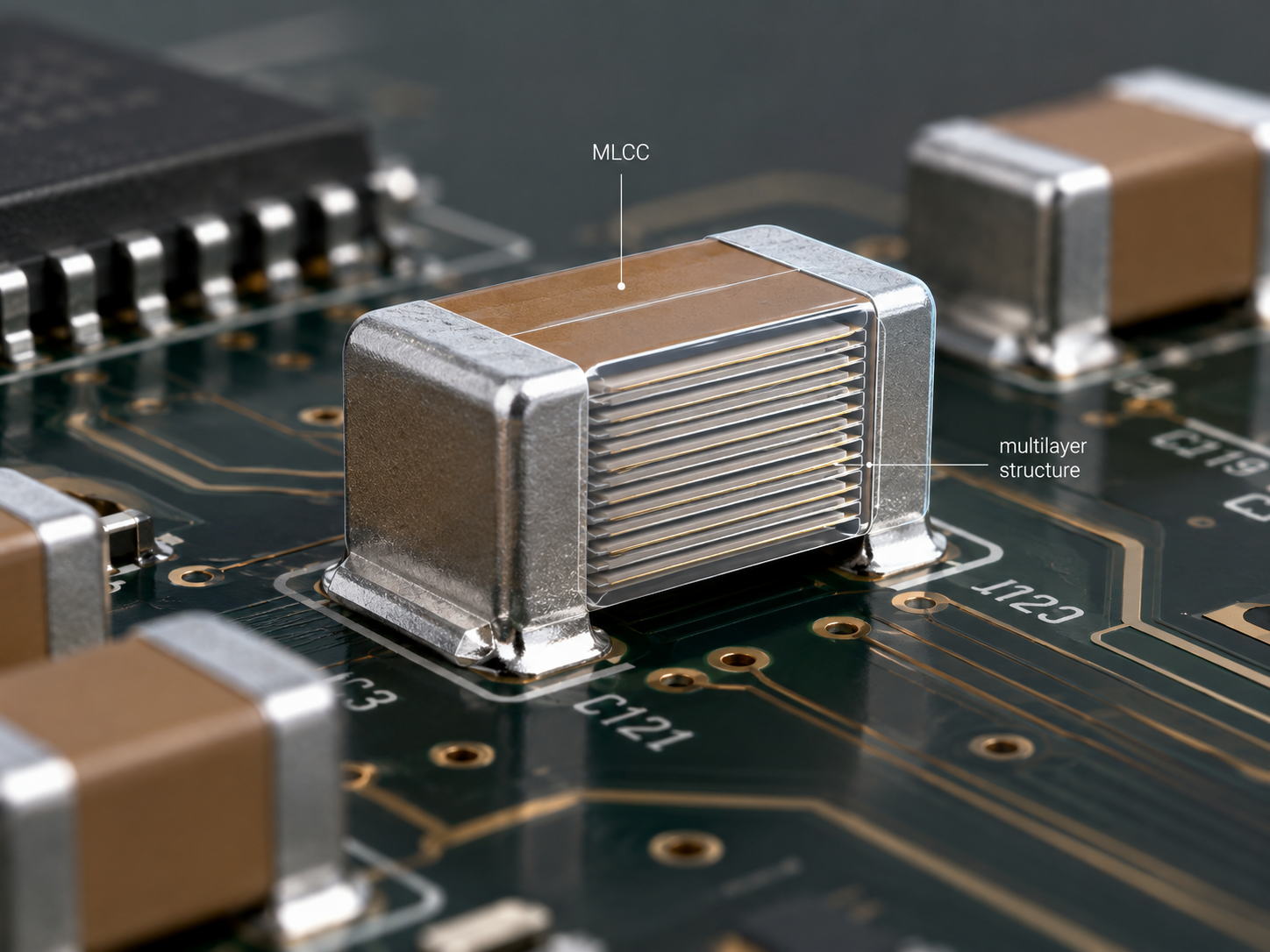
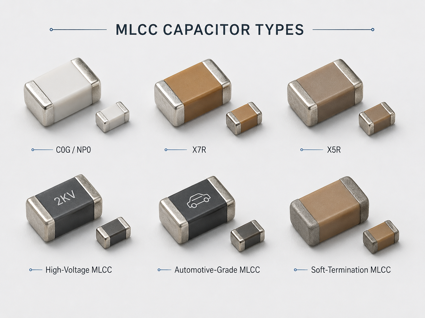
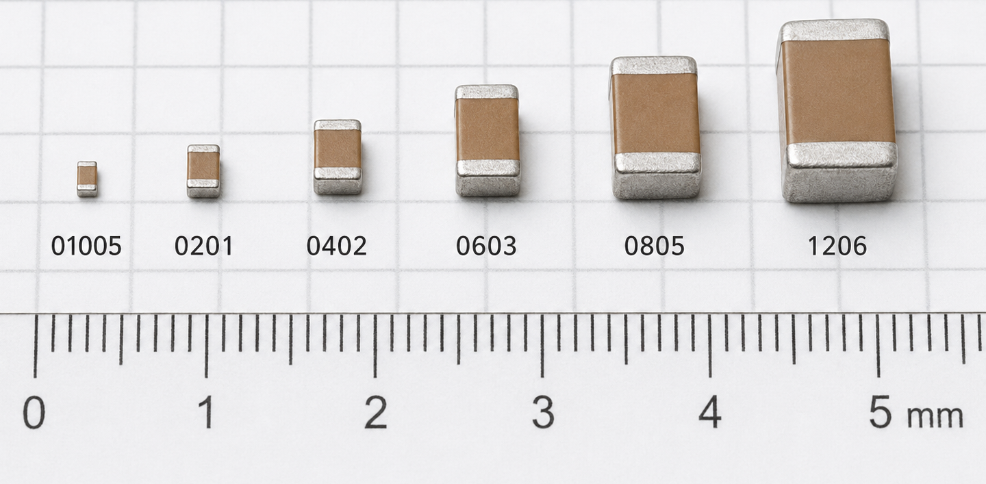
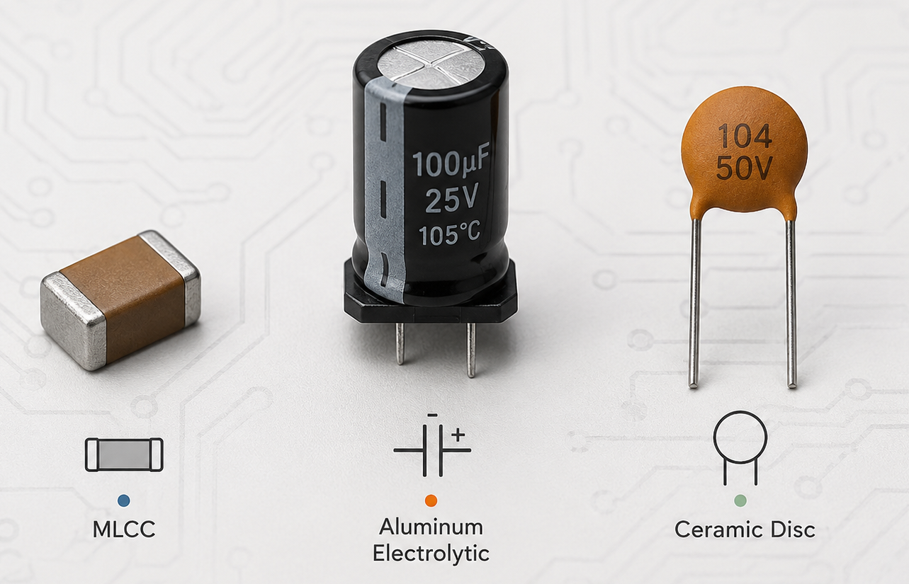
CapacitorsMLCC, electrolytic, tantalum, filmRipple current, polarity, voltage margin
Power devicesMOSFET, diode, regulator, driver ICHeat, efficiency, switching speed
SensorsTemperature, pressure, motion, opticalAccuracy, calibration, interface
Protection partsTVS diode, fuse, NTC, MOVSurge, ESD, overload protection

Component availability is also a design issue. A product may fail commercially if it depends on a part with long lead time, unstable supply, or a short lifecycle. For production projects, the BOM should be reviewed for alternatives, package availability, brand approval, and procurement risk before pilot production.

Which Materials and Components Matter Most in Electronic Product Design?

What Tests Are Used to Validate an Electronic Product?

Electronic product testing includes electrical tests, functional tests, reliability tests, safety checks, and production inspections.

The exact test plan depends on the product type. A medical device, automotive controller, LED driver, smart home module, and industrial sensor will not need the same test depth. However, most PCB-based products share several basic test layers, including:

Test TypeWhat It ChecksTypical Method
Visual inspectionAssembly defects, solder quality, missing partsManual inspection, AOI
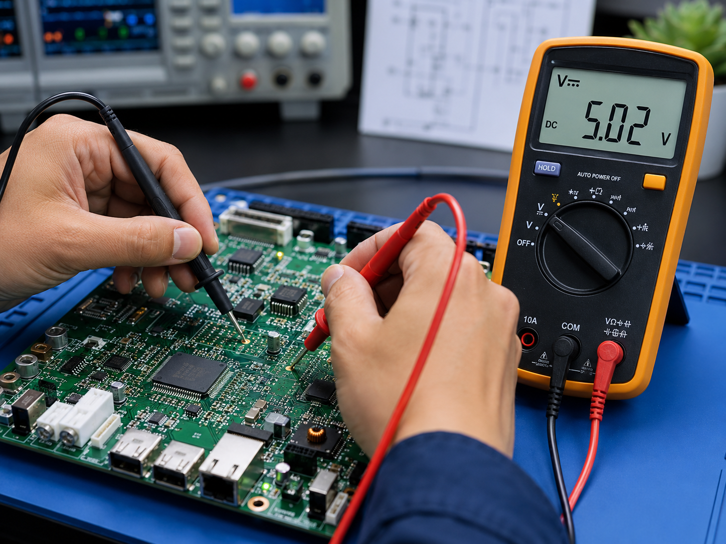
Electrical testShorts, opens, resistance, voltage railsMultimeter, flying probe, ICT
Functional testWhether the device performs its intended taskCustom test fixture, firmware test
Power testLoad behavior, efficiency, ripple, startupPower supply, oscilloscope, load meter
Thermal testHeat rise, hot spots, thermal stabilityThermal camera, chamber test
Signal testClock, waveform, impedance, communicationOscilloscope, logic analyzer, VNA
Aging testLong-time operation stabilityBurn-in rack, cycling test
Environmental testHeat, humidity, vibration, thermal shockEnvironmental chamber, vibration table
Safety testInsulation, creepage, clearance, protectionHi-pot, leakage, safety review
Production testBatch repeatabilityICT, FCT, AOI, X-ray, final QC

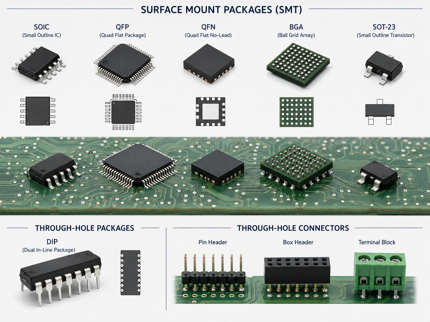
For assembled PCBs, AOI is useful for visible solder and placement defects. X-ray is important for hidden solder joints such as BGA, QFN thermal pads, and some through-hole conditions that cannot be fully inspected from the surface. Functional circuit testing checks whether the real product works under controlled factory conditions.

What Standards Should Be Considered During Electronic Product Design & Test?

For PCB and PCBA projects, IPC standards are commonly used for design, assembly workmanship, soldering process control, and acceptability. IPC-2221 is widely used as a foundation design standard for printed boards. IPC J-STD-001 focuses on soldered electrical and electronic assemblies. IPC-A-610 is commonly used for acceptability of electronic assemblies.

For products entering specific markets, safety and compliance requirements may also apply. IEC 62368-1 is widely relevant to audio/video, information, and communication technology equipment. Products with radio frequency functions may need FCC-related authorization for the U.S. market. Products entering the EU may need RoHS compliance for hazardous substance restrictions.

AreaCommon ReferencePractical Meaning
PCB designIPC-2221 seriesPrinted board design requirements
Soldered assembliesIPC J-STD-001Soldering materials, methods, and process criteria
Assembly acceptanceIPC-A-610Visual acceptability for electronic assemblies
Product safetyIEC 62368-1, IEC 61010, IEC 60601 depending on productSafety requirements by product category
Environmental complianceRoHS, REACH where applicableRestricted substances and material declarations
Wireless/RF productFCC, CE RED depending on target marketRF emission and equipment authorization
Automotive electronicsIATF 16949 system, customer-specific requirementsProcess control and traceability
Medical electronicsISO 13485 system, applicable medical device standardsQuality management and risk control

How to Choose the Right Design and Test Plan for Your Product?

The right design and test plan should match product risk, operating environment, market requirements, and production volume.

A simple consumer LED module may need schematic review, PCB layout, prototype testing, thermal check, and functional testing. A medical or automotive-related control board may need deeper documentation, traceability, reliability testing, risk analysis, and stricter inspection.

Use these questions before choosing the test plan:

  • What is the product’s input voltage and maximum current?
  • Will it operate continuously or intermittently?
  • What is the operating temperature range?
  • Does it contain RF, high-speed signals, motors, relays, batteries, or high-voltage sections?
  • Will it be used in consumer, industrial, automotive, medical, or outdoor environments?
  • What certifications or customer standards are required?
  • What is the expected production quantity?
  • What failure would be most costly: safety issue, downtime, warranty return, or certification delay?
How to Choose the Right Design and Test Plan for Your Product?

Which Industries Need Electronic Product Design & Test?

Electronic product design & test is needed wherever hardware must perform reliably after shipment.

The demand is especially strong in industries where PCB failure can cause downtime, safety concerns, service cost, or brand damage. These industries need more than basic PCB assembly. They need design review, process control, and test coverage matched to real operating conditions.

IndustryTypical ProductsMain Design and Test Concerns
Industrial controlPLC modules, sensors, motor controllersNoise immunity, connectors, long service life
Medical electronicsMonitoring devices, diagnostic modulesReliability, traceability, safety-related design
Automotive electronicsLighting, control modules, charging systemsVibration, temperature, process control
LED lightingDrivers, aluminum PCBs, power modulesHeat dissipation, current stability
Smart homeWi-Fi modules, sensors, control boardsRF performance, power consumption, safety
Consumer electronicsChargers, handheld devices, audio productsCost, size, user safety, durability
Communication equipmentRF boards, network devices, antennasImpedance, EMI, signal integrity
Energy productsBattery systems, inverters, power boardsHigh current, protection, thermal design

What Should Engineers Check Before PCB Manufacturing and Assembly?

Before PCB manufacturing and assembly, engineers should check manufacturability, testability, component risk, and production documentation.

If you required PCB assembly, then a clean Gerber package alone is not enough. The manufacturer also needs BOM, pick-and-place file, assembly drawing, test requirements, surface finish, material specification, copper thickness, impedance needs, and any special process notes.

Checklist ItemWhat to ConfirmWhy It Matters
Gerber and drill filesCorrect revision, complete layers, drill dataPrevents wrong board fabrication
Stack-upThickness, material, copper weight, impedanceControls electrical and mechanical performance
BOMPart number, brand, package, alternativesReduces sourcing and assembly risk
FootprintsPad size, polarity, pin orientationAvoids soldering and placement errors
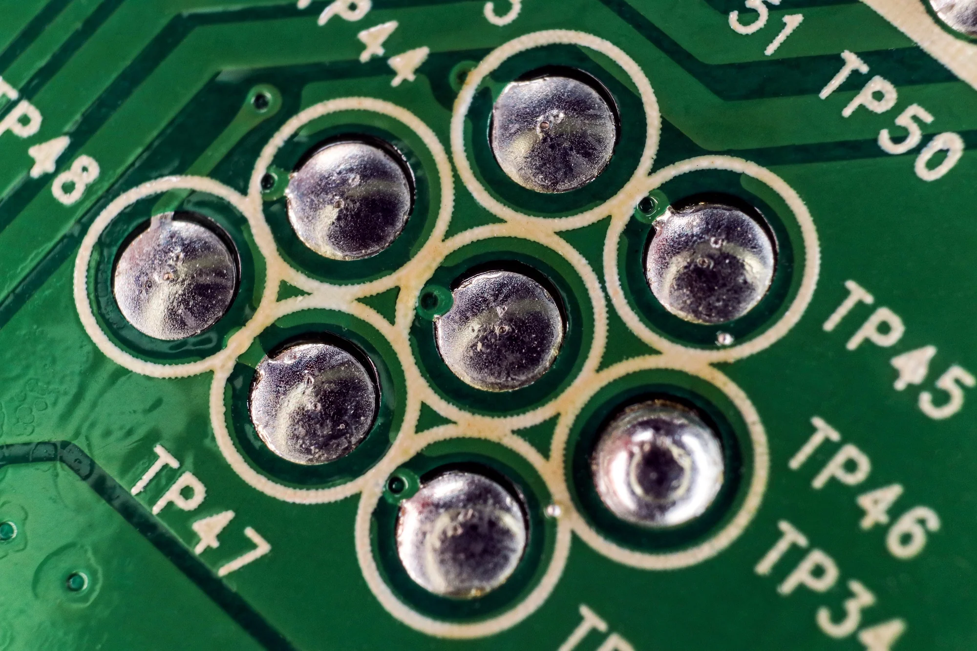
Test pointsPower rails, signals, programming padsImproves fixture testing
Thermal designCopper area, vias, metal core needControls hot spots
Creepage and clearanceHigh-voltage spacingSupports safety requirements
DFM reviewMinimum trace, spacing, annular ring, solder maskImproves manufacturability
DFT reviewFixture access, test sequence, pass/fail limitsImproves production consistency
Inspection planAOI, X-ray, ICT, FCTMatches product risk
PackagingESD protection, moisture control, labelingPrevents transport and storage damage

The best time to find these problems is before fabrication. Once PCBs are built and components are mounted, even a small design correction can require new boards, new stencils, and a new validation cycle.

What Affects the Cost of Electronic Product Design & Test?

The cost of electronic product design & test depends on design complexity, validation depth, component risk, PCB structure, test fixture needs, and production volume.

A simple two-layer control board is very different from a high-speed, high-current, RF, or medical-related product. The more constraints a product has, the more engineering time and test coverage it usually needs.

Cost FactorWhy It Changes Cost
Circuit complexityMore power rails, ICs, interfaces, and protection circuits need more design time
PCB layer countMultilayer boards require more layout planning and manufacturing control
Signal speedHigh-speed and RF designs need impedance control and measurement
Thermal demandHigh-power products may need aluminum, copper base, ceramic, or extra copper
Component availabilityHard-to-source parts increase BOM review and procurement work
Firmware interactionEmbedded testing may require programming and debugging support
Test fixtureCustom fixtures improve speed but add upfront cost
Reliability test depthAging, thermal cycling, vibration, and humidity testing increase validation cost
Compliance targetSafety, EMC, RF, or medical requirements add review and lab testing
Production quantityHigher volume often justifies better fixtures and stricter process control

Cost control should start with design decisions. Choosing a stable component package, avoiding unnecessary layer count, planning test pads, and using a manufacturable PCB structure can reduce total project cost without weakening product quality.

How to Choose a Reliable Electronic Product Design & Test Supplier?

A reliable supplier should understand both engineering design and manufacturing reality.

Many design problems happen because the design team and factory team work separately. The design may look elegant, but the PCB may be difficult to fabricate, hard to assemble, or slow to test. A better supplier can review the project from the full product path: schematic, PCB layout, BOM, fabrication, PCBA, testing, and shipment.

When selecting a supplier, check these points:

  • Can they support PCB design, prototyping, component sourcing, PCB assembly, and mass production?
  • Do they review DFM and DFT before production?
  • Can they explain which tests are needed and which are unnecessary?
  • Do they support AOI, X-ray, functional testing, and engineering feedback?
  • Can they handle custom PCB materials such as FR4, aluminum, copper base, ceramic, flexible PCB, rigid-flex PCB, or high-frequency PCB?
  • Do they understand OEM and ODM project workflows?
  • Can they support small-batch samples and later volume production?
  • Do they provide clear communication on technical files, BOM issues, and production risks?

For global buyers sourcing from a China-based source factory, the advantage is often stronger cost control, flexible customization, and direct manufacturing communication. The important point is transparency. A supplier should not claim fake local factories or local warehouses. Instead, it should clearly explain how engineering support, production, inspection, shipping, and documentation are handled.

Best Technology supports customers who need PCB design, PCB prototype, component sourcing, PCB assembly, and mass production from one engineering and manufacturing workflow. This is especially useful when customers need fast samples, custom PCB structures, or production feedback before placing larger orders.

Common Failure Analysis in Electronic Product Design & Test

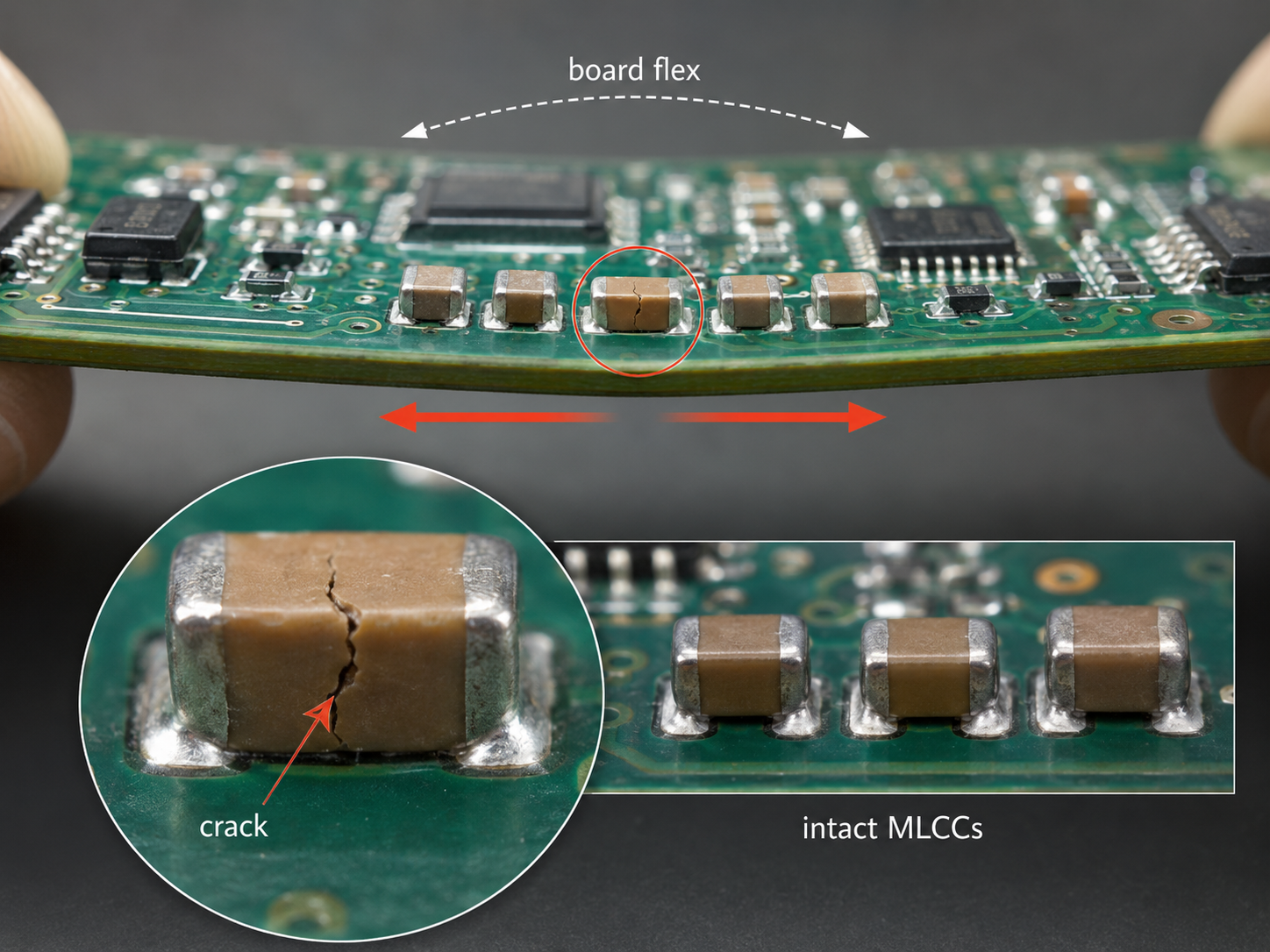
In real projects, failures are often caused by several small issues rather than one obvious mistake. A product may fail because of marginal component selection, weak thermal design, solder joint stress, firmware timing, poor grounding, or insufficient test coverage.

Failure SymptomPossible Root CausePractical Correction
Board does not power onShort circuit, wrong polarity, missing componentElectrical test, BOM check, polarity review
Random resetPower ripple, poor decoupling, firmware watchdog issueOscilloscope test, capacitor placement review
OverheatingNarrow copper path, weak heat spreading, poor airflowThermal simulation, copper increase, material change
Communication errorImpedance mismatch, EMI, grounding issueLayout review, shielding, signal measurement
High defect ratePoor footprint, solder mask issue, weak process windowDFM review, stencil tuning, AOI feedback
Field failureEnvironment not tested, vibration, humidity, agingReliability test and material review
Certification delayEMI or safety spacing issuePre-compliance review and layout correction

What Files Should You Prepare Before Requesting a Quote?

Before requesting a quote for electronic product design & test, prepare clear technical files and project requirements.

If the project is still at the idea stage, a block diagram, product function description, target size, expected power input, and use environment are helpful. If the project already has PCB files, send the Gerber, BOM, schematic, pick-and-place file, test requirements, and quantity.

File or InformationWhy It Helps
Product function descriptionHelps engineers understand the design target
SchematicAllows circuit review and debugging
Gerber filesNeeded for PCB fabrication review
BOMAllows component sourcing and assembly quotation
Pick-and-place fileNeeded for SMT programming
Assembly drawingShows polarity, placement notes, and mechanical details
Test requirementsDefines pass/fail criteria
Sample or reference productHelps compare function and structure
Target marketHelps identify compliance concerns
Quantity forecastHelps choose prototype, pilot, or mass production strategy

Clear files lead to faster quotation and fewer misunderstandings. They also allow the supplier to provide useful feedback before production starts.

FAQs

Q1: What is the difference between electronic product design and PCB design?

Electronic product design is the broader process. It includes product function, circuit architecture, schematic design, PCB layout, component selection, firmware coordination, testing, enclosure fit, and production planning. PCB design is one important part of that process. It focuses on board structure, routing, stack-up, grounding, spacing, and manufacturability.

Q2: Why should testing be considered during the design stage?

Testing should be planned during design because test access, fixture points, programming pads, and inspection visibility must be built into the PCB. If these items are added after layout, the board may need redesign. Early test planning makes production testing faster, more reliable, and easier to repeat during batch manufacturing.

Q3: What is the first step in electronic product development?

The first step is defining the product requirement. Engineers need to know the function, input voltage, output power, size, operating environment, target market, quantity, and compliance needs. Without these details, the design may work electrically but fail in cost, mechanical fit, certification, or production.

Q4: What tests are required for a new electronic product?

Most products need visual inspection, electrical testing, functional testing, power testing, and basic reliability checks. More complex products may need thermal testing, RF testing, EMI pre-checks, aging tests, vibration testing, humidity testing, or safety testing. The correct test plan depends on product risk and market requirements.

Q5: What is EVT in electronic product testing?

EVT means Engineering Validation Test. It checks whether the early engineering design works as intended. During EVT, engineers usually test power rails, main functions, interfaces, firmware behavior, signal quality, and thermal performance. EVT often produces a list of design changes before the product moves to deeper validation.

Q6: What is the difference between DVT and PVT?

DVT checks whether the completed design meets product requirements under realistic use conditions. PVT checks whether the product can be manufactured consistently through the planned production process. DVT focuses on design maturity. PVT focuses on production readiness, fixture stability, yield, process control, and batch consistency.

Q7: Can a manufacturer help improve my existing electronic product design?

Yes. A manufacturer with engineering capability can review schematic files, PCB layout, BOM, test points, material selection, assembly risk, and production files. This is especially useful when a product has unstable yield, overheating, sourcing problems, EMI concerns, or repeated assembly defects.

Q8: Why does a prototype work but mass production fails?

A prototype may be hand-built, manually tested, or assembled under special attention. Mass production depends on repeatable process windows. Problems often appear when footprints are marginal, test points are missing, components vary, soldering is difficult, or thermal margins are too narrow. Pilot production helps find these risks.

If you need support for electronic product design & test, PCB prototyping, PCB assembly, OEM manufacturing, ODM development, sample validation, or batch production, you can contact our engineering team at sales@bestpcbs.com for technical review and quotation support. 

You may also like

How to Wire, Mount and Test a PCB Relay Safely?

June 29th, 2026

A PCB relay helps a low-power control circuit switch a separate load circuit on a printed circuit board. It is widely used in industrial controls, home appliances, power modules, automotive electronics, security devices and automation boards. To use it safely, engineers must check coil voltage, contact rating, pinout, footprint, relay PCB layout, circuit protection, soldering quality and load conditions before prototype or mass production.

PCB Relay, https://www.bestpcbs.com/blog/2026/06/pcb-relay/

What Is a PCB Relay?

A PCB relay is a relay designed to be mounted directly on a printed circuit board. It allows a low-power signal to control a separate load circuit through isolated switching contacts. The relay usually has coil pins for the control side and contact pins for the load side.

Most board-mounted relays use through-hole pins because they provide stronger mechanical support and better current handling. Some compact signal relays may use surface-mount packages. In a relay control board, the component, footprint, copper width, solder joints and protection circuit all affect long-term reliability.

What Does a PCB Relay Do?

A PCB relay switches electrical loads on or off from a board-level control signal. Its main function is to separate the control circuit from the load circuit while allowing safe switching. This helps a microcontroller, sensor or logic IC control higher-voltage or higher-current devices.

The main functions include:

  • Switching AC or DC loads from a PCB.
  • Isolating low-voltage logic from higher-power circuits.
  • Controlling motors, lamps, heaters, fans, pumps and valves.
  • Supporting normally open, normally closed or changeover switching.
  • Reducing direct electrical stress on control components.

Therefore, this component is useful when isolation, simple control and reliable load switching are more important than high-speed switching.

How Does a PCB Relay Work?

A PCB relay works through a coil, armature and contact system. When the coil receives the correct voltage, it creates a magnetic field that moves the armature and changes the contact state. The contacts then open or close the load circuit.

When coil power is removed, a spring returns the armature to its original position. The load side and control side remain electrically separated. Because the coil is an inductive load, the circuit should include protection such as a flyback diode, TVS diode or snubber to reduce voltage spikes and protect the driver circuit.

Where Are PCB Relays Used?

PCB relays are used in products that require board-level control of external loads. They are common in industrial equipment, appliances, automotive electronics, power control boards and smart devices. The actual application depends on load type, current rating, voltage level, safety spacing and operating environment.

Common applications include:

  • Industrial automation controllers.
  • HVAC control boards.
  • Home appliance control modules.
  • Power supply and battery management boards.
  • Security alarm and access control systems.
  • Automotive auxiliary control circuits.
  • Test instruments and signal switching devices.
  • Smart home and IoT control products.

In these applications, the relay must match both the electrical load and the PCB manufacturing process.

What Are Types of PCB Relay?

PCB relay types can be classified by switching load capacity. This method is practical for PCB design because load capacity directly affects contact rating, copper width, pad size, heat rise, footprint area and relay cost. It also helps engineers decide whether the board needs a simple signal switch, a medium-load control part or a stronger power switching solution.

TypeLoad LevelTypical Use
Signal relayLow currentSignal routing, test instruments, communication boards
General-purpose relayLow to medium currentControl boards, small appliances, automation modules
Power relayMedium to high currentMotors, fans, lamps, heaters, pumps
High-current relayHigh currentPower boards, battery systems, industrial equipment

For real projects, the load type matters as much as the current value. A 5A resistive load is easier to switch than a 5A motor, solenoid or lamp load because inductive and inrush loads create stronger contact stress. Therefore, the relay should be selected according to actual load behavior, not only the rated current printed on the datasheet.

PCB relay types, https://www.bestpcbs.com/blog/2026/06/pcb-relay/

How Do You Choose the Right PCB Relay?

Choose a PCB relay by checking the load first, then the coil, footprint, protection design and supply risk. The right relay should match the real operating condition, fit the PCB layout and remain stable for future production. A part that works in a prototype may still fail in mass production if the footprint, derating, sourcing or test method is not reviewed.

  • Check coil voltage.
    Match the coil to the control supply, such as 5V, 12V or 24V. Wrong coil voltage can cause no action, buzzing, overheating or unstable switching. Also check pull-in voltage and release voltage, because a relay may not switch reliably if the power supply drops during operation.
  • Check contact rating.
    Confirm the rated voltage and current for the exact load type. AC and DC ratings are different, and DC loads usually need more margin because DC arcs are harder to break. For safety, the real load current should not be placed at the relay’s maximum limit.
  • Check load behavior.
    Motors, lamps, solenoids, valves and transformers can create inrush current or voltage spikes. These loads need higher contact margin and protection parts. If the load starts with a surge current, select the relay based on surge behavior, not only steady-state current.
  • Check contact form.
    Use NO when the load should turn on after energizing. Use NC when the load should stay on by default. Use SPDT or DPDT when one control signal must switch between two paths. Choosing the wrong contact form can make the device work opposite to the intended logic.
  • Check the PCB relay footprint.
    Confirm pin pitch, hole size, pad diameter, body outline and pin direction. Same pin count does not mean the same PCB footprint. Before fabrication, compare the datasheet view with the PCB library footprint to avoid reversed pinout or poor assembly fit.
  • Check coil drive current.
    If the coil current is higher than the MCU output rating, use a transistor, MOSFET, optocoupler or relay driver IC. The driver should have enough current margin, and the coil side should include suppression to protect the control circuit.
  • Check insulation spacing.
    High-voltage and high-current load copper should be separated from logic copper. Creepage and clearance must match the product safety requirement. For mains or high-voltage circuits, wider spacing, isolation slots or layout barriers may be required.
  • Check environment.
    Temperature, vibration, humidity and dust affect relay life. Industrial or automotive products may need better mechanical strength, heat resistance and vibration tolerance. If the product works outdoors or near motors, environmental stress should be reviewed early.
  • Check sourcing risk.
    Before mass production, confirm brand availability, approved alternates, lead time, certification and long-term supply stability. A relay with no second source may create production delays if the part becomes short or discontinued.

How Do You Read a PCB Relay Pinout?

A PCB relay pinout shows how the relay pins connect to the PCB pads. The coil pins belong to the control side, while COM, NO and NC pins belong to the switching side. The PCB relay symbol explains the circuit function, and the footprint defines the real pad, hole and pin spacing.

MarkMeaningFunction
CoilControl terminalsEnergizes relay
COMCommon contactMain switching point
NONormally openCloses when energized
NCNormally closedOpens when energized
SPSTSingle pole single throwOn/off control
SPDTSingle pole double throwChangeover control
DPDTDouble pole double throwTwo changeover paths

Always compare the datasheet top view or bottom view with the PCB footprint. A reversed pinout can make the circuit fail even when the schematic looks correct.

What Should Be Checked in a PCB Relay Circuit Design?

A PCB relay circuit design should be checked from both electrical and manufacturing angles. The most important items are coil drive capacity, contact rating, protection parts, trace width, creepage, clearance, soldering pads and load isolation. These points determine whether the relay can switch safely in real use.

AreaCheckRisk
Coil driveTransistor, MOSFET, driver ICMCU damage
ProtectionDiode, TVS, snubberVoltage spike
Contact pathCopper width, currentHeat rise
IsolationClearance, creepageShort circuit
Load typeMotor, lamp, heaterContact arcing
Pad designHole, annular ringWeak solder joint
Test accessCoil and contact netsHard debugging
Thermal designCopper balanceSoldering defect

For high-current or mains circuits, the layout must support the relay safety rating with proper copper spacing and insulation design.

How to Wire a PCB Relay Safely?

Wire a PCB relay by keeping the control side and load side separate. The coil connects to the driver circuit, while COM, NO and NC connect to the load path. The main goal is to prevent the load voltage or load current from entering the low-voltage control circuit.

1. Read the datasheet pinout.
Identify coil pins, COM, NO and NC before wiring. Check whether the drawing is top view or bottom view. This step prevents reversed footprint errors, which are common when the relay package looks symmetrical.

2. Connect the coil to a driver.
Do not drive most relay coils directly from an MCU pin. Use a transistor, MOSFET or relay driver IC when coil current is high. The MCU should only provide the control signal, while the driver carries the coil current.

3. Add coil protection.
For a DC coil, place a flyback diode, TVS diode or other suppression part near the coil. This protects the driver when the relay turns off. If fast release time is important, a TVS diode or diode plus Zener design may be better than a simple diode.

4. Wire the load through COM and NO or NC.
Use COM-NO for a load that turns on after energizing. Use COM-NC for a load that turns off after energizing. Label the contact function clearly in the schematic to reduce wiring mistakes during assembly and repair.

5. Separate high-power and low-power copper.
Keep load traces away from MCU, sensor, communication and low-voltage signal traces. This reduces noise coupling, short-circuit risk and safety spacing problems.

6. Size the copper path correctly.
The relay contact, PCB trace, solder joint and connector must all carry the load current safely. If any part of the path is undersized, the board may overheat even when the relay itself is correctly rated.

7. Add load-side protection when needed.
Motors, valves and solenoids may need snubbers, varistors, TVS devices or fuses. Protection should match the load type and voltage level. Without protection, relay contacts can arc, pit or weld.

8. Test before full power.
Check coil voltage, contact state, load polarity, fuse position and protection parts with a current-limited supply first. After the basic test passes, increase to the real load condition and monitor temperature rise.

What Common Precautions Should Be Followed When Using PCB Relays?

PCB relays common precautions should prevent coil damage, contact arcing, unsafe spacing and weak solder joints. A relay click does not prove the circuit is safe. The rating, layout, soldering quality and test result must all be checked. This is especially important for high-current, mains, motor and outdoor control products.

  • Do not exceed contact rating.
    Overload can cause contact welding, arcing, overheating and early failure. Always check the rating under the same load type, such as resistive, inductive, motor or lamp load.
  • Do not use the wrong coil voltage.
    Low voltage may cause buzzing or incomplete switching. High voltage may overheat the coil. Check actual coil voltage during operation, not only on the schematic.
  • Protect inductive loads.
    Motors, solenoids and transformers should use snubbers, varistors or TVS devices when required. This reduces contact arcing and extends electrical life.
  • Keep enough spacing.
    High-voltage load copper should not be close to low-voltage logic copper. Use wider spacing, isolation slots or separate copper areas when the product involves mains or high-voltage switching.
  • Avoid weak solder joints.
    Relay pins carry current and mechanical stress. Check hole size, pad size, hole fill and annular ring. Poor solder joints can cause intermittent switching, heat marks or field failure.
  • Control heat.
    Keep the relay away from hot power parts when possible. Check temperature rise under real load, especially when the board is enclosed or has poor airflow.
  • Follow soldering limits.
    Relay bodies, seals and pins may have soldering and cleaning limits. Do not wash the board unless the relay supports the cleaning process. Cleaning fluid inside an unsuitable relay can affect contact reliability.
  • Avoid routing sensitive signals under the load path.
    Relay load traces may carry surge current and switching noise. Keep them away from analog signals, RF lines, reset lines and communication buses.
  • Add test access.
    Provide test points for coil voltage, driver signal and load path if the board needs debugging or production testing. This makes failure analysis faster and reduces repair time.

How to Mount Relay on PCB?

Mount relay on PCB by checking footprint accuracy, insertion fit and solder joint quality. A relay should sit flat on the board without forced pin bending. Poor mounting can create weak solder joints, cracked holes, tilted parts and unstable contact during vibration.

1. Confirm the footprint.
Check pin pitch, hole size, pad size, relay outline, keep-out area and pin direction against the datasheet. Pay attention to top-view and bottom-view differences before PCB fabrication.

2. Check mechanical clearance.
Leave enough space around the relay body for insertion, soldering, inspection and heat dissipation. If a connector or enclosure is nearby, confirm the relay height and body outline.

3. Insert the relay gently.
The pins should enter the holes smoothly. Forced insertion can damage pins, plating or the relay body. If insertion is difficult, check the hole size and pin alignment instead of pressing harder.

4. Keep the relay flat.
A tilted relay creates uneven solder joints and weaker mechanical support. For larger relays, flat seating also helps reduce vibration stress on the pins.

5. Use the correct soldering method.
Through-hole relays are usually wave soldered or hand soldered. Control soldering temperature and dwell time. Excessive heat can damage the relay body or affect internal parts.

6. Avoid unsafe cleaning.
Flux-proof and sealed relays are not the same. Cleaning fluid can enter unsuitable relays and affect contact reliability. Confirm the relay sealing level before any washing or coating process.

7. Inspect after soldering.
Check hole fill, wetting, cracks, bridges, lifted pads and relay alignment. For high-current pins, solder quality is critical because poor joints can create heat and voltage drop.

8. Run a basic electrical check.
Confirm coil continuity, contact state and no short between control copper and load copper. This check should be completed before the board enters functional testing.

Mount Relay on PCB, https://www.bestpcbs.com/blog/2026/06/pcb-relay/

How to Test a PCB Relay?

Test a PCB relay by checking the coil, contact action, driver circuit and load path. Testing should confirm both relay movement and real electrical switching. A relay that clicks may still have burned contacts, wrong wiring or a failed load path.

1. Disconnect power.
Turn off the board and discharge capacitors before measuring. This protects the technician, meter and PCB from accidental short circuits.

2. Identify pins.
Use the datasheet to locate the coil, COM, NO and NC pins. Do not guess by package shape because similar relays may use different pinouts.

3. Measure coil resistance.
Use a multimeter to check the coil. An open reading may mean a broken coil. A very low reading may mean a shorted coil. Compare the result with the datasheet range when available.

4. Apply rated coil voltage.
Use a current-limited supply. The relay should switch clearly without buzzing or overheating. If it buzzes, check supply voltage, driver current and coil rating.

5. Check contact continuity.
Measure COM-NO and COM-NC before and after energizing the coil. The contact state should change correctly. If the state does not change, the contact system may be damaged or the wrong pins may be tested.

6. Check the driver circuit.
If the relay does not work on the board, test the transistor, MOSFET, diode, control signal and coil supply. Many relay failures are actually caused by a failed driver or missing control voltage.

7. Check the load path.
Measure voltage at the load input and output side. If the relay clicks but the load does not work, the issue may be a fuse, connector, trace, solder joint or burned contact.

8. Test with the real load safely.
Confirm stable switching, no abnormal heat, no contact sticking and no voltage drop on the load path. For motors or inductive loads, repeat switching cycles to check contact stress.

PCB Relay Test, https://www.bestpcbs.com/blog/2026/06/pcb-relay/

What Are Common PCB Relay Problems and Failure Signs?

Common PCB relay problems are usually caused by wrong selection, poor protection, weak soldering or overload. The relay should be checked together with the driver circuit, load path and PCB copper. Replacing only the relay without correcting the root cause can lead to repeated failures.

  • No click when powered.
    Possible causes: wrong coil voltage, open coil, failed driver, broken trace or missing control signal.
    Prevention: verify coil voltage, driver current and control signal during prototype testing and production inspection.
  • Clicking but no load output.
    Possible causes: wrong COM/NO/NC wiring, burned contacts, no load supply, blown fuse or cracked solder joint.
    Prevention: check contact continuity, load voltage and fuse status during functional testing.
  • Contact sticking.
    Possible causes: overload, high inrush current, inductive surge or undersized contact rating.
    Prevention: choose higher contact margin, add surge protection and avoid switching loads beyond the rated category.
  • Relay buzzing.
    Possible causes: low coil voltage, unstable supply, weak driver current or wrong coil type.
    Prevention: measure coil voltage during actual switching and keep enough power supply current margin.
  • Overheating.
    Possible causes: high current, narrow PCB traces, weak solder joints, poor connector design or nearby hot components.
    Prevention: review trace width, solder quality, connector rating, airflow and temperature rise under real load.
  • Intermittent switching.
    Possible causes: cracked solder joints, vibration, oxidized contacts or unstable coil drive.
    Prevention: improve pad design, inspect solder joints, secure heavy components and select a relay suitable for the environment.
  • Burned pads or traces.
    Possible causes: excessive current, arcing, poor copper width or loose load connection.
    Prevention: calculate current path, check connector rating, add protection and test under the real load before mass production.
  • Short relay life.
    Possible causes: frequent switching, inductive load, high inrush current, heat or wrong relay category.
    Prevention: confirm electrical life under real load conditions and choose a relay with enough switching-cycle margin.

How to Remove Relay from PCB Board?

Remove relay from PCB board only after the solder is fully cleared from every pin. Pulling the relay by force can lift pads, damage plated holes and break copper traces. Careful removal is important because relay pins are often larger and harder to desolder than small signal components.

1. Disconnect all power.
Remove external power, load wiring and stored energy from capacitors. If the board controls AC or high-current loads, confirm the circuit is fully isolated before handling.

2. Mark the relay direction.
Take a photo before removal so the replacement part is installed correctly. This helps prevent reversed installation, especially when the pin layout is not symmetrical.

3. Add flux or fresh solder.
This improves heat transfer and makes old solder easier to remove. Old solder can be difficult to clear if the board has large copper areas connected to the relay pins.

4. Desolder each pin.
Use a desoldering pump, braid or vacuum desoldering tool. Work slowly on every through-hole pin. Avoid heating one pad for too long because excessive heat can lift copper pads.

5. Check pin movement.
Gently move each pin. If one pin is still fixed, continue desoldering instead of pulling. A single stuck pin can tear the through-hole plating.

6. Lift the relay carefully.
Remove the relay only when all pins are loose. If the relay still resists movement, recheck solder in the holes before applying force.

7. Inspect the PCB.
Check pads, holes and nearby traces. Repair damaged copper before installing a new relay. After replacement, test continuity and confirm the correct contact state.

How Much Does a PCB Relay Cost?

PCB relay price depends on rating, structure, certification, brand, quantity and supply condition. The real cost also includes PCB space, copper width, protection parts, assembly and testing. For OEM projects, choosing the wrong relay can cost more than the relay itself because it may cause redesign, delay or field failure.

  • Contact rating.
    Higher current and voltage ratings usually cost more because they require stronger contacts and wider internal spacing.
    Prevention: choose enough margin for safety, but avoid oversized parts that waste space and cost.
  • Coil voltage.
    Common voltages such as 5V, 12V and 24V are easier to source. Uncommon voltages may increase lead time and limit substitute options.
    Prevention: use standard coil voltages when the system design allows it.
  • Load type.
    Inductive or high-inrush loads may need a stronger relay and extra protection parts.
    Prevention: define the real load type before choosing the relay, especially for motors, lamps, valves and solenoids.
  • Certification.
    Safety-approved parts may cost more but reduce compliance risk for export products.
    Prevention: confirm UL, RoHS or customer-specific requirements before BOM approval.
  • Brand and availability.
    Major brands may cost more, but they often provide better datasheets, stable quality and clearer replacement options.
    Prevention: approve alternate parts early to reduce shortage risk.
  • Assembly method.
    Through-hole relays may require extra assembly time compared with small SMT components.
    Prevention: consider assembly process, soldering method and inspection requirements during quotation.
  • Testing requirement.
    Functional switching tests, insulation tests and load simulation add cost but reduce field failure.
    Prevention: define practical test requirements based on product risk and load condition.
  • PCB layout impact.
    Larger relays need more board space, wider copper and larger safety clearance.
    Prevention: review relay size, copper path, connector position and keep-out area during early layout.

FAQs About PCB Relay

Q1: Will PCB relay fit breadboard?

A1: Most PCB relay parts do not fit a breadboard directly because the pins may be thicker, shorter or spaced differently from standard breadboard holes. Use a relay module, adapter PCB or socket for simple bench testing. Breadboards should not be used for high-current or mains-load switching.

Q2: What is the difference between PCB relay 5V and PCB relay 12V?

A2: The difference is coil voltage. A PCB relay 5V coil uses a 5V drive supply, while a PCB relay 12V coil uses a 12V drive supply. Contact rating may be the same or different. Always check coil current, pull-in voltage and release voltage before replacement.

Q3: Can a microcontroller drive a relay directly?

A3: Usually not. A relay coil often draws more current than an MCU pin can safely supply. Use a transistor, MOSFET, optocoupler or relay driver IC. For DC coils, add a flyback diode or another suppression part to protect the control circuit.

Q4: Why does a relay need a diode?

A4: A DC relay coil creates a voltage spike when it turns off. A flyback diode gives the coil current a safe discharge path and protects the driver device. If fast release is required, use a TVS diode or diode plus Zener design.

Q5: Why does a relay click but not switch the load?

A5: A click only proves that the coil may be moving. The load can still fail because of wrong COM/NO/NC wiring, burned contacts, no load supply, a blown fuse or a cracked solder joint. Check contact continuity and load voltage before replacing the relay.

Q6: Can a PCB relay switch both AC and DC loads?

A6: Some relays can switch both AC and DC loads, but the ratings are different. DC loads are harder to switch because the arc does not naturally cross zero. Always use the datasheet rating for the exact voltage, current and load type.

Q7: What is NO and NC on a relay?

A7: NO means normally open, and NC means normally closed. NO closes when the coil is energized. NC opens when the coil is energized. COM is the shared switching terminal. Choosing the wrong contact can make the circuit work opposite to the intended logic.

Q8: Why does a relay buzz on a PCB?

A8: Relay buzzing often comes from low coil voltage, unstable power, weak driver current, wrong coil type or AC ripple. Measure coil voltage during actual switching. If the voltage drops below the holding range, the relay may vibrate and switch unstably.

Q9: Can conformal coating be applied over relays?

A9: It depends on the relay sealing type. Coating can enter unsealed relays and affect contacts or movement. Use sealed relays or define coating keep-out areas. Confirm coating material, viscosity, curing temperature and relay sealing level before production.

Q10: How do you know if a relay footprint is wrong?

A10: A wrong footprint may cause pin mismatch, reversed contacts, tilted mounting, poor insertion or unsafe spacing. Compare the datasheet view with the PCB library footprint before fabrication. Check pin pitch, hole size, pad diameter and relay outline.

Q11: Can a relay be replaced with a different brand?

A11: Yes, but only when coil voltage, contact rating, pinout, footprint, insulation rating, temperature range and certification match. The same body size does not guarantee compatibility. Test the alternate part in the real circuit before mass production.

Q12: How long can a PCB relay last?

A12: Relay life depends on electrical load, switching frequency, contact material, temperature and protection design. Mechanical life is usually higher than electrical life because real load switching wears the contacts. Inductive loads and high inrush current reduce service life.

Q13: What should buyers provide for a relay PCB project?

A13: Buyers should provide the relay part number, coil voltage, load voltage, load current, AC/DC type, operating temperature, certification needs, order quantity and test requirements. Gerber files, BOM, schematic and functional test method help reduce errors.

Q14: Can EBest Circuit support relay PCB assembly?

A14: Yes. EBest Circuit supports relay PCB fabrication, component sourcing, through-hole assembly, SMT assembly, solder joint inspection and functional switching tests. As a China source PCB/PCBA manufacturer with global supply capability, we help review footprint, copper width, sourcing risk and assembly quality before production.

A reliable PCB relay design should match coil voltage, contact rating, load type, footprint, copper width, insulation spacing and protection parts. A well-reviewed design reduces unstable switching, contact damage, overheating, assembly defects and redesign risk.

For purchasing, confirm the part number, certification, quantity, lead time, approved alternates and test requirements before mass production. EBest Circuit supports PCB relay component sourcing, assembly and functional testing for global OEM and ODM projects. Send your drawings, BOM and project requirements to sales@bestpcbs.com for a fast quotation.

You may also like

LED Symbol on PCB: Polarity, Identification, and Wiring Guide

June 26th, 2026

An LED symbol is the standard schematic mark for a light-emitting diode. It looks like a normal diode symbol with two small arrows pointing outward, showing that the component emits light when current flows in the correct direction.

For PCB work, this topic matters because an LED is a polarized component. The anode and cathode must match the circuit and the PCB footprint. A reversed LED may not light, may cause debugging confusion, or may fail if the reverse voltage or current is too high.

Best Technology provides PCB design, PCB prototyping, mass production, component sourcing, and PCB assembly services for LED-related electronics and other custom circuit board projects.

LED Symbol on PCB: Polarity, Identification, and Wiring Guide

What Is the Symbol for LED?

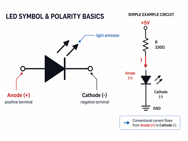
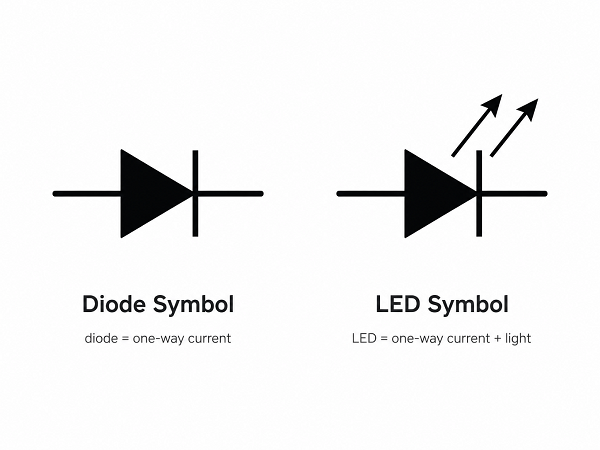
The symbol for an LED is a diode symbol with two arrows pointing away from it. The diode part shows that current flows mainly in one direction, while the outward arrows show light emission.

In a schematic, the LED symbol usually has two sides:

LED Symbol PartMeaningPractical Note
AnodePositive sideCurrent enters here in normal operation
CathodeNegative sideUsually marked by the vertical line/bar side
Two outward arrowsLight outputThis separates LED from a normal diode
Diode bodyOne-way current behaviorLED will not work like a resistor

A simple way to remember it: LED = diode + light arrows.

In circuit diagrams, the LED is often labeled as D, LED, LED1, D1, or sometimes LD. The exact reference designator depends on the designer’s naming rule, but in most PCB documentation, LED components are grouped with diodes because they are part of the diode family.

LED Symbol on PCB

The LED symbol on PCB is usually printed on the silkscreen layer to help assembly workers place the LED in the correct direction. It may appear as a diode symbol, a small outline with a flat side, a “+” mark, a “K” mark, or a cathode bar.

A schematic symbol tells the electrical function. A PCB footprint tells the physical placement. They must match.

Common PCB LED polarity marks include:

PCB MarkingWhat It Usually MeansReliability of Marking
“+” markAnode / positive sideVery clear when used correctly
“K” markCathode sideK comes from “Kathode”
Bar lineCathode sideCommon in diode-style markings
Flat side on outlineCathode side for many through-hole LEDsUseful but package-dependent
Square padOften pin 1, but not always polarityMust check library rule
Dot or chamferPin 1 or cathode/anode depending packageConfirm with datasheet

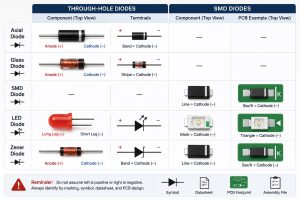
For through-hole LEDs, the PCB may show a circular outline with one flat edge. This flat edge normally matches the flat side of the LED body, which is commonly the cathode. For SMD LEDs, the polarity mark is often a tiny notch, dot, bevel, green mark, or printed line on the package.

The most common mistake is assuming every PCB library uses the same polarity convention. In real production, this is risky. Some CAD libraries mark pin 1, while the LED datasheet may define pin 1 as cathode or anode depending on the package. Before release, the schematic symbol, PCB footprint, assembly drawing, pick-and-place file, and BOM should all be checked together.

Which Side of the LED Symbol Is Positive?

The positive side of the LED symbol is the anode. In the standard diode-style symbol, the anode is on the side without the vertical bar, and the cathode is on the side with the bar.

The easiest rule is:

Anode = positive side
Cathode = negative side
Cathode side = bar side in the symbol

led symbol on pcb

In normal operation, conventional current flows from the anode to the cathode. That is why the LED only lights when it is forward-biased. If the anode is connected to a higher potential and the cathode is connected through the correct current-limiting path to a lower potential, the LED can turn on.

For real components, polarity can be checked in several ways:

LED TypePositive Side ClueNegative Side Clue
Through-hole LEDLonger lead is usually anodeShorter lead is usually cathode
Round through-hole LEDSmaller internal electrode often anodeLarger internal electrode often cathode
SMD LEDDatasheet defines anode markPackage mark often identifies cathode
PCB footprint“+” often marks anodeBar or “K” often marks cathode

Main Types of LED Symbols and Related Diode Symbols

The LED symbol belongs to the diode symbol family. Different diode types use similar base shapes, but each has extra marks that show its function.

Symbol TypeVisual FeatureMeaningCommon PCB Use
Standard diodeDiode body with barOne-way current flowRectification, reverse protection
LEDDiode body with two arrows pointing outwardEmits lightIndicators, displays, optocouplers, lighting
PhotodiodeDiode body with arrows pointing inwardDetects lightSensors, optical receivers
Zener diodeDiode symbol with bent cathode lineVoltage regulation/clampingReference, surge protection
Schottky diodeModified cathode markingLow forward voltage, fast switchingPower conversion, reverse protection
TVS diodeSuppression-style diode symbolTransient protectionESD and surge protection
Laser diodeLED-like symbol, often with laser indicationCoherent light outputOptical modules, sensors

LED and photodiode symbols are often confused by beginners. The difference is direction of arrows. LED arrows point outward because light leaves the device. Photodiode arrows point inward because light enters the device.

On PCB silkscreen, not every diode type is printed with a full symbol. Some boards use short polarity marks only. For compact boards, especially HDI, wearable electronics, medical modules, and LED driver PCBs, there may be limited space for full silkscreen. In that case, the assembly drawing and component datasheet become even more important.

Which Symbol Is Correct for an LED?

The correct symbol for an LED is a diode symbol with two arrows pointing outward. A plain diode symbol is not technically wrong for showing one-way conduction, but it does not communicate the light-emitting function.

For professional schematics, the LED should use the dedicated LED symbol. This makes the circuit easier to read for engineers, technicians, purchasing teams, and assembly houses.

A correct LED symbol should show:

  • The diode direction
  • The cathode bar
  • The light-emission arrows
  • The reference designator, such as LED1 or D3
  • The value or color, when needed
  • The package or part number in the BOM

For example, an indicator LED might be labeled:

LED1, Green, 0603, 2.0V typical Vf, 20mA max

For a high-power LED, the documentation should be more detailed. It may include forward voltage range, rated current, luminous flux bin, color temperature, thermal pad requirements, and recommended soldering profile.

The symbol alone is not enough for manufacturing. It tells function and polarity, but the PCB assembler also needs the footprint, BOM, polarity mark, and placement data. A clean schematic symbol with a poor footprint can still cause assembly defects.

Which Symbol Is Correct for an LED?

How to Identify LED?

You can identify an LED by checking the package shape, polarity marks, component label, datasheet, and diode-test behavior with a multimeter. For PCB assembly, the datasheet and BOM should always be the final reference.

Common LED identification methods:

MethodHow It WorksBest Use
Look at the circuit symbolLED symbol has outward arrowsReading schematic diagrams
Check PCB silkscreenFind “LED,” “D,” “+,” “K,” or cathode barBoard inspection
Inspect the LED bodyFlat side or short lead often marks cathodeThrough-hole LED identification
Use a multimeter diode modeLED may glow faintly in forward directionBench testing
Check datasheetConfirms pinout, polarity, package, voltageProduction and procurement
Compare BOM and placement fileConfirms exact part usedSMT assembly

For through-hole LEDs, identification is usually simple. The longer leg is commonly positive, and the shorter leg is commonly negative. The flat side on the plastic lens often marks the cathode.

For SMD LEDs, visual identification can be harder. Some packages have a tiny green line, a beveled corner, a dot, or a T-shaped mark. But different manufacturers use different conventions. One 0603 LED may mark the cathode; another may mark the anode. That is why datasheet checking is not optional for mass production.

In PCB manufacturing, a good LED identification process includes component verification before assembly, first article inspection after SMT, and polarity confirmation during AOI or manual inspection. For LED lighting products, additional functional testing is usually needed because a visually correct component can still have color bin, brightness, or forward voltage mismatch issues.

What Is the Element Symbol for LED?

LED does not have a chemical element symbol because it is not a single element. LED stands for Light Emitting Diode, which is an electronic component made from semiconductor materials.

This question often appears because “symbol” can mean two different things:

TermMeaning
LED symbolSchematic symbol used in circuit diagrams
Element symbolChemical abbreviation, such as Cu for copper or Si for silicon
Reference designatorPCB label, such as LED1, D2, or D5
Package markingPhysical mark printed on the LED component

An LED can contain materials such as gallium arsenide, gallium phosphide, gallium nitride, indium gallium nitride, or aluminum gallium indium phosphide, depending on color and performance. But the component itself is not represented by one chemical element symbol.

In schematic and PCB documentation, the more useful identifiers are the circuit symbol, reference designator, manufacturer part number, and package footprint. For procurement, the part number matters more than the generic name. For assembly, the footprint and polarity mark matter more than the visual symbol alone.

How to Tell Which LED Wire Is Positive?

For a typical through-hole LED, the longer wire is the positive side, also called the anode. The shorter wire is the negative side, also called the cathode.

You can also check the LED body. Many round LEDs have a flat side on the rim. That flat side usually marks the cathode. Inside the transparent lens, the larger metal cup is usually the cathode, while the smaller internal electrode is often the anode.

Here is a practical checklist:

ClueUsually Indicates
Longer leadAnode / positive
Shorter leadCathode / negative
Flat side on LED bodyCathode / negative
Larger internal metal cupCathode / negative
PCB “+” markAnode / positive
PCB bar or “K”Cathode / negative

For new parts, these rules work well most of the time. For trimmed leads, recycled parts, custom LEDs, or already-mounted components, use a multimeter in diode mode. Connect the red probe to one lead and the black probe to the other. If the LED glows faintly or shows a forward voltage reading, the red probe is on the anode and the black probe is on the cathode.

Never test a bare LED directly with a high-current power supply unless you use a current-limiting resistor or a controlled LED tester. LEDs are current-driven devices. Too much current can damage the junction quickly.

What Happens If You Wire a LED Light Backwards?

If you wire an LED backwards, it will usually not light because it is reverse-biased. In low-voltage circuits, it may simply stay off. In higher-voltage or poorly protected circuits, reverse bias can damage the LED.

The result depends on the circuit:

SituationLikely Result
Low voltage with current limitLED does not light
Reverse voltage above LED ratingLED may break down
No current-limiting resistorLED may fail when corrected or during fault
LED array wired incorrectlyOne LED may stop an entire string
High-power LED on MCPCBHeat and electrical stress may cause early failure
Reverse polarity in finished PCBAFunctional test failure or field return

Many small indicator LEDs have a limited reverse voltage rating, often around a few volts depending on the datasheet. Once reverse stress exceeds the rating, leakage current can increase and the LED junction may degrade. The component may not fail immediately, but its brightness, stability, or service life can be affected.

For PCB designers, reverse polarity risk can be reduced by adding clear silkscreen marks, using keyed connectors, checking schematic-to-footprint mapping, and including polarity inspection in the assembly process. For LED driver boards, protection design is also important, especially when connectors may be installed by end users.

What Is the Difference Between LED and LCD?

LED and LCD are different technologies. An LED emits light directly, while an LCD controls light but usually needs a backlight to be visible.

ItemLEDLCD
Full nameLight Emitting DiodeLiquid Crystal Display
Basic functionEmits lightControls light transmission
Needs backlight?No for a single LED indicatorUsually yes
PCB roleIndicator, lighting source, display segment, backlightDisplay module with driver circuit
PolarityYes, LED is polarizedLCD module has pin orientation and power requirements
Common usePower indicator, status light, lamps, displaysScreens, meters, panels, instruments

In everyday language, “LED display” and “LCD display” are sometimes used loosely. Many so-called LED TVs are actually LCD panels with LED backlighting. The LED is the light source, while the LCD panel forms the image.

On a PCB, an LED is normally treated as a diode component. An LCD is usually treated as a display module or connectorized assembly. It may include driver ICs, backlight LEDs, flexible cables, zebra connectors, or surface-mounted connectors. Their schematic symbols, footprints, BOM requirements, and inspection methods are different.

LED Symbol and PCB Polarity Design Tips

A correct LED circuit is not only about the schematic symbol. The PCB footprint, silkscreen, copper layout, resistor placement, and assembly documents must all support the same polarity rule.

For indicator LEDs, place the current-limiting resistor close enough to make the circuit easy to follow. For dense PCBs, keep the LED reference designator visible whenever possible. If the board has many LEDs in an array, use consistent orientation so inspection is faster.

For production-ready PCB files, check these points before release:

Design ItemGood PracticeWhy It Matters
Schematic symbolUse true LED symbol with cathode barAvoids confusion with normal diode
Footprint polarityMatch datasheet pinoutPrevents reversed placement
SilkscreenMark “+,” “K,” bar, or flat side clearlyHelps manual and visual inspection
BOMInclude exact manufacturer part numberAvoids color/package mismatch
Pick-and-place fileCorrect rotation and centroidReduces SMT placement errors
Assembly drawingShow polarity for LED partsSupports first article inspection
Test planInclude LED function testCatches reversed or wrong-color LEDs

For SMD LEDs, rotation is a common production issue. A footprint may look symmetric, but the LED is electrically polarized. If the centroid file uses a different zero-degree orientation from the assembler’s machine library, the LED can be rotated incorrectly. This is why first article inspection is important before full production.

Common LED Symbol and Assembly Mistakes

LED-related PCB mistakes are often small, but they can create visible product defects. A reversed resistor may not matter, but a reversed LED usually matters immediately.

Common mistakes include:

MistakeCauseResultPrevention
Reversed LED footprintSymbol pin mapping does not match packageLED does not lightCompare schematic, footprint, and datasheet
Wrong silkscreen mark“+” placed on wrong padAssembly confusionReview polarity on assembly drawing
Missing current-limiting resistorLED connected directly to supplyLED burnoutCalculate resistor or use LED driver
Wrong LED colorBOM not specific enoughVisual mismatchInclude part number, wavelength, CCT, bin
Incorrect SMD rotationPlacement angle mismatchBatch failure riskConfirm first article before mass run
Weak thermal pathHigh-power LED on poor copper designBrightness decay, heat damageUse MCPCB, copper core PCB, or thermal vias as needed
No functional testVisual inspection onlyHidden polarity or brightness issueAdd power-on LED test

For high-power LED PCB design, thermal management becomes part of electrical reliability. The symbol may look simple, but the PCB structure may need aluminum PCB, copper core PCB, heavy copper copper paths, thermal vias, or direct thermal pad design. LED lifetime is strongly affected by junction temperature, so layout and material choice should not be treated as secondary details.

For small signal LEDs, the most useful improvement is documentation clarity. A clean polarity mark can save hours of troubleshooting in prototypes and reduce assembly questions in volume production.

LED Symbol in Real PCB and PCBA Projects

In real projects, the LED symbol appears in many more places than simple breadboard circuits. It is used in consumer electronics, medical devices, industrial controllers, automotive dashboards, communication equipment, power supplies, IoT products, LED lighting, and test fixtures.

Typical LED use cases include:

ApplicationLED FunctionPCB Design Concern
Power supply boardPower-on indicatorResistor value, visibility, polarity
Industrial controllerStatus signalLabel clarity, EMI environment, serviceability
Medical device PCBAAlarm or state indicationReliability, color consistency, inspection
Automotive switch panelBacklight or indicatorTemperature, vibration, lifetime
LED lighting boardMain light sourceThermal path, current control, material choice
Communication equipmentPort status LEDPlacement accuracy, light pipe alignment
Test fixtureDebug indicatorEasy probing and replacement

In a prototype, an LED is often used as a quick debugging tool. Engineers may add LEDs to show power rails, MCU status, communication activity, charging state, or fault conditions. In production, those LEDs must be reviewed carefully. Debug LEDs may increase cost, power consumption, assembly time, or light leakage. Some are removed before mass production, while others are kept for service diagnostics.

For PCB buyers, LED-related details should be included in the quotation package when they affect assembly. The Gerber file alone may show pads and silkscreen, but it does not confirm the exact LED color, brightness, viewing angle, polarity mark, packaging reel direction, or test requirements.

How to Prepare LED PCB Files for Manufacturing

For LED PCB or PCBA production, clear files reduce quotation delays and assembly risk. The manufacturer should not need to guess LED polarity from a blurry image or incomplete BOM.

A strong file package should include:

  • Gerber files
  • Drill files
  • BOM with manufacturer part numbers
  • Pick-and-place file
  • Assembly drawing
  • Schematic PDF
  • LED datasheets
  • Polarity notes for SMD LEDs
  • Test requirements
  • Lighting performance requirements, if applicable

For LED lighting projects, also provide thermal requirements such as input power, LED current, operating temperature, target lifetime, board material, copper thickness, and heat sink information. For indicator LED projects, provide color, package size, brightness range, and lens or enclosure alignment requirements.

Best Technology supports standard FR4 PCB, multilayer PCB, metal core PCB, ceramic PCB, flexible and rigid-flex PCB, high-frequency PCB, PCB assembly, and component sourcing. The company also lists quality certifications including IATF 16949, ISO 9001:2015, ISO 13485:2016, AS9100D, REACH, RoHS, and UL.

FAQs

What Does the LED Symbol Look Like?

The LED symbol looks like a diode symbol with two small arrows pointing outward. The diode part shows one-way current flow, and the arrows show light emission. The vertical bar side is the cathode, while the other side is the anode. This symbol is used in schematics to separate LEDs from standard diodes, Zener diodes, and photodiodes.

What Does LED Mean in Electronics?

LED means Light Emitting Diode. It is a semiconductor component that emits light when current flows through it in the forward direction. Because it is a diode, it has polarity. The positive side is called the anode, and the negative side is called the cathode. It is widely used for indicators, displays, backlighting, and lighting systems.

Is the Arrow on an LED Symbol the Current Direction?

The diode body in the LED symbol shows the normal forward direction from anode to cathode for conventional current. The two small arrows pointing away from the symbol do not show current direction. They show emitted light. This is an important distinction because beginners sometimes read the light arrows as electrical direction, which can lead to wrong polarity decisions.

Which Side Is Negative on an LED Symbol?

The negative side of an LED symbol is the cathode. In the standard symbol, the cathode is the side with the vertical bar. On a PCB, the cathode may be marked with a bar, “K,” flat side, dot, or package mark. For mass production, always check the LED datasheet and the PCB footprint pin mapping.

Does the Flat Side of an LED Mean Negative?

For many round through-hole LEDs, the flat side of the plastic body marks the negative side, or cathode. The shorter lead also usually marks the cathode. However, this rule should be used with care for special LEDs, trimmed leads, and SMD packages. For production, the datasheet is more reliable than visual inspection alone.

Can an LED Work Without a Resistor?

An LED should not be connected directly to a voltage source unless the circuit already includes current control. A resistor or LED driver is normally used to limit current. Without current limiting, the LED may draw too much current and fail. The resistor value depends on supply voltage, LED forward voltage, and target current.

Why Does My LED Not Light on the PCB?

The LED may not light because it is reversed, the resistor value is too high, the supply voltage is missing, the solder joint is poor, the LED is damaged, or the wrong part was assembled. Start by checking polarity, forward voltage, current path, and solder quality. Then compare the schematic, PCB footprint, BOM, and datasheet.

How Do I Test LED Polarity With a Multimeter?

Set the multimeter to diode mode. Touch the red probe to one LED lead and the black probe to the other. If the LED glows faintly or shows a forward voltage reading, the red probe is on the anode and the black probe is on the cathode. If it does not respond, reverse the probes and test again.

Is LED an AC or DC Component?

An LED is normally driven by DC current in the forward direction. It can be used in AC circuits only with proper protection, rectification, or current limiting. Direct reverse voltage from AC can damage an LED if it exceeds the rated limit. LED lamps for AC mains include driver circuits, not just bare LEDs.

What Is the Difference Between Anode and Cathode in an LED?

The anode is the positive side of the LED during normal forward operation. The cathode is the negative side. Current flows from anode to cathode, and the LED emits light when the forward voltage and current are suitable. On the schematic symbol, the cathode is usually shown by the vertical bar.

Why Are LED Symbols Printed on PCB Silkscreen?

LED symbols or polarity marks are printed on PCB silkscreen to guide assembly and inspection. Since LEDs are polarized, the assembler must know which pad is anode and which pad is cathode. Clear silkscreen helps prevent reversed placement, especially during manual soldering, prototype builds, rework, and first article inspection.

Are All SMD LED Polarity Marks the Same?

No. SMD LED polarity marks vary by manufacturer and package. Some marks indicate the cathode, while others may indicate the anode or pin 1. The mark may be a dot, line, notch, bevel, or colored area. For SMT production, the datasheet and confirmed pick-and-place orientation are essential.

What Does K Mean on an LED PCB Footprint?

“K” usually means cathode. It comes from the German word “Kathode.” If a PCB footprint has a “K” mark beside one pad, that pad should connect to the negative side of the LED in normal operation. Even so, it is good practice to compare the footprint with the schematic and LED datasheet.

Can a Reversed LED Damage a Circuit?

A reversed LED often just stays off in low-voltage circuits. However, if the reverse voltage is too high or the circuit has poor current protection, the LED can fail. In LED strings, one reversed LED can stop the entire string from lighting. In finished products, reversed LEDs usually cause functional test failure.

What Should I Send to a PCB Manufacturer for LED Assembly?

Send Gerber files, BOM, pick-and-place file, assembly drawing, schematic PDF, LED datasheets, polarity notes, and test requirements. For high-power LED boards, also provide current, power, thermal requirements, board material preference, copper thickness, and operating environment. Clear documentation helps reduce assembly errors and quotation delays.

Conclusion

The LED symbol is simple, but its manufacturing meaning is important. It shows a polarized light-emitting diode, with the anode as the positive side and the cathode as the bar side. On a PCB, that symbol must match the footprint, silkscreen, BOM, datasheet, and placement file.

For design and purchasing teams, the safest approach is to treat LED polarity as a controlled assembly detail, not a visual guess. Check the schematic-to-footprint mapping, confirm SMD polarity marks, use current limiting, and include LED function testing when the product depends on visible status or lighting performance.

If you’re sourcing reliable PCB/PCBA manufacturing — OEM, ODM, prototyping, mass production, or custom engineering solutions — reach out to our engineering team for technical support and a quote at sales@bestpcbs.com.

You may also like

Do ceramic capacitors have polarity? Ceramic smd capacitor polarity

June 26th, 2026

Do ceramic capacitors have polarity? In most cases, ceramic capacitors do not have polarity. A standard ceramic disc capacitor, multilayer ceramic capacitor, or ceramic SMD capacitor is a non polarized ceramic capacitor. It does not have a fixed positive or negative terminal, so it can usually be installed in either direction. This is different from aluminum electrolytic capacitors and tantalum capacitors, which normally require correct polarity during PCB assembly.

Do ceramic capacitors have polarity? Ceramic smd capacitor polarity

However, the answer should not stop at “yes” or “no.” In real PCB design and PCBA production, engineers still need to confirm the capacitor type, value, voltage rating, dielectric material, package size, and assembly data. A ceramic capacitor may not need polarity control, but it still needs correct selection and accurate placement. Wrong capacitance, wrong voltage rating, or wrong package can still affect circuit performance.

Does ceramic capacitor have polarity?

A standard ceramic capacitor does not have polarity. It has two terminals, but neither terminal is permanently positive or negative. In most circuits, either side can be connected to the higher voltage node or the lower voltage node, as long as the capacitor is used within its rated electrical conditions.

This applies to most ceramic disc capacitors and multilayer ceramic capacitors, often called MLCCs. These capacitors use ceramic material as the dielectric between conductive electrodes. The dielectric structure does not depend on a chemically formed positive or negative layer, so the part can work with voltage applied in either direction.

For ceramic SMD capacitor polarity, the rule is the same. Common SMD ceramic capacitors in packages such as 0402, 0603, 0805, 1206, and 1210 are normally non-polarized. During SMT assembly, they do not need to be placed according to a positive or negative terminal.

This feature is useful in PCB layout. Designers can place ceramic capacitors in the shortest and most effective path, especially near IC power pins. For decoupling and bypassing, close placement is often more important than visual orientation. A 100 nF ceramic capacitor near a microcontroller, power management IC, memory chip, or RF module can usually face either direction without changing its basic function.

Still, “no polarity” does not mean the capacitor can be used without limits. The voltage rating must fit the circuit. The capacitance tolerance must match the design target. The dielectric class, such as C0G/NP0, X7R, X5R, or Y5V, should be selected according to stability, temperature range, DC bias behavior, and application requirements. The PCB footprint must also match the package.

So, does ceramic capacitor have polarity? For normal ceramic disc capacitors and ceramic SMD capacitors, the answer is no. They are non-polarized components. The main engineering task is not to identify positive and negative terminals, but to confirm that the capacitor specification is suitable for the circuit.

How to tell if a capacitor has polarity?

You can tell whether a capacitor has polarity by checking its body marking, package style, schematic symbol, BOM description, and datasheet. Polarized capacitors usually have a clear indication for the positive or negative terminal. Non-polarized capacitors usually do not have polarity marks.

Aluminum electrolytic capacitors are the most common polarized capacitors. A through-hole aluminum electrolytic capacitor often has a stripe on the body to mark the negative side. Before trimming, the longer lead usually indicates the positive terminal. SMD aluminum electrolytic capacitors may use a printed mark, a colored region, or a top-side polarity sign to show orientation.

Do ceramic capacitors have polarity? Ceramic smd capacitor polarity

Tantalum capacitors are also polarized, but their marking style is different from many aluminum electrolytic capacitors. A tantalum capacitor often marks the positive side. This difference is important because assuming that all stripes indicate the same terminal can cause assembly errors.

Ceramic capacitors are different. A ceramic disc capacitor usually has two leads with no positive or negative mark. A ceramic SMD capacitor usually looks like a small rectangular chip with metal terminations on both ends. Most small MLCCs have no printed text or polarity sign. Their value and specification are confirmed through the reel label, BOM, part number, and datasheet.

Capacitor TypePolarityCommon MarkingTypical Use
Ceramic disc capacitorNoValue code, usually no polarity markFiltering, coupling, general circuits
Ceramic SMD capacitor / MLCCNoUsually no body marking on small sizesDecoupling, bypassing, RF, digital circuits
Aluminum electrolytic capacitorYesNegative stripe or PCB positive markBulk filtering, power smoothing
Tantalum capacitorYesOften positive-side markingCompact power filtering
Film capacitorUsually noValue and voltage markingAC coupling, audio, EMI circuits
SupercapacitorUsually yesPositive and negative marksBackup power, energy storage

The safest method is to check the BOM and manufacturer part number. For example, a BOM line that says “CAP CER 100nF 50V X7R 0603” describes a ceramic SMD capacitor and normally has no polarity. A BOM line that says “CAP ALUM 100µF 25V” describes an aluminum electrolytic capacitor, which normally requires polarity control.

The schematic can also help. Non-polarized capacitors are often shown as two equal parallel plates. Polarized capacitors may include a plus sign or a curved plate. PCB silkscreen may also show polarity marks for polarized capacitors. Since library symbols and footprint styles can vary, the datasheet should be treated as the final reference when there is any doubt.

In PCBA production, EBest Circuit recommends using complete BOM data, including capacitance, voltage rating, tolerance, dielectric type, package, manufacturer part number, and polarity notes when needed.

How to determine polarity of ceramic capacitor?

For a normal ceramic capacitor, there is no polarity to determine. The correct question is whether the component is truly a ceramic capacitor. Once the part is confirmed as a standard two-terminal ceramic capacitor, it can usually be installed in either direction.

Ceramic capacitor polarity identification should begin with the BOM. Descriptions such as “ceramic,” “MLCC,” “multilayer ceramic,” “C0G,” “NP0,” “X7R,” “X5R,” and “Y5V” usually indicate a non polarized ceramic capacitor. Descriptions such as “aluminum electrolytic,” “tantalum,” “polymer,” or “supercapacitor” suggest that polarity may apply.

For through-hole ceramic disc capacitors, printed codes such as 104, 103, 471, or 222 usually refer to capacitance value. For example, 104 means 100,000 pF, which equals 0.1 µF. These printed numbers are not polarity marks. If the capacitor is a standard ceramic disc type, either lead can normally go into either pad.

Do ceramic capacitors have polarity? Ceramic smd capacitor polarity

For ceramic SMD capacitors, there is often no printing on the component body. Small MLCCs are identified through packaging labels, reel information, purchase records, and assembly documentation. During manufacturing, the pick-and-place file may define a rotation angle, but this does not mean the capacitor has polarity. It simply tells the machine how to pick and place the part consistently.

A practical verification process can include the following steps:

  • Check the BOM description and manufacturer part number.
  • Confirm the dielectric type and package from the datasheet.
  • Look for any polarity mark on the component body or PCB silkscreen.
  • Compare the schematic symbol with the PCB footprint.
  • Ask for engineering confirmation if the part description is unclear.

This process is useful because many SMD parts look similar after mounting. A ceramic capacitor, resistor, ferrite bead, small inductor, and certain protection components may have similar sizes. Reference designators help distinguish them. Capacitors are usually marked as C, resistors as R, inductors as L, and ferrite beads as FB or sometimes L depending on the company’s design standard.

What are the disadvantages of ceramic capacitors?

Ceramic capacitors have many practical advantages, including compact size, low ESR, good high-frequency behavior, and non-polarized installation. They are widely used for decoupling, bypassing, filtering, and signal coupling. At the same time, they have limitations that should be considered during design.

One important factor is DC bias. Many high-capacitance MLCCs lose part of their effective capacitance when DC voltage is applied. This effect is stronger in smaller package sizes and higher capacitance values.

Temperature behavior is another factor. C0G/NP0 ceramic capacitors are very stable across temperature and are often used in RF, timing, and precision circuits. X7R and X5R capacitors provide higher capacitance in smaller packages, but their capacitance changes more with temperature and voltage. This is not a defect. It simply means the dielectric type must match the circuit requirement.

Do ceramic capacitors have polarity? Ceramic smd capacitor polarity

Aging also matters for some ceramic dielectrics. Class 2 ceramic capacitors, such as X7R and X5R, can show capacitance reduction over time. For most decoupling applications, this is manageable when the design includes proper margin. For precision analog or timing circuits, a more stable dielectric such as C0G/NP0 is often preferred.

Mechanical stress should also be considered. MLCCs are made from hard ceramic material. Board bending, rough depaneling, connector insertion force, screw stress, or thermal shock may create cracks. Larger MLCC packages are more sensitive to board flex than smaller ones. In automotive, industrial, and high-reliability applications, soft termination MLCCs or improved layout placement may be used to reduce stress risk.

Ceramic capacitors may also produce acoustic noise in some power circuits. Under certain ripple conditions, MLCCs can vibrate due to piezoelectric behavior. This can create audible sound in products such as adapters, LED drivers, or compact power modules. Layout changes, package selection, voltage derating, or using a different capacitor type can help manage this issue.

Design FactorWhat It MeansEngineering Response
DC biasEffective capacitance may drop under working voltageCheck manufacturer DC bias curves and use voltage margin
Temperature coefficientCapacitance changes with dielectric typeUse C0G/NP0 for high stability; use X7R/X5R for compact capacitance
AgingSome dielectrics lose capacitance over timeAdd design margin for sensitive circuits
Mechanical stressCeramic body can crack under board flexAvoid high-stress areas; consider soft termination parts
Acoustic noiseMLCCs may vibrate in some power circuitsAdjust layout, package, voltage rating, or capacitor type
Limited bulk energy storageVery large capacitance may need other technologiesCombine ceramic with electrolytic or polymer capacitors when required

The right approach is to use ceramic capacitors where their characteristics fit the circuit. They are often suitable near IC power pins because they respond well at high frequencies. Electrolytic or polymer capacitors may be better for larger bulk capacitance. Film capacitors may be selected for certain AC, audio, or precision circuits.

For PCB and PCBA projects, EBest Circuit (Best Technology) reviews capacitor selection together with PCB layout, stack-up, soldering process, and product environment.

How Can You Tell If a Capacitor Is Ceramic?

You can often recognize a ceramic capacitor by its body shape, package, color, marking style, circuit position, and BOM description. Visual inspection helps, but the BOM and datasheet provide the most reliable confirmation.

A through-hole ceramic disc capacitor is usually a flat disc with two radial leads. The body may be orange, yellow, blue, brown, or light tan. It often has a printed capacitance code, such as 104, 103, 472, or 221. These codes identify value, not polarity. Standard ceramic disc capacitor polarity is not marked because the component is normally non-polarized.

A ceramic SMD capacitor is usually a small rectangular chip with metal end terminations. Common package sizes include 0201, 0402, 0603, 0805, 1206, and 1210. The body is often beige, cream, gray, or light brown. Many small MLCCs have no printed value because the surface area is too small.

Circuit location can also provide clues. Ceramic capacitors are often placed near IC power pins for decoupling. They may appear in groups around microcontrollers, FPGAs, memory ICs, RF chips, sensors, and power management ICs. In these locations, they help reduce high-frequency noise and stabilize local power delivery.

Common signs that a capacitor is ceramic include:

  • The BOM includes “ceramic,” “MLCC,” “C0G,” “NP0,” “X7R,” or “X5R.”
  • The part is a small rectangular SMD chip with no polarity mark.
  • The through-hole part has a disc-shaped body.
  • The schematic uses a non-polar capacitor symbol.
  • The component is placed near an IC power pin or in a filter network.

However, visual inspection alone can be misleading. Some resistors, ferrite beads, inductors, and small protection devices may look similar to ceramic capacitors. The reference designator gives an important clue. Capacitors are usually labeled C on the PCB and schematic. Resistors are labeled R, inductors are labeled L, and ferrite beads may be labeled FB.

Does polarity matter on a capacitor?

Polarity matters on some capacitors, but not on all capacitors. Whether polarity matters depends on the capacitor’s internal construction. A polarized capacitor must be installed in the correct direction. A non-polarized capacitor can be installed in either direction.

For ceramic capacitors, polarity usually does not matter. Most ceramic capacitors are non-polarized, so they can be used in DC circuits, AC circuits, coupling paths, decoupling networks, and filter circuits without positive and negative orientation. This is one reason ceramic capacitors are so common in PCB assembly.

For aluminum electrolytic capacitors, tantalum capacitors, polymer capacitors, and supercapacitors, polarity normally matters. These components have a defined positive and negative terminal. If they are installed incorrectly, the circuit may not work as intended, and the capacitor may be damaged. PCB footprints for polarized capacitors usually include orientation marks to guide assembly.

QuestionCeramic CapacitorAluminum Electrolytic CapacitorTantalum Capacitor
Does polarity matter?Usually noYesYes
Can it be installed either way?Usually yesNoNo
Common polarity markUsually noneNegative stripe or PCB plus markOften positive-side mark
Common useDecoupling, filtering, RF, couplingBulk filtering, power smoothingCompact power filtering
Main assembly checkValue, package, voltage, dielectricValue, package, voltage, polarityValue, package, voltage, polarity

In short, polarity does not usually matter for ceramic capacitors, but it matters for many electrolytic, tantalum, polymer, and supercapacitor parts.

Why do ceramic capacitors have no polarity?

Ceramic capacitors have no polarity because of their internal dielectric and electrode structure. They use ceramic material as the insulating dielectric between conductive electrodes. This structure can store charge with voltage applied in either direction, as long as the capacitor remains within its rated voltage and operating range.

This is different from aluminum electrolytic capacitors. An electrolytic capacitor uses an oxide layer formed on a specific electrode. That structure is designed to operate with a defined positive and negative direction. Ceramic capacitors do not rely on that same electrochemical structure, so they do not need a fixed terminal orientation.

Do ceramic capacitors have polarity? Ceramic smd capacitor polarity

A multilayer ceramic capacitor contains many thin ceramic layers and electrode layers stacked together. Alternate electrode layers connect to opposite end terminations. When voltage is applied, electric fields form across the ceramic dielectric layers. Because the two-terminal MLCC structure is generally symmetrical for normal use, either terminal can be connected to the higher voltage side.

Even though ceramic capacitors have no polarity, voltage rating still matters. A non-polar component can be connected in either direction, but it should not be used above its specified voltage. Engineers often apply voltage derating, especially in industrial, automotive, medical, and power electronics applications. This improves design margin and helps manage DC bias effects in MLCCs.

Which capacitor has no polarity?

Ceramic capacitors are the most common non-polarized capacitors used in PCB assembly, but they are not the only ones. Film capacitors, mica capacitors, many safety capacitors, and some special non-polar electrolytic capacitors also have no fixed polarity.

A non-polarized capacitor is useful when the circuit voltage may reverse direction or when the signal is AC. These capacitors are common in coupling circuits, filters, RF networks, timing circuits, audio paths, EMI suppression, and general decoupling.

Non-Polar Capacitor TypePolarityMain StrengthCommon Application
Ceramic capacitorNoSmall size, high-frequency performanceDecoupling, bypass, RF, filtering
Film capacitorNoStability and AC performanceAudio, power, EMI suppression
Mica capacitorNoHigh stabilityRF and precision circuits
Safety capacitorUsually noCertified safety useMains EMI filtering
Non-polar electrolytic capacitorNoHigher capacitance for AC useAudio crossover and special AC circuits

The choice depends on circuit requirements. A 100 nF ceramic capacitor is commonly used for IC decoupling. A film capacitor may be selected for AC coupling or EMI applications. A safety capacitor is required in line-related positions. A non-polar electrolytic capacitor may be used where higher capacitance is needed in an AC path.

For most PCB projects, ceramic capacitors are the first non-polar option engineers consider because they are compact, available, and compatible with SMT production. Still, the correct capacitor type should always be selected based on voltage, capacitance, frequency, tolerance, temperature, and reliability requirements.

Can a Ceramic Capacitor Be Installed in Either Direction?

Yes, a standard ceramic capacitor can be installed in either direction. This applies to most ceramic disc capacitors and ceramic SMD capacitors. Since they are non-polarized, rotating the component 180 degrees does not change its normal electrical function.

This feature simplifies both manual soldering and automated SMT assembly. A ceramic disc capacitor can usually be inserted into a through-hole footprint either way. A ceramic SMD capacitor can usually be placed without positive or negative orientation. The placement file may still define rotation for machine control, but that rotation is not usually related to capacitor polarity.

In repair work, this also makes replacement easier. If a technician replaces a standard MLCC or ceramic disc capacitor, the key points are value, voltage rating, package size, dielectric type, and solder quality. Direction is normally not the deciding factor.

However, the component must first be identified correctly. A part that looks similar may not be a ceramic capacitor. Tantalum capacitors, diodes, LEDs, TVS diodes, ferrite beads, and other small SMD components may require different handling. The safest approach is to check the reference designator, BOM, schematic, and datasheet before replacing or assembling parts.

Some special ceramic-based components may also have defined pin arrangements. Capacitor arrays, EMI filters, feedthrough capacitors, and integrated passive components should be checked through their datasheets. They may use ceramic materials, but they are not the same as a standard two-terminal MLCC.

In summary, most ceramic capacitors have no polarity and can be installed in either direction. Ceramic capacitor polarity identification mainly means confirming that the component is a standard ceramic capacitor and verifying its capacitance, voltage rating, dielectric, package, and application fit.

For PCB fabrication, SMT assembly, BOM review, component sourcing, and turnkey PCBA support, EBest Circuit (Best Technology) can help review these details before production. If you have a PCB or PCBA project that needs engineering support or quotation, contact sales@bestpcbs.com

You may also like

Schematics Meaning: How to Read Schematic Diagrams, Symbols, and Circuit Numbers

June 22nd, 2026

A schematic is a simplified technical drawing that shows how parts of a system connect and work together. In electronics, a schematic diagram uses standard symbols, lines, labels, and circuit numbers to explain an electrical circuit before it becomes a PCB layout, wiring harness, or finished product.

For engineers, technicians, buyers, and students, understanding schematics is a practical skill. A schematic helps you see the logic behind a circuit, identify components, trace signals, check power connections, and communicate design intent clearly. It is not only a drawing. It is the technical language behind electronic design, PCB manufacturing, troubleshooting, and assembly.

Schematics Meaning: How to Read Schematic Diagrams, Symbols, and Circuit Numbers

What Does Schematic Mean?

In electronics, a schematic shows components such as resistors, capacitors, ICs, connectors, diodes, transistors, switches, sensors, and power supplies. These parts are represented by symbols. Lines between the symbols represent electrical connections, also called nets.

For example, a PCB schematic may show that a microcontroller pin connects to a resistor, then to an LED, and finally to ground. The drawing may not show where those components sit on the actual circuit board. That job belongs to the PCB layout. The schematic focuses on circuit logic.

This is why a schematic is usually created before PCB layout. If the schematic is wrong, the PCB layout will also carry that mistake into production.

What Does Schematic Mean?

What Is a Schematic Also Known As?

A schematic is also known as a schematic diagram, circuit diagram, electrical schematic, electronic schematic, wiring schematic, or circuit schematic.

These names are often used in different situations:

TermCommon MeaningTypical Use
Schematic diagramGeneral technical drawing showing connections and functionsElectronics, machines, control systems
Circuit diagramElectronic or electrical circuit drawingPCB design, repair, education
Electrical schematicDrawing for electrical power, control, or wiring logicIndustrial panels, machines, building systems
Electronic schematicDrawing for electronic circuits using components and ICsPCB, embedded systems, consumer electronics
Wiring schematicDrawing focused on wire connectionsAutomotive, equipment wiring, cable harnesses
Block diagramHigh-level system diagram using functional blocksEarly design, product architecture

In PCB work, “schematic” usually means the electronic circuit drawing used to generate the netlist for PCB layout. It is closely linked with the BOM, component footprints, design rules, and assembly documentation.

Electrical Schematic Symbols and Meanings

Electrical schematic symbols are standardized graphic marks used to represent components and functions. They help people read a circuit without needing a realistic picture of each part.

A resistor symbol does not look like an actual resistor body. A capacitor symbol does not show its real package size. An IC symbol may only show pin names and numbers. This simplified style makes the drawing easier to read, especially for complex circuits.

Here are common electrical schematic symbols and their meanings:

Component or Symbol NameMeaning in a SchematicCommon Reference Designator
ResistorLimits current, divides voltage, sets bias, or provides pull-up/pull-down controlR
CapacitorStores charge, filters noise, stabilizes voltage, or couples signalsC
InductorStores energy in a magnetic field, filters current, or works in power circuitsL
DiodeAllows current flow mainly in one directionD
LEDEmits light when current flows in the forward directionLED or D
Zener diodeProvides voltage regulation or overvoltage protectionZD or D
TransistorSwitches or amplifies signalsQ
MOSFETSwitches power or controls current flowQ
Integrated circuitPerforms logic, control, power conversion, memory, or signal processingU or IC
ConnectorProvides an interface to cables, modules, power, or external systemsJ, CN, or P
SwitchOpens or closes a circuit pathSW or S
FuseProtects a circuit by opening under excessive currentF
GroundCommon reference point for voltage and return currentGND
Power symbolShows supply voltage such as 3.3V, 5V, 12V, or VCCVCC, VIN, VDD
Test pointPlace for measurement during debugging or production testingTP
Crystal or oscillatorProvides a clock signal for ICs or microcontrollersY or X
Electrical Schematic Symbols and Meanings

Symbols may vary slightly depending on the standard, software, region, or industry. For PCB projects, the symbol must also match the correct footprint. A correct schematic symbol with the wrong footprint can still cause assembly failure.

For example, a capacitor may be electrically correct in the schematic, but if its footprint does not match the real package, the part may not fit during SMT assembly. This is a common DFM issue in PCB manufacturing.

What Do the Circuit Numbers Shown on Schematics Usually Mean?

The circuit numbers shown on schematics usually identify components, pins, wires, nets, pages, and functional sections. They help engineers, assemblers, and repair technicians locate the same item across the schematic, PCB layout, BOM, silkscreen, and test documents.

The most common numbers are reference designators. Examples include R1, R2, C1, U3, D5, J1, and TP2.

Here is what they usually mean:

ExampleMeaning
R15The fifteenth resistor listed in the design
C8The eighth capacitor listed in the design
U2The second IC or module listed in the design
D3The third diode or LED listed in the design
J1The first connector listed in the design
TP5The fifth test point listed in the design
Pin 1, Pin 2Physical or logical pin numbers on a component
Net labels such as SDA, SCL, GNDNames of electrical connections
Sheet numbersPage references in multi-page schematics

These numbers are important because they connect the design file to real production work. When a BOM says “R15 = 10kΩ, 1%, 0603,” the assembly team knows exactly which resistor to place at R15 on the PCB. When a technician checks a failed board and sees U2 overheating, the schematic helps identify what U2 does and which power rail feeds it.

What Is an Example of a Schematic?

A simple example of a schematic is an LED indicator circuit. In this circuit, a power source connects to a resistor. The resistor connects to an LED. The LED connects to ground. When voltage is applied, current flows through the resistor and LED, so the LED lights up.

The schematic may include:

  • VCC or 5V power symbol
  • R1 resistor
  • D1 LED
  • GND symbol
  • Connection lines between them
Example of a Schematic

In PCB manufacturing, this schematic later becomes part of the full design package. The PCB factory mainly uses Gerber files, drill files, stack-up, BOM, Pick-and-Place files, and assembly drawings, but the schematic is still valuable during engineering review, functional discussion, debugging, and DFM checks.

What Are the Two Types of Schematics?

There is no single universal answer because different industries classify schematics in different ways. In electronics and electrical engineering, two common types are electrical schematics and electronic schematics.

An electrical schematic often focuses on power distribution, control circuits, motors, relays, switches, breakers, terminals, and wiring paths. It is common in industrial equipment, automation panels, HVAC systems, vehicles, and building electrical systems.

An electronic schematic focuses on electronic components such as ICs, resistors, capacitors, diodes, MOSFETs, sensors, oscillators, connectors, and signal networks. It is common in PCB design, embedded systems, medical electronics, consumer devices, automotive control modules, communication devices, and power electronics.

What Is the Difference Between Blueprints and Schematics?

Blueprints and schematics are both technical drawings, but they serve different purposes.

A blueprint usually shows physical construction details. It focuses on dimensions, location, shape, structure, installation, and building or manufacturing instructions. Blueprints are common in architecture, mechanical design, construction, and product fabrication.

A schematic shows functional relationships. It focuses on how parts connect and work together. In electronics, it shows the electrical logic of a circuit, not the final physical position of every component.

ItemBlueprintSchematic
Main purposeShows physical structure and dimensionsShows functional connections and circuit logic
Common industriesConstruction, architecture, mechanical designElectronics, electrical systems, automation
Level of physical detailHighUsually low
Shows actual size or scaleOften yesUsually no
Shows electrical logicNot usuallyYes
Used for PCB designLess commonEssential before PCB layout

For PCB projects, the closest equivalent to a blueprint is the PCB layout or fabrication drawing. It shows board dimensions, hole sizes, layer stack-up, copper layers, solder mask, silkscreen, and manufacturing details. The schematic, however, shows the circuit logic behind that board.

What Are Schematics Used For?

Schematics are used to design, explain, verify, repair, and manufacture electrical or electronic systems. They act as a shared technical language between engineers, technicians, manufacturers, and customers.

In electronics, schematics are used for:

  • Circuit design
  • PCB layout preparation
  • Component selection
  • BOM creation
  • Signal tracing
  • Power rail review
  • Design verification
  • Debugging and repair
  • Functional testing
  • Engineering communication
  • Product documentation
  • Manufacturing support

For PCB and PCBA projects, schematics help detect issues before production. For example, an engineer may review whether pull-up resistors are missing, whether decoupling capacitors are placed on the correct power pins, whether connector pinouts match the cable, or whether power nets are named clearly.

What Are Schematics Used For?

Who Uses Schematics?

Schematics are used by many people across the product lifecycle. The same drawing may support concept design, PCB layout, manufacturing, testing, repair, and product improvement.

Common users include:

Electrical engineers use schematics to design power, control, and signal circuits.

Electronics engineers use schematics to create PCB-based products, embedded systems, power supplies, sensor boards, and communication modules.

PCB layout engineers use schematics to generate netlists and route the PCB correctly.

Firmware engineers use schematics to understand microcontroller pins, communication buses, reset circuits, boot modes, and debugging interfaces.

Manufacturing engineers use schematics to check test points, assembly risks, and production test logic.

Repair technicians use schematics to trace faults, measure voltages, and identify failed parts.

Quality engineers use schematics during failure analysis and process improvement.

Procurement teams may not design the circuit, but they use schematic-related data to understand BOM risk, part alternatives, and supplier communication.

Students and hobbyists use schematics to learn circuits and build projects.

In professional PCB manufacturing, a schematic is not always enough for quotation or production. A complete package usually includes Gerber files, drill files, BOM, Pick-and-Place files, PCB stack-up, assembly drawings, impedance requirements, and testing requirements. Still, the schematic remains one of the most important documents for understanding the design.

What’s the Difference Between a Diagram and a Schematic?

A diagram is a broad term. It can mean any drawing that explains information visually. A schematic is a specific kind of diagram that uses symbols and connections to show how a system works.

All schematics are diagrams, but not all diagrams are schematics.

For example, a flowchart is a diagram. A product exploded view is a diagram. A wiring map is a diagram. A PCB layout image is also a diagram in a general sense. But an electronic schematic is more specific because it follows circuit logic and uses electrical symbols.

ItemDiagramSchematic
MeaningGeneral visual explanationSymbol-based functional drawing
ScopeBroadMore specific
Can show physical shapeYesUsually simplified
Uses technical symbolsSometimesUsually yes
Common examplesFlowchart, block diagram, layout, mapCircuit schematic, electrical schematic
Main goalExplain visuallyShow how parts connect and function

A diagram may help someone understand an idea. A schematic helps someone build, test, or repair a system.

For PCB design, the difference is important. A product diagram may show where the board fits inside a device. A PCB layout shows component placement and routing. A schematic shows the electrical relationships that make the product work.

FAQs About Schematics Meaning

What does schematics mean in simple words?

Schematics means technical drawings that show how parts of a system connect and work together. In electronics, schematics use symbols to represent components such as resistors, capacitors, ICs, switches, connectors, and power sources. The drawing does not focus on physical appearance. It focuses on function and connection.

What is the meaning of a schematic diagram?

A schematic diagram is a simplified drawing that explains the structure or logic of a circuit, machine, or system. In an electrical or electronic schematic, symbols represent components, and lines represent connections. It helps engineers and technicians understand how current, signals, or control functions move through the design.

Are schematic diagrams and circuit diagrams the same?

In electronics, the terms are often used in the same way. A circuit diagram is a type of schematic diagram that shows electronic or electrical connections. However, “schematic diagram” can be broader. It may also describe hydraulic, mechanical, pneumatic, or system-level drawings in other industries.

Why are schematic symbols important?

Schematic symbols make complex circuits easier to read. Instead of drawing real component shapes, the schematic uses standard symbols that engineers can recognize quickly. This saves space, improves clarity, and reduces misunderstanding. Symbols also help connect the schematic to the BOM, PCB layout, testing process, and repair work.

Do schematics show the real location of components?

Usually, no. A schematic shows electrical connections and circuit logic, not the actual physical placement of parts. The PCB layout shows real component locations, copper traces, vias, board outline, and layer structure. Both documents are needed, but they answer different questions.

What do R, C, U, D, and J mean on a schematic?

These letters are reference designators. R usually means resistor, C means capacitor, U means integrated circuit, D means diode, and J often means connector. The number after the letter identifies the specific part, such as R1, C5, U2, or J3. These labels help match the schematic, BOM, PCB silkscreen, and assembly files.

Can a PCB be made from a schematic only?

A schematic alone is usually not enough for PCB fabrication. The manufacturer needs Gerber files, drill files, board specifications, stack-up, copper thickness, surface finish, solder mask color, and other fabrication details. For PCBA, the BOM and Pick-and-Place file are also needed. The schematic is useful for understanding and checking the circuit.

What is the difference between a schematic and a wiring diagram?

A schematic focuses on circuit function and logical connections. A wiring diagram focuses more on real wire connections, terminals, harnesses, and installation paths. In electronics, schematics are common for PCB design. Wiring diagrams are more common in automotive systems, industrial control cabinets, machines, and field installation work.

How do beginners read a schematic?

Start by finding the power input, ground symbols, and main functional blocks. Then identify key components such as ICs, connectors, regulators, sensors, and switches. Follow net labels and signal names instead of only following lines. Read reference designators and component values carefully. For complex circuits, study one section at a time.

Why do PCB manufacturers sometimes need schematics?

PCB manufacturers may request schematics during engineering review, PCBA debugging, functional testing, or DFM discussion. The schematic helps explain design intent, signal flow, power rails, connector functions, and test points. It is especially useful for complex boards involving impedance control, power circuits, RF sections, mixed-signal design, or turnkey assembly.

Conclusion

For PCB and PCBA projects, a clear schematic reduces design errors, improves communication, supports better layout work, and makes testing or troubleshooting much easier. Before moving from design to manufacturing, it is worth checking that the schematic, BOM, footprints, net names, connector pinouts, and PCB layout all match correctly.

If you’re sourcing reliable PCB/PCBA manufacturing — OEM, ODM, prototyping, mass production, or custom engineering solutions — reach out to our engineering team for technical support and a quote at sales@bestpcbs.com

You may also like

Antenna PCB Connector Guide for Wireless PCB Assembly

June 18th, 2026

Wireless products depend on a stable RF path from the radio circuit to the antenna. An antenna PCB connector looks small, but it can affect signal range, impedance matching, cable reliability, assembly yield and final wireless testing. For WiFi, GSM, IoT, GPS, medical and industrial devices, connector choice should be reviewed together with the PCB layout, antenna cable, enclosure and production test plan.

Antenna PCB Connector, https://www.bestpcbs.com/blog/2026/06/antenna-pcb-connector/

What Is an Antenna PCB Connector in Wireless PCB Assembly?

An antenna PCB connector is a board-mounted RF interface that links a wireless circuit to an antenna, coaxial cable or RF test point. It carries high-frequency signals between the radio module, matching network and antenna system.

The core function is to maintain a controlled RF path, usually 50Ω, while giving the product a reliable mechanical connection. It may be a U.FL/I-PEX socket, SMA connector, MMCX connector, RF switch connector or board-edge coaxial launch.

In PCBA projects, this part is common in WiFi modules, GSM trackers, IoT gateways, GPS devices, smart meters, medical wireless devices and industrial controllers.

What Types of Antenna PCB Connectors Are Commonly Used?

Common antenna PCB connector types include SMA, RP-SMA, U.FL/I-PEX/MHF, MMCX, MCX, board-edge launch connectors and RF switch connectors. Each option fits a different balance of size, strength, frequency, cost and antenna structure.

For compact wireless PCBA, U.FL or MHF is common. For external antennas and repeated field mating, SMA or RP-SMA is usually safer. MMCX and MCX offer stronger snap-on retention than micro coax connectors while staying smaller than SMA.

TypeMountStrengthCommon Use
SMAThrough-hole / edge / panelHighRouters, gateways, test ports
RP-SMAThrough-hole / panelHighWiFi antennas, consumer wireless
U.FL / I-PEXSMTLow to mediumIoT, GPS, WiFi modules
MHF4 / MHF5SMTLowCompact 5G, M.2, wearable devices
MMCXSMT / through-holeMediumDrones, GPS, RF modules
MCXSMT / through-holeMediumRF equipment, test interfaces
RF switchSMTLowProduction test, diagnostics

What Are the Advantages and Limits of Antenna PCB Connector?

A connector gives the product flexibility, but it also adds a new RF and mechanical risk point. The benefit is strongest when the product uses external antennas, replaceable antenna cables or production RF test fixtures.

The advantage is design flexibility; the limit is added loss, cost and handling risk. A direct PCB antenna feed may be cheaper, while a connector-based design is easier to tune, test, service and adapt to different markets.

Advantages include:

  • External antenna options for weak-signal environments.
  • Easier WiFi, GSM, GPS or Bluetooth testing.
  • Flexible antenna cable routing inside the enclosure.
  • Faster product variants using one PCB platform.

Limits include:

  • Extra insertion loss in the RF path.
  • Higher BOM and assembly cost.
  • Limited mating life for micro connectors.
  • Risk of cable damage during PCBA testing.

SMA vs U.FL vs MMCX: Which PCB Antenna Connector Should You Choose?

Choose SMA for strength, U.FL for compact internal cables and MMCX when the product requires a small connector with better retention than U.FL. The right PCB antenna connector depends on enclosure access, mating cycles, vibration, board space and antenna position.

Use SMA for external access, U.FL for internal space saving and MMCX for compact products that still require stronger snap-on retention. This simple rule helps reduce selection errors during early design.

OptionSizeMating StyleAdvantageLimit
SMALargeThreadedStrong field connectionMore board and panel space
U.FLVery smallSnap-onSaves PCB spaceLimited mating cycles
MMCXSmallSnap-onBetter retention than U.FLHigher cost and larger footprint

For terms such as SMA-F male antenna PCB connector or SMA-female antenna PCB connector, confirm the exact drawing. SMA gender may describe the body, center contact or reverse-polarity version.

How Should You Select a WiFi Antenna Connector for PCB Assembly?

A WiFi antenna PCB connector should match the WiFi band, antenna cable, enclosure, wireless module and final test method. Modern WiFi devices may use 2.4 GHz, 5 GHz or 6 GHz, so the connector and coaxial cable must support the highest working band.

For routers and gateways, SMA or RP-SMA is practical for external antennas. For compact IoT devices, U.FL, I-PEX, MHF4 or MHF5 is usually preferred. In MIMO products, each RF path should follow the same impedance target and cable discipline.

Selection points:

  • Use 50Ω RF connectors and coaxial cable.
  • Keep the antenna cable short when space allows.
  • Confirm mating height and cable plug series.
  • Reserve space for cable bending and operator access.
  • Test with the final enclosure installed.

How Should GSM Antenna Connectors Be Chosen for Wireless PCB Projects?

A GSM antenna PCB connector should support cellular bands, antenna power level, coaxial cable routing and the mechanical environment. GSM, LTE, NB-IoT and Cat-M products often work across low and high cellular bands, so connector loss and antenna matching must be reviewed together.

For trackers, smart meters and industrial cellular devices, connector retention and cable strain relief matter as much as RF performance. U.FL is common inside compact devices, while SMA is better for external antennas mounted outside the housing.

Practical checks include:

  • Confirm all target bands before approving the connector.
  • Keep the feed path away from batteries, shields and metal frames.
  • Use cable support when the product may vibrate.
  • Review antenna gain, cable loss and connector loss together.
  • Run conducted and over-the-air tests before mass production.

What Type of Connectors Do You Need for PCB Antenna Designs?

The right connector depends on antenna type, board space, enclosure structure, frequency band and test method. Some PCB antenna designs use a direct RF feed, while others need a removable coaxial interface.

PCB antenna designs do not always require the same connector type, and the final choice should match the antenna structure and production test plan.

  • PCB trace antenna: Usually uses a direct feed from the matching network. An RF test connector may be added for tuning and validation.
  • Chip antenna: Often uses a direct feed with a strict keep-out area. The connector is mainly used for testing or alternative antenna versions.
  • Flexible antenna: Commonly uses U.FL, I-PEX, MHF4 or MHF5 because these connectors save PCB space and support internal cable routing.
  • External antenna: Usually uses SMA, RP-SMA, MMCX or MCX. These connectors are better for products that require stronger mating, external access or field replacement.
  • PCB antenna array connector: Used when multiple antenna paths require controlled coaxial feeds, consistent cable length and stable RF matching.
  • Compact IoT design: Micro coax connectors are suitable, but mating life, cable bending and assembly access must be checked early.
  • Industrial wireless design: SMA or MMCX is safer when the product faces vibration, repeated service or outdoor installation.

The final choice should balance 50Ω matching, antenna position, cable strain, enclosure space and production test reliability.

How to Add Antenna Connectors to a PCB During PCBA Assembly?

Adding antenna connectors to a PCB should be controlled from design review to final wireless testing. Most assembly problems come from wrong footprints, poor soldering, cable stress or uncontrolled mating force. A stable assembly process should confirm the connector footprint, RF layout, solder quality, cable mating method and final wireless test result.

Step 1: Review the connector datasheet, footprint, mated height, cable plug, impedance target and antenna type before PCB fabrication. Confirm that the land pattern matches the selected connector series.

Step 2: Check the RF layout before SMT production. The feed line, ground vias, keep-out area, matching network and cable exit direction should be reviewed together.

Step 3: Print solder paste with controlled volume. Micro RF connectors need accurate paste coverage because excessive solder can cause tilt, while insufficient solder can weaken retention.

Step 4: Place the connector by SMT machine with correct orientation and alignment. Manual correction should be avoided unless inspection rules are clear.

Step 5: Reflow the PCB with a verified temperature profile. The connector body, plastic insulator and solder pads must tolerate the process window.

Step 6: Inspect the connector after reflow. Use AOI, microscope inspection or manual visual inspection to check solder joints, shell position, pad wetting and connector flatness.

Step 7: Mate the antenna cable with controlled vertical force. Avoid angled pressing, twisting or pulling the cable near the connector.

Step 8: Add cable retention when required. Adhesive, foam, clips or enclosure support can reduce cable movement during vibration or final assembly.

Step 9: Run RF and wireless function tests before shipment. The connector should be checked as part of the full antenna system, not as an isolated component.

adding antenna connectors to a pcb, https://www.bestpcbs.com/blog/2026/06/antenna-pcb-connector/

What Layout Rules Matter for Antenna Connector PCB Design?

Antenna connector PCB design should protect the RF signal path from the wireless IC to the antenna. A correct footprint is not enough if the feed trace, ground return or antenna keep-out area is poorly designed.

Good layout reduces signal reflection, wireless range loss, connector stress and late-stage antenna tuning problems.

  • Keep the RF feed controlled at 50Ω. Use the correct trace width, dielectric thickness and ground reference based on the PCB stackup.
  • Place the matching network close to the antenna feed. This improves tuning control and reduces extra parasitic effects.
  • Keep the RF trace short and direct. Avoid unnecessary bends, stubs, vias and layer transitions.
  • Use solid ground reference under the RF path. Broken ground can increase impedance variation and signal loss.
  • Add ground vias near the connector. Dense via stitching helps create a stable return path around the connector launch area.
  • Reserve antenna keep-out space. Copper, metal shields, batteries and large components near the antenna can detune wireless performance.
  • Avoid routing noisy signals near the RF path. Switching power traces, clocks and high-current lines can introduce interference.
  • Control cable exit direction. The antenna cable should leave the connector without sharp bending or pressure from the enclosure.
  • Check mechanical clearance. The connector must have enough space for mating tools, cable bending and final assembly.
  • Validate with the final enclosure. Plastic walls, metal coating, screws and batteries can change RF performance after assembly.

How Does Connector Placement Affect Wireless Signal Performance?

Connector placement affects wireless performance because the RF feed, antenna cable and enclosure create one working system. A connector placed near metal, batteries, displays, motors or switching power circuits can increase loss or detune the antenna.

Place the antenna feed area near a PCB edge or corner when the antenna requires open space. Keep the cable path free from sharp bends, cover pressure and moving parts.

For MIMO WiFi, LTE diversity or antenna array products, separate antenna paths to reduce coupling. In compact devices, verify the final position with the real plastic housing, battery, shielding can and cable path installed.

antenna pcb connectors, https://www.bestpcbs.com/blog/2026/06/antenna-pcb-connector/

What PCBA Assembly Challenges Happen With RF Antenna Connectors?

The main PCBA challenges are connector tilt, insufficient solder, lifted pads, cable damage and wrong mating parts. Micro connectors are especially sensitive because the center contact and shell can deform under angled force.

In batch PCBA production, many RF failures come from mating force, cable routing and footprint mismatch, not from the connector body alone. These problems increase rework cost and delay shipment.

Control points include:

  • Use the supplier’s recommended land pattern.
  • Control solder paste volume on small SMT pads.
  • Avoid hand pressure on the center contact.
  • Use a mating tool for micro RF connectors when possible.
  • Add cable fixtures, adhesive or foam support for vibration products.
  • Define rework limits before mass production.

How Should Antenna PCB Connectors Be Tested After Assembly?

Antenna PCB connectors should be tested through visual inspection, mechanical checking, electrical inspection and RF verification. The test method should match the wireless standard, shipment volume and field reliability risk. A reliable test flow should confirm solder quality, mating stability, RF continuity and final wireless performance before mass shipment.

Step 1: Inspect the connector visually after reflow. Check solder wetting, shell flatness, pad alignment, solder bridges, lifted pads and visible body damage.

Step 2: Check the connector position under microscope when using U.FL, I-PEX, MHF or other micro RF connectors. Small tilting can cause poor mating or unstable contact.

Step 3: Test for open and short circuits. The signal pin and ground should not be shorted, and the RF feed should connect correctly to the matching network.

Step 4: Verify cable mating quality. The antenna cable should sit fully on the connector without angled mating, loose retention or shell deformation.

Step 5: Check cable routing and strain. The cable should not be sharply bent, pinched by the enclosure or pulled during product assembly.

Step 6: Run conducted RF testing when the product design allows it. Return loss, insertion loss or VSWR sampling can help find hidden connector or matching problems.

Step 7: Perform wireless function testing. WiFi, GSM, GPS, Bluetooth, LoRa or NB-IoT tests should confirm that the assembled board communicates normally.

Step 8: Test with the final enclosure installed. The housing, battery, display, metal parts and antenna cable position can all affect real wireless performance.

Step 9: Record failures by type. Separate soldering defects, cable defects, connector damage, antenna tuning problems and enclosure interference to guide process improvement.

Antenna PCB Connectors, https://www.bestpcbs.com/blog/2026/06/antenna-pcb-connector/

What Cost Factors Affect Antenna PCB Connector Projects?

Cost is affected by connector brand, size, plating, frequency rating, cable assembly, antenna type, assembly yield and RF testing level. A cheaper connector may increase total cost if it causes poor mating, unstable RF results or high rework.

The best cost decision compares connector price, cable price, assembly yield, testing time and field reliability together. For volume orders, approved alternatives can reduce supply risk, but they must be validated before substitution.

Main cost factors include:

  • Original brand vs qualified equivalent.
  • SMA, U.FL, MMCX or custom cable assembly.
  • Gold plating and contact durability.
  • SMT placement accuracy and inspection level.
  • Conducted RF testing or over-the-air testing.
  • MOQ, lead time and lifecycle stability.

How to Choose an Antenna PCB Connector Supplier for Wireless PCBA Projects?

Choose a supplier that can support connector selection, PCB manufacturing, PCBA assembly, antenna cable matching and wireless testing. For RF projects, the lowest connector price is not always the lowest project cost.

The best supplier should help prevent connector mismatch, RF instability, assembly rework and procurement delays before they become production problems.

  • Check connector sourcing capability. The supplier should provide original brands, qualified alternatives and clear lifecycle control for SMA, U.FL, I-PEX, MHF, MMCX and MCX options.
  • Confirm footprint and mating review. The supplier should verify the connector land pattern, mated height, cable plug and drawing before production.
  • Evaluate controlled impedance capability. Wireless PCB projects often require 50Ω RF traces, stable stackup and clear impedance reports.
  • Review SMT process experience. Micro RF connectors require accurate placement, solder paste control and careful reflow inspection.
  • Check antenna cable support. A good supplier can match connector, cable length, cable diameter, antenna type and enclosure routing.
  • Ask about RF testing. Conducted testing, wireless function testing and over-the-air checks can reduce shipment risk.
  • Review quality traceability. BOM records, incoming inspection, soldering inspection, test reports and failure analysis help control batch consistency.
  • Confirm export and compliance support. RoHS materials, IPC-based assembly control and customer-specific inspection rules are important for global projects.
  • Check engineering communication speed. RF issues often involve PCB layout, antenna tuning, enclosure design and cable routing, so fast technical feedback matters.
  • Choose a real manufacturing partner. A China source factory with PCB, PCBA and sourcing capability can reduce coordination cost and support custom wireless products from prototype to mass production.

FAQs About Antenna PCB Connector Selection and Assembly

Q1: What is the safest antenna connector for a new wireless PCB project?
A1. If the antenna is external, SMA or RP-SMA is safer because it is stronger. If the antenna cable stays inside a compact device, U.FL, I-PEX or MHF is more suitable. Always confirm 50Ω impedance, frequency band, cable plug and enclosure space before layout.

Q2: Can one connector support WiFi, Bluetooth and Zigbee?
A2: Yes, when the product shares one 2.4 GHz antenna path. The connector, cable and antenna must match the same RF design. For MIMO WiFi or separate wireless modules, separate antenna paths may be required.

Q3: Why does the wireless signal become weak after PCBA assembly?
A3: Common causes include poor solder joints, connector tilt, wrong cable, damaged micro connector or cable pressure from the enclosure. Testing should check solder quality, cable mating, RF continuity and final wireless function.

Q4: Is U.FL better than SMA for small products?
A4: U.FL is better for compact internal antenna cables because it saves PCB space. SMA is better for external antennas, repeated mating and field service. The choice depends on space, strength and how the antenna is used.

Q5: Can I replace one RF connector with another brand?
A5: Yes, but only after checking the datasheet. Similar connectors may have different footprints, mated heights and cable plugs. For mass production, approve one main part and one tested alternative before substitution.

Q6: Why does the antenna fail after the enclosure is closed?
A6: Plastic, metal parts, batteries, screws and cable position can change antenna performance. The connector may also be too close to metal. Wireless testing should be done with the final enclosure and antenna cable position.

Q7: Does antenna cable length matter?
A7: Yes. A longer cable can increase RF loss, while a short cable may create sharp bending or connector stress. The best length should balance signal loss, cable routing, bending radius and assembly access.

Q8: What causes a micro antenna connector to pop off?
A8: Angled mating, wrong cable plug, repeated testing, sharp cable bending and missing strain relief are common causes. Use trained operators, vertical mating and cable support to reduce connector and cable damage.

Q9: Should antenna connectors be hand soldered in prototypes?
A9. Hand soldering can work for simple prototypes, but SMT reflow is better for RF validation. It gives more stable results for solder strength, connector flatness and RF testing.

Q10. How do I know if the problem is the connector or antenna design?
A10. Connector problems often show as loose mating, poor soldering, open circuits or damaged cable. Antenna design problems usually show as poor matching or weak signal. Use visual inspection, continuity testing and RF testing together.

Q11. Can one PCB support both internal and external antennas?
A11. Yes. A PCB can use an RF switch, solder jumper or matching option to support different antenna versions. Each version should be tested separately to avoid unused RF stubs and tuning errors.

Q12. What files are needed for an antenna connector PCBA quotation?
A12. Send Gerber files, BOM, connector part number, antenna type, cable drawing, frequency bands, enclosure drawing and test requirements. Clear files reduce wrong connector selection and RF test failure.

Q13. Are low-cost antenna connectors safe for mass production?
A13. They can be used only after testing. Poor plating, weak retention or unstable mating may increase rework cost. A qualified option should pass sample testing, cable mating checks and production trial approval.

Q14. Do outdoor wireless products need special connector protection?
A14. Yes. Outdoor products may need enclosure sealing, panel SMA hardware, gaskets, cable glands or sealed antenna assemblies. Waterproof reliability should be checked at the complete product level.

Antenna PCB connector selection should be reviewed together with RF design, PCB layout, PCBA assembly and final wireless testing. A good choice balances 50Ω matching, frequency range, PCB space, mechanical strength, cable routing and enclosure structure. This helps reduce weak signal, connector damage and assembly rework.

EBest Circuit supports wireless PCB and PCBA projects from connector selection to controlled impedance PCB manufacturing, antenna cable matching, SMT assembly and functional testing. Send your RF PCB, BOM, antenna files or PCBA requirements to sales@bestpcbs.com for a quotation.

You may also like

What is the Value of 107 Capacitor?

June 17th, 2026

A 107 capacitor is usually a 100 uF capacitor when the marking follows the standard three-digit capacitor code. The first two digits are “10,” and the third digit “7” means seven zeros in pF, so the value is 10 × 10⁷ pF = 100,000,000 pF = 100 uF.

However, the marking alone does not confirm voltage, tolerance, dielectric material, polarity or package size. This component can be tantalum, aluminum electrolytic, ceramic, polymer or SMD. For safe replacement, engineers and buyers should check capacitance, voltage, polarity, ESR, temperature rating, package size and circuit function before placing an order.

107 Capacitor, https://www.bestpcbs.com/blog/2026/06/107-capacitor/

What Is a 107 Capacitor?

A 107 capacitor is a capacitor marked with the code “107,” which normally means 100 uF under the standard three-digit marking system. It is commonly used where a circuit requires energy storage, filtering, decoupling or voltage smoothing.

The same marking can appear on SMD tantalum capacitors, aluminum electrolytic capacitors, ceramic capacitors or polymer capacitors. Therefore, “107” explains the capacitance value, but it does not fully define the part.

In practical PCB repair and production, the 107 marking should be treated as the starting point, not the final specification. The full replacement also depends on voltage, tolerance, case size, polarity and reliability grade.

What Does It Mean If a Capacitor Says 107 On It?

If a capacitor says 107 on it, the marking usually means 100 uF. The code uses pF as the base unit, so 107 means 10 followed by 7 zeros in pF.

This marking is common on compact components because there is limited space for full printing. Instead of writing “100 uF,” the manufacturer may print “107,” sometimes followed by a letter such as A, C, D, E, J or K.

For example, 107A may mean a 100 uF capacitor with a specific voltage code, depending on the manufacturer. 107e capacitor code or 107a capacitor voltage must be checked against the actual datasheet because letter meanings can change between capacitor series.

How Do You Read a 107 Capacitor Code?

Read a 107 capacitor code by treating the first two digits as significant numbers and the third digit as the pF multiplier. In this case, “10” is the base number and “7” is the multiplier.

The calculation is simple:

10 × 10⁷ pF = 100,000,000 pF
100,000,000 pF = 100,000 nF
100,000 nF = 100 uF

This is why capacitor code 107 does not mean 107 pF. In most component marking systems, 107 is a coded capacitance value, not a direct number. When a capacitor says 107 on it, the correct first check is the capacitance code rule.

What Is the Value of a 107 Capacitor?

The 107 capacitor value is 100 uF when the marking follows the standard three-digit capacitor code. It equals 100,000 nF or 100,000,000 pF.

This value is often used in power filtering, bulk decoupling, voltage stabilization and low-frequency bypass circuits. In PCB assembly, 100 uF capacitors are often placed near power rails, DC input stages, regulators, motor drivers and embedded modules.

However, the value alone is not enough for replacement. A 100 uF 6.3 V tantalum capacitor cannot always replace a 100 uF 25 V electrolytic capacitor. The working voltage, ripple current, ESR and package size must match the circuit requirement.

107 Capacitor, https://www.bestpcbs.com/blog/2026/06/107-capacitor/

Is a 107 Capacitor 107 pF or 100 uF?

A 107 capacitor is normally 100 uF, not 107 pF. This is one of the most common mistakes when reading capacitor markings.

The confusion happens because some users read the number as a direct value. For three-digit capacitor codes, the number must be decoded. The base unit is pF, and the last digit works as a multiplier.

A true 107 pF capacitor would usually be printed differently, such as “107 pF,” “107p,” or with another direct marking method. If the component is an SMD tantalum capacitor, ceramic capacitor or electrolytic capacitor marked “107,” it should usually be treated as 100 uF unless the datasheet says otherwise.

107 Capacitor Value in uF, nF and pF Conversion

The 107 capacitor conversion to uF is 100 uF. This conversion is useful when reading schematics, BOM files, datasheets, repair guides and PCB silkscreen notes.

CodeuFnFpF
107100 uF100,000 nF100,000,000 pF

A 107 capacitor value in uF is often written as 100 uF or 100MFD. In older documents, MFD usually means microfarad, not millifarad.

If a schematic shows capacitor 107 but the PCB footprint is small, confirm whether it is a tantalum, polymer or MLCC part. High-capacitance ceramic capacitors may lose effective capacitance under DC bias, so rated capacitance and actual in-circuit capacitance may differ.

What Types of 107 Capacitors Are Commonly Used?

A 100 uF capacitor with a 107 marking can be made in several common capacitor types, and each type has different performance, size and reliability behavior. The marking gives capacitance, while the type defines how the part behaves in a real circuit.

Common types include:

  • Tantalum capacitor: compact, polarized, stable capacitance, common in SMD PCB assemblies.
  • Aluminum electrolytic capacitor: polarized, cost-effective, common for power filtering and bulk storage.
  • Polymer capacitor: low ESR, strong ripple performance, suitable for power rails.
  • Ceramic capacitor: non-polarized, compact, but capacitance may drop under DC bias.
  • Hybrid capacitor: combines stable ripple performance and improved reliability.

For replacement, match the original technology when the circuit is sensitive to ESR, leakage or ripple current.

Is a 107 Capacitor Polarized?

A 107 capacitor may be polarized or non-polarized, depending on its type. Tantalum, aluminum electrolytic and many polymer capacitors are polarized. Ceramic capacitors are usually non-polarized.

This matters because incorrect polarity can cause leakage, heating, swelling, short circuit or failure. On a tantalum capacitor, the polarity mark often indicates the positive side. On aluminum electrolytic capacitors, the stripe usually marks the negative side.

Before replacing a 107 SMD capacitor value part, check the PCB polarity mark, original component marking and schematic. If the capacitor sits across a DC power rail, polarity is usually critical. If it is used in a signal path, the circuit may require a non-polarized part.

What Voltage Ratings Are Available for 107 Capacitors?

Common voltage ratings for this 100 uF marking include 2.5 V, 4 V, 6.3 V, 10 V, 16 V, 20 V, 25 V, 35 V and 50 V, depending on capacitor type and series.

MarkingTypical Meaning
107A100 uF, often linked with 10 V in some tantalum series
107C100 uF, often linked with 16 V in some tantalum series
107D100 uF, often linked with 20 V in some tantalum series
107E100 uF, often linked with 25 V in some tantalum series
107J100 uF, often linked with 6.3 V in some tantalum series

Letter codes are not universal. A 107a capacitor voltage or 107e capacitor code must always be verified by the manufacturer datasheet. For safer design, choose a voltage rating above the normal working voltage and consider derating for heat, surge and ripple.

107 Capacitor Datasheet Overview

A 107 capacitor datasheet should be checked before design, replacement or mass purchasing. The marking confirms capacitance, but the datasheet confirms whether the part fits the actual PCB application.

ParameterTypical Checkpoint
Capacitance100 uF
Tolerance±10%, ±20% or series-specific
Rated voltage2.5 V to 50 V range
DielectricTantalum, ceramic, aluminum, polymer
PolarityPolarized or non-polarized
ESRLow ESR or standard ESR
TemperatureOften -55°C to +85°C or +125°C
PackageSMD case, radial, chip, molded
Ripple currentSeries and size dependent
QualificationRoHS, UL-related material check, customer standard

For B2B procurement, the datasheet should match the BOM, approved vendor list, PCB footprint and reliability requirement before production.

What Size Is a 107 Capacitor?

The size of a 107 capacitor depends on capacitance technology, voltage rating and package type. A 100 uF ceramic capacitor may be much smaller than a 100 uF electrolytic capacitor, while a higher-voltage part usually requires a larger case.

Common size factors include:

  • Higher voltage rating usually increases body size.
  • Lower ESR design may require a larger or different package.
  • Tantalum SMD capacitors often use molded chip cases.
  • Aluminum electrolytic capacitors may use radial or SMD can packages.
  • Ceramic MLCC capacitors can be compact but may lose capacitance under DC bias.

If the question is “what size is a 107 capacitor,” the correct answer is: 100 uF is the value, but the physical size must be selected from the datasheet and PCB footprint.

107 Capacitor, https://www.bestpcbs.com/blog/2026/06/107-capacitor/

What Is the Difference Between 106, 107 and 108 Capacitors?

106, 107 and 108 capacitors are different capacitance values. Each code follows the same first-two-digits plus multiplier rule.

CodeValueCommon Reading
10610 uF10 × 10⁶ pF
107100 uF10 × 10⁷ pF
1081000 uF10 × 10⁸ pF

A 107 capacitor has ten times the capacitance of a 106 capacitor and one-tenth the capacitance of a 108 capacitor.

In replacement work, do not change 106 to 107 unless the circuit allows higher capacitance. Larger capacitance can affect startup timing, inrush current, regulator stability and discharge behavior.

How to Choose the Right 107 Capacitor for Replacement?

Choose a 107 capacitor replacement by matching capacitance first, then checking voltage, polarity, package size, ESR, temperature rating and circuit function. A 100 uF value match is only the first requirement. The replacement part must also work safely in the same PCB position.

  • Match the capacitance value:
    A 107 capacitor normally equals 100 uF. Use the same capacitance unless the original circuit design allows a different value. Changing capacitance may affect startup timing, filtering performance or power stability.
  • Use equal or higher voltage rating:
    Never replace the original part with a lower-voltage capacitor. If the circuit uses 12 V, a 16 V or 25 V capacitor is usually safer than a 10 V part, depending on size and design margin.
  • Confirm polarity before installation:
    Tantalum, aluminum electrolytic and many polymer capacitors are polarized. Wrong polarity can cause leakage, overheating, short circuit or failure. Always check the PCB polarity mark before soldering.
  • Match the capacitor type:
    Do not replace tantalum with ceramic or electrolytic parts without checking circuit behavior. Different capacitor types have different ESR, leakage current, ripple current and capacitance stability.
  • Check ESR and ripple current:
    Power supply circuits may become unstable if ESR is too high or too low. For DC-DC converters, LED drivers and power rails, ESR and ripple current should be checked against the original datasheet.
  • Verify package size and footprint:
    The replacement must fit the PCB pad, height limit and enclosure space. For SMD parts, confirm case code and polarity orientation. For radial parts, check lead spacing and body diameter.
  • Check temperature and reliability grade:
    Industrial, automotive, LED and power applications may require 105°C or 125°C rated parts. Low-grade capacitors may pass initial testing but fail under heat, vibration or long operation.
  • Review datasheet before bulk replacement:
    For production orders, confirm capacitance tolerance, rated voltage, ESR, leakage current, temperature range, package and compliance. Sample testing should be completed before mass PCB assembly.

What Applications Use 107 Capacitors?

A 100 uF capacitor marked 107 is commonly used in power filtering, decoupling, energy storage and voltage stabilization circuits. Its medium capacitance value makes it suitable for power support in many PCB assemblies.

Common applications include:

  • DC-DC converter input and output filtering.
  • MCU, IoT module and wireless module power rails.
  • Automotive control boards and industrial PCB assemblies.
  • LED driver circuits and power management boards.
  • Battery-powered devices and charging circuits.
  • Audio equipment, consumer electronics and embedded systems.
  • Medical, communication and automation control PCB projects.

In these applications, capacitance value, voltage derating, ESR and ripple current directly affect stability. A wrong replacement may pass basic power-on testing but fail during load changes, temperature rise or long operation.

What Are Common 107 Capacitor Failure Problems?

Common failures include short circuit, capacitance loss, high ESR, leakage current, swelling, cracking and polarity damage. These problems often appear after heat stress, surge voltage or poor part selection.

Typical failure causes include:

  • Voltage rating too close to the actual working voltage.
  • Wrong polarity during PCB assembly or repair.
  • Excessive ripple current in power circuits.
  • High soldering temperature or long reflow exposure.
  • Mechanical stress from PCB bending or poor placement.
  • Low-quality parts from mixed or unverified sources.
  • MLCC capacitance drop under DC bias in compact packages.

In factory production, incoming inspection, BOM control, soldering profile control and electrical testing reduce these risks before shipment.

How Should 107 Capacitors Be Tested Before PCB Assembly?

107 capacitors should be tested before PCB assembly to confirm value, polarity, package, electrical performance and soldering reliability. This prevents wrong parts, unstable power rails and batch assembly defects.

Step 1: Check the part marking and label.
Confirm the reel label, part number, date code, manufacturer name and visible capacitor marking. The “107” marking should match the BOM, datasheet and approved vendor list.

Step 2: Confirm the capacitance value.
Use an LCR meter or capacitance meter to check whether the part is close to 100 uF within tolerance. The test condition should follow the datasheet, especially for ceramic or high-capacitance parts.

Step 3: Verify voltage rating and capacitor type.
Check whether the part is tantalum, ceramic, aluminum electrolytic or polymer. Then confirm the rated voltage is suitable for the actual PCB power rail and has enough design margin.

Step 4: Inspect polarity and package size.
For polarized capacitors, confirm the positive and negative marks before SMT placement. Also check case size, height, footprint match and orientation to avoid assembly errors.

Step 5: Test ESR and leakage current when required.
Power circuits, DC-DC converters and filtering circuits often require ESR control. High leakage current or wrong ESR can cause heating, unstable startup or poor voltage regulation.

Step 6: Check solderability and storage condition.
Inspect terminals, oxidation, moisture sensitivity, packaging condition and shelf life. Poor storage may reduce solderability and cause weak solder joints during PCB assembly.

Step 7: Run first-article PCB assembly verification.
Before batch production, assemble a small sample and check polarity, solder joints, reflow condition and power-on behavior. This step helps catch BOM, footprint or process issues early.

Step 8: Perform functional testing after assembly.
After soldering, test the PCB under normal load. Check input voltage, output ripple, startup behavior, temperature rise and stability. For critical boards, aging or burn-in testing can be added.

107 Capacitor Test, https://www.bestpcbs.com/blog/2026/06/107-capacitor/

What Should Buyers Check Before Ordering 107 Capacitors in Bulk?

Bulk buyers should check datasheet consistency, original manufacturer, voltage rating, package size, shelf life, moisture control and compliance documents. This prevents production delay and field failure.

Important purchasing checks include:

  • Confirm the exact part number, not only “107.”
  • Match voltage code, tolerance and dielectric series.
  • Request RoHS and material compliance when required.
  • Check reel packaging, date code and storage condition.
  • Avoid unknown substitutions without engineering approval.
  • Confirm long-term supply stability for repeat PCB orders.
  • Test samples before full batch assembly.

For cross-border buyers, a China source factory can support BOM review, alternative component sourcing, PCB assembly verification and global shipment without claiming local warehouses or overseas branches.

Case Study: Replacing a 107 Tantalum Capacitor in a Power Rail

A customer’s control PCB used a 107 tantalum capacitor near a 5 V power input. The original part was marked 107A, but the replacement supplier provided a different 100 uF part with lower voltage margin and different ESR.

During testing, several boards showed unstable startup and occasional heating. After review, the problem was not the capacitance value. The issue came from voltage derating, ESR mismatch and unclear polarity confirmation during repair.

The solution was to select a 100 uF capacitor with suitable voltage margin, correct case size, verified polarity marking and stable supply. Sample testing confirmed normal startup, lower heat and consistent load response before batch replacement.

Why Work With EBest for PCB Assembly and Component Sourcing?

EBest supports PCB manufacturing, PCB assembly and component sourcing for global buyers who require stable production, practical engineering support and controlled quality. We operate as a China source factory and global supply manufacturer, without false overseas warehouse or local branch claims.

For capacitor replacement projects, our team can help check BOM details, package compatibility, polarity risk, soldering process and component sourcing options before mass production. This reduces trial-and-error cost during PCB assembly.

We can support prototype builds, small-batch validation, volume production and sourcing review for industrial, IoT, LED, communication, medical and control electronics. Buyers can send Gerber files, BOM, assembly drawings and test requirements for engineering review and quotation.

FAQs About 107 Capacitors

Q1: Can I replace a 107 capacitor with a 100 uF capacitor?
A1: Yes. A 107 capacitor normally equals 100 uF, so a 100 uF capacitor can be used if the voltage rating, polarity, ESR, package size and temperature rating match the original circuit.

Q2: Why does my capacitor show 107 and 10K together?
A2: The “107” usually means 100 uF. The “10K” may refer to tolerance, voltage, date code or manufacturer-specific information. Always confirm the full marking through the datasheet.

Q3: What does 107 16K capacitor mean?
A3: It often indicates a 100 uF capacitor with a 16 V rating and a tolerance or series code. However, marking rules vary, so the exact manufacturer datasheet should be checked.

Q4: What does capacitor 107 20K mean?
A4: In many cases, it points to a 100 uF capacitor with a 20 V class or related voltage code. The “K” may indicate tolerance or series marking, depending on the brand.

Q5: Is 107 SEPC 220 16 capacitor the same as a normal 107 capacitor?
A5: Not exactly. “107” means 100 uF, while SEPC and 220 16 may indicate series, ESR, ripple rating or voltage details. These parameters affect power circuit performance.

Q6: Is a 107-129 MFD start capacitor the same as a 107 capacitor code?
A6: No. A 107-129 MFD start capacitor usually means a motor start capacitor with a capacitance range from 107 uF to 129 uF. A 107 capacitor code normally means 100 uF.

Q7: What does capacitor 107-129 MFD mean on a motor start capacitor?
A7: It means the motor start capacitor is rated for a capacitance range of 107 to 129 microfarads. This is a range marking, not the same as the three-digit 107 capacitor code.

Q8: Can a 107 ceramic capacitor replace a 107 tantalum capacitor?
A8: Not always. Both may be 100 uF, but ceramic capacitors can lose capacitance under DC bias, while tantalum parts have polarity and ESR behavior that may suit the original design.

Q9: What does 107 marking mean on a tantalum capacitor?
A9: A 107 tantalum capacitor marking usually means 100 uF. Extra letters or numbers identify voltage, tolerance, case size or series. Because tantalum capacitors are usually polarized, polarity must be checked.

Q10: Is a 107 ceramic capacitor value always 100 uF?
A10: In standard three-digit marking, 107 equals 100 uF. However, ceramic capacitors may lose effective capacitance under DC bias, so actual working capacitance can be lower in live circuits.

Q11: What does 107 capacitor marking mean on SMD parts?
A11: On many SMD parts, 107 means 100 uF. Extra letters or numbers may show voltage, tolerance, series or manufacturing code. Package size must be checked before replacement.

Q12: Can I use a higher voltage 107 capacitor?
A12: Yes, a higher voltage rating is usually acceptable if the size, ESR, polarity and package fit. Do not use a lower voltage rating than the original design requirement.

Q13: Why did my replacement 107 capacitor fail quickly?
A13: Common reasons include wrong polarity, low voltage margin, high ripple current, poor ESR match, excessive heat or low-quality sourcing. The value 100 uF alone does not guarantee compatibility.

Q14: How do I test a 107 capacitor with a meter?
A14: Use a capacitance meter or LCR meter to check whether it is close to 100 uF. For power circuits, ESR and leakage testing provide a more reliable health check.

Conclusion

A 107 capacitor is normally a 100 uF capacitor, not a 107 pF capacitor. The marking explains capacitance, but a safe design or replacement must also confirm voltage rating, polarity, capacitor type, ESR, temperature range, package size and datasheet limits.

For engineering selection, do not replace a capacitor only by matching the “107” code. Check the circuit function, power rail voltage, ripple load, reflow process and PCB footprint before approving the part. For purchasing, confirm the exact manufacturer series, compliance documents, date code and supply stability before bulk orders.

EBest Circuit supports PCB manufacturing, PCB assembly, BOM review, component sourcing and global supply from our China source factory. For 107 capacitor replacement, PCB assembly projects or batch production quotation, send your files and requirements to sales@bestpcbs.com.

You may also like

120 Ohm Resistor: Color Code and CAN Bus Use

June 17th, 2026

A 120 ohm resistor is a fixed resistor with a resistance value of 120Ω. It is widely used in electronic circuits for current limiting, signal control, voltage division, impedance matching, and communication bus termination.

For many users, the main question is not only “What is a 120 ohm resistor?” They also want to know the 120 ohm resistor color code, the SMD resistor code, the correct wattage, the suitable package size, and why a 120 ohm resistor is used in CAN bus, RS-485, and DMX termination.

In PCB and PCBA design, a 120Ω resistor may look like a simple component. But if the wrong value, package, power rating, tolerance, or placement is used, the circuit may suffer from communication errors, signal reflection, overheating, or assembly problems.

120 Ohm Resistor

What Is a 120 Ohm Resistor?

A 120 ohm resistor is a resistor that limits current or controls signal behavior with a resistance value of 120 ohms. The symbol for ohms is Ω, so it may be written as:

  • 120 ohm resistor
  • 120Ω resistor
  • 120R resistor
  • resistor 120 ohm

The resistor value tells how strongly the component resists current flow. A 120Ω resistor has more resistance than a 100Ω resistor and less resistance than a 150Ω resistor.

In electronics, 120Ω is a common value. It can be used in simple circuits, LED circuits, signal lines, impedance matching, and communication networks. One of its most important uses is as a termination resistor in CAN bus, RS-485, and DMX systems.

A 120 ohm resistor can come in different forms, including through-hole resistors, SMD resistors, thick film resistors, thin film resistors, precision resistors, power resistors, and termination resistors.

The same 120Ω value can have different wattage ratings, tolerance levels, package sizes, and temperature ratings. This is why resistor selection should not be based on resistance value alone.

120 Ohm Resistor Specifications

Before selecting a 120 ohm resistor, it is useful to understand the main specifications. These parameters help determine whether the resistor is suitable for a specific circuit, PCB layout, and assembly process.

ParameterCommon OptionWhy It Matters
Resistance Value120ΩThe main electrical value used for current control or termination
4-Band Color CodeBrown-Red-Brown-GoldHelps identify through-hole 120Ω resistors
5-Band Color CodeBrown-Red-Black-Black-BrownUsed for higher-precision 120Ω resistors
SMD Code121 / 120RHelps identify 120Ω chip resistors
Tolerance±5%, ±1%, ±0.5%Affects accuracy and termination consistency
Power Rating1/8W, 1/4W, 1/2W, 1W or higherDetermines heat handling capability
Package0402, 0603, 0805, 1206, axialAffects PCB space, assembly, rework, and power dissipation
Resistor TypeThick film, thin film, metal filmAffects cost, noise, stability, and precision
Common ApplicationsCAN, RS-485, DMX, signal linesDefines how the resistor is used in real circuits

These specifications are connected. For example, a 120Ω 0402 SMD resistor may save PCB space, but it usually has lower power handling than a larger 0805 or 1206 resistor. A precision thin film resistor may offer better tolerance and temperature stability than a standard thick film resistor, but it may cost more.

For simple circuits, a general-purpose 120Ω resistor may be enough. For communication termination, industrial control, automotive electronics, or compact PCBA projects, package, tolerance, placement, and reliability should be checked more carefully.

What Is the Color Code for a 120 Ohm Resistor?

The most common 120 ohm resistor color code for a 4-band resistor is:

BandColorMeaning
1st BandBrown1
2nd BandRed2
3rd BandBrown×10
4th BandGold±5% tolerance

So the 4-band color code is:

Brown – Red – Brown – Gold

This means:

12 × 10 = 120Ω

The gold band means the tolerance is ±5%. This means the actual resistance may be slightly higher or lower than 120Ω.

For example, a 120Ω ±5% resistor may measure approximately between:

  • 114Ω
  • 126Ω

Some resistors use a 5-band color code for higher precision. A common 5-band 120 ohm resistor color code may be:

BandColorMeaning
1st BandBrown1
2nd BandRed2
3rd BandBlack0
4th BandBlack×1
5th BandBrown±1% tolerance

So the 5-band color code is:

Brown – Red – Black – Black – Brown

This means:

120 × 1 = 120Ω

The final brown band means the tolerance is ±1%.

How to Read a 120 Ohm Resistor Color Code?

To read a 120 ohm resistor color code, start from the correct side of the resistor. The tolerance band is usually separated slightly from the other bands. It is often gold, silver, brown, red, or another tolerance color.

For a 4-band resistor:

  • Read the first band as the first digit.
  • Read the second band as the second digit.
  • Read the third band as the multiplier.
  • Read the fourth band as the tolerance.

For a 120Ω 4-band resistor:

  • Brown = 1
  • Red = 2
  • Brown = ×10
  • Gold = ±5%

So the value is:

12 × 10 = 120Ω

120 Ohm Resistor

For a 5-band resistor:

  • Read the first three bands as the first three digits.
  • Read the fourth band as the multiplier.
  • Read the fifth band as the tolerance.

For a 120Ω 5-band resistor:

  • Brown = 1
  • Red = 2
  • Black = 0
  • Black = ×1
  • Brown = ±1%

So the value is:

120 × 1 = 120Ω

A common mistake is reading the bands from the wrong direction. If the result looks unusual, check the tolerance band position and confirm the value with a multimeter.

120 Ohm Resistor

What Is the SMD Code for a 120 Ohm Resistor?

For SMD resistors, the value is often printed as a number or letter code on the component body. The most common SMD code for a 120 ohm resistor is:

121

This means:

12 + 1 zero = 120Ω

Some SMD resistors may use different markings depending on size, tolerance, and manufacturer.

SMD MarkingHow to ReadMeaning
12112 + 1 zero120Ω
1200120 × 10⁰120Ω
120R120 ohms120Ω
120ΩDirect marking120Ω
R1200.120 ohms0.120Ω, not 120Ω

The difference between 120R and R120 is important.

In resistor markings, the letter R is often used to replace the decimal point, especially for low-value resistors. When R appears in the middle or at the beginning of the number, it usually works like a decimal point. When R appears after the number, it usually means ohms.

For example:

MarkingHow to ReadResistance
120R120 ohms120Ω
R1200.120 ohms0.120Ω
1R201.20 ohms1.2Ω
0R120.12 ohms0.12Ω
4R74.7 ohms4.7Ω

So:

  • 120R usually means 120Ω.
  • R120 usually means 0.120Ω.
120 Ohm Resistor

These are completely different resistance values. A 120Ω resistor is commonly used for signal control or termination. A 0.120Ω resistor is a very low-value resistor and may be used for current sensing or power circuits. Using the wrong marking can cause circuit failure.

Small SMD resistors, such as 0402 or 0201 packages, may not have visible markings. In that case, the value should be confirmed from the BOM, schematic, placement file, reel label, or measurement.

What Is a 120 Ohm Resistor Used For?

A 120 ohm resistor can be used in many electronic circuits. The exact function depends on where it is placed in the circuit.

Common uses include:

  • Current limiting
  • Signal conditioning
  • Voltage division
  • Pull-up or pull-down circuits
  • LED current control
  • Impedance matching
  • Communication bus termination
  • CAN bus termination
  • RS-485 termination
  • DMX termination
  • Industrial control circuits
  • Automotive electronics
  • Embedded systems
  • PCB signal lines

Among these applications, one of the most important uses is termination. In high-speed or long-distance communication lines, a termination resistor helps reduce signal reflection and improve signal integrity.

For example, CAN bus networks often use 120Ω termination resistors at both ends of the bus. RS-485 and DMX systems may also use 120Ω termination depending on cable impedance, network length, and data rate.

In PCB assembly, 120Ω resistors may be placed near connectors, transceivers, communication interfaces, or differential signal lines. Placement matters because a termination resistor should normally be located near the end of the transmission line, not randomly placed in the circuit.

Why Is a 120 Ohm Resistor Used in CAN Bus?

A 120 ohm resistor is used in CAN bus as a termination resistor. Its purpose is to match the characteristic impedance of the CAN bus cable or transmission line and reduce signal reflections.

CAN bus is a differential communication system. It uses two signal lines:

  • CAN_H
  • CAN_L

When signals travel along a cable or PCB trace, they can reflect back if the line is not properly terminated. These reflections may distort the signal and cause communication errors.

A 120Ω termination resistor is commonly placed across CAN_H and CAN_L at each end of the CAN bus. This helps absorb signal energy and reduce reflection.

A typical CAN bus uses:

  • One 120Ω resistor at one end of the bus
  • One 120Ω resistor at the other end of the bus

The 120Ω value is used because it is close to the typical characteristic impedance of many CAN bus twisted-pair cables. Correct termination helps the signal remain clean, especially in longer networks or noisy environments.

In automotive electronics, industrial control systems, battery management systems, and embedded devices, correct CAN bus termination is important for reliable communication.

What Is a 120 Ohm Termination Resistor?

A 120 ohm termination resistor is a resistor placed at the end of a transmission line to reduce signal reflections. It is commonly used in differential communication systems.

A termination resistor is not just a normal resistor placed anywhere. Its position matters.

It should usually be placed:

  • At the end of the communication bus
  • Across the differential signal pair
  • Close to the connector or transceiver endpoint
  • According to the communication standard and layout requirement

Common systems that may use 120Ω termination include:

  • CAN bus
  • RS-485
  • Modbus over RS-485
  • DMX512
  • Industrial communication networks
  • Automotive communication circuits

The goal is to make the transmission line behave more predictably. Without correct termination, the signal may reflect, ring, overshoot, undershoot, or become unstable.

A 120 ohm termination resistor is especially important when the cable is long, the signal speed is high, the environment is noisy, the bus has multiple nodes, or communication reliability is critical.

In PCB layout, the termination resistor should be placed carefully. Poor placement can reduce its effectiveness even if the resistor value is correct.

What Happens When Two 120 Ohm Resistors Are in Parallel?

When two 120 ohm resistors are connected in parallel, the equivalent resistance is 60 ohms.

This is an important point in CAN bus testing.

A standard CAN bus often has one 120Ω termination resistor at each end of the bus. Because these two resistors are connected across the same CAN_H and CAN_L pair, they appear in parallel when measured from the bus.

The equivalent resistance is:

120Ω || 120Ω = 60Ω

That is why technicians often measure about 60Ω between CAN_H and CAN_L when the system is powered off and both termination resistors are installed.

This does not mean each resistor is 60Ω. It means the two 120Ω resistors together create a 60Ω equivalent resistance.

Network ConditionMeasured Resistance Between CAN_H and CAN_L
One 120Ω termination resistor installedAbout 120Ω
Two 120Ω termination resistors installedAbout 60Ω
No termination resistor installedVery high or open
Too many termination resistors installedLower than 60Ω

If you measure around 60Ω on a CAN bus, it usually means both termination resistors are present. If the reading is around 120Ω, one termination resistor may be missing. If the reading is much lower than 60Ω, there may be extra termination or another fault.

120 Ohm Resistor for CAN Bus, RS-485 and DMX

A 120 ohm resistor is commonly used in several communication systems because many differential communication cables have characteristic impedance near 120Ω.

CAN Bus

In CAN bus, a 120Ω resistor is usually placed across CAN_H and CAN_L at each end of the bus. This reduces signal reflection and helps maintain reliable communication.

Typical applications include:

  • Automotive control modules
  • Battery management systems
  • Industrial controllers
  • Robotics
  • Vehicle diagnostic systems
  • Embedded communication boards
120 Ohm Resistor

RS-485

RS-485 is also a differential communication standard. It may use a 120Ω termination resistor across the A and B lines at the end of the bus.

RS-485 is common in:

  • Industrial automation
  • Modbus networks
  • Motor controllers
  • Sensors
  • Building control systems
  • Long-distance serial communication

Not every RS-485 network needs termination, especially if the cable is short or the data rate is low. But for longer cables or higher speeds, termination becomes more important.

120 Ohm Resistor

DMX

DMX512 lighting systems often use a 120Ω terminator at the end of the DMX line. This helps reduce signal reflection and improve communication stability.

DMX termination is common in:

  • Stage lighting
  • LED controllers
  • Theater systems
  • Architectural lighting
  • Entertainment control systems

In all these systems, the resistor value is only one part of the design. Cable impedance, bus length, data rate, connector layout, and PCB routing also affect signal quality.

120 Ohm Resistor

How to Choose a 120 Ohm Resistor: Wattage, Tolerance and Package

Choosing a 120 ohm resistor should not be based only on resistance value. You should also check wattage, tolerance, package size, resistor type, temperature rating, and application.

Wattage

Wattage tells how much power the resistor can safely dissipate as heat.

Common 120 ohm resistor power ratings include:

Power RatingTypical Use
1/8 WSmall signal circuits
1/4 WGeneral through-hole circuits
1/2 WHigher power margin
1 WPower or industrial circuits
5 W or higherSpecial power applications

For many signal termination applications, the power is usually low. But the correct rating should still be checked based on voltage, current, duty cycle, thermal environment, and derating requirement.

The power can be estimated with:

P = V² / R

For example, if a 5V signal is continuously applied across a 120Ω resistor:

P = 5² / 120 = 25 / 120 = 0.208 W

In this case, a 1/4W resistor may be close to the limit, depending on real operating conditions and derating. A higher wattage may be safer.

The calculated power is only a starting point. In real PCB design, resistor temperature also depends on package size, copper area, airflow, nearby heat sources, ambient temperature, and how long the load is applied.

Tolerance

Tolerance tells how close the real resistance value is to the marked value.

Common tolerances include:

ToleranceMeaning
±5%General use
±1%More precise circuits
±0.5% or lowerPrecision applications

For CAN bus, RS-485, DMX, and signal termination, ±1% or ±5% may be used depending on the design requirement. For precision analog circuits, tighter tolerance may be needed.

Package

A 120 ohm resistor can be made as a through-hole resistor or an SMD resistor. For PCB assembly, the package affects board space, power rating, assembly yield, inspection, and rework.

For SMD resistors, package numbers such as 0201, 0402, 0603, 0805, and 1206 refer to physical size. For example, a 0402 resistor is about 1.0 × 0.5 mm, while a 0603 resistor is about 1.6 × 0.8 mm. These numbers describe the resistor package size, not the resistance value. A 120Ω resistor can be supplied in many SMD packages.

SMD PackageDimensions (mm)Dimensions (inch)Typical UseSelection Note
02010.6 × 0.30.024 × 0.012Very compact electronicsSaves space but is difficult to assemble and rework
04021.0 × 0.50.040 × 0.020Compact PCB layoutsGood for high-density boards but needs controlled SMT process
06031.6 × 0.80.063 × 0.031General SMT assemblyGood balance of size, cost, and manufacturability
08052.0 × 1.250.079 × 0.049Easier inspection and reworkBetter process margin and higher power options
12063.2 × 1.60.126 × 0.063Higher power marginUseful when heat, reliability, or manual rework matters

A smaller SMD package saves PCB space, but it usually has lower power handling and is harder to inspect or rework. A larger SMD package takes more board space, but it can provide better power margin, stronger solder joints, and easier manual handling.

Through-hole 120 ohm resistors are different. They do not use the same 0201/0402/0603 size code system. Their physical size usually depends on power rating, body style, lead spacing, and manufacturer specification. They are easier for manual soldering, prototypes, and repair, but they take more PCB space than SMD resistors.

Resistor Type

The resistor type also matters.

Common options include:

  • Thick film resistor
  • Thin film resistor
  • Metal film resistor
  • Current sense resistor
  • Precision resistor
  • Power resistor
120 ohm resistor

For most digital circuits and communication termination applications, a standard thick film or thin film resistor may be enough. For precision circuits, low-noise or tighter-tolerance resistors may be required.

Common Mistakes When Selecting a 120 Ohm Resistor

A 120Ω resistor is simple, but selection mistakes can still cause circuit problems.

Common mistakes include:

  • Choosing only by resistance value and ignoring wattage
  • Confusing 120R with R120
  • Using 120kΩ instead of 120Ω
  • Replacing 120Ω with 100Ω or 150Ω in termination circuits without checking the design
  • Using too small a package for the required power
  • Ignoring tolerance in communication or precision circuits
  • Placing the termination resistor too far from the bus endpoint
  • Assuming every RS-485 network needs termination without checking cable length and speed
  • Not checking the BOM, schematic, datasheet, or layout before replacement

For simple current-limiting circuits, a nearby resistor value may sometimes work after calculation. For CAN bus, RS-485, DMX, impedance matching, and signal integrity applications, resistor replacement should be checked carefully.

FAQs About 120 Ohm Resistor

What Is a 120 Ohm Resistor?

A 120 ohm resistor is a resistor with a resistance value of 120Ω. It is used to limit current, control signals, divide voltage, and terminate communication lines.

What Is the Color Code for a 120 Ohm Resistor?

The common 4-band color code for a 120 ohm resistor is Brown – Red – Brown – Gold. This represents 12 × 10 = 120Ω with ±5% tolerance.

What Is the 5-Band Color Code for a 120 Ohm Resistor?

A common 5-band 120 ohm resistor color code is Brown – Red – Black – Black – Brown. This represents 120 × 1 = 120Ω with ±1% tolerance.

What Is the SMD Code for a 120 Ohm Resistor?

The most common SMD code for a 120 ohm resistor is 121. This means 12 followed by one zero, or 120Ω.

Is 120R the Same as 120 Ohm?

Yes. In resistor marking, 120R usually means 120Ω. The letter R is used as the ohm marker.

Is R120 the Same as 120 Ohm?

No. R120 usually means 0.120Ω, not 120Ω. In low-value resistor markings, the letter R is often used as a decimal point. That is why R120 is read as 0.120Ω.

Why Is a 120 Ohm Resistor Used in CAN Bus?

A 120 ohm resistor is used in CAN bus to terminate the differential signal line and reduce signal reflections. It is usually placed across CAN_H and CAN_L at both ends of the bus.

Why Does CAN Bus Measure 60 Ohms?

A CAN bus with two 120Ω termination resistors will measure about 60Ω between CAN_H and CAN_L because the two 120Ω resistors are connected in parallel.

Can I Replace a 120 Ohm Resistor with 100 Ohm or 150 Ohm?

It depends on the circuit. For simple current limiting, a nearby value may sometimes work after calculation. For CAN bus, RS-485, DMX, and impedance matching, do not replace 120Ω without checking the design requirement.

What Wattage Should a 120 Ohm Resistor Be?

The wattage depends on voltage, current, duty cycle, ambient temperature, and heat dissipation. Common choices include 1/8W, 1/4W, 1/2W, and 1W. Always calculate power and apply a safety margin.

Is a 120 Ohm Resistor Polarized?

No. A resistor is not polarized. It can be installed in either direction unless the package or circuit has a special mechanical requirement.

Where Is a 120 Ohm Termination Resistor Placed?

A 120 ohm termination resistor is usually placed at the end of a communication bus and across the differential signal pair, such as CAN_H and CAN_L or RS-485 A and B lines.

To sum up, a 120 ohm resistor is a common resistor value used in many electronic circuits. Its key points include color-code identification, SMD marking, resistor specifications, package selection, and communication bus termination.

For through-hole resistors, the common 120 ohm resistor color code is Brown – Red – Brown – Gold. For SMD resistors, the common marking is 121. In CAN bus, RS-485, and DMX systems, a 120Ω termination resistor helps reduce signal reflections and improve communication reliability.

When choosing a 120 ohm resistor, check more than the resistance value. Wattage, tolerance, package, resistor type, PCB placement, and application requirements all matter.

Need support with full turnkey PCB assembly, BOM review, resistor selection, or DFM checking? Pls feel free to send your Gerber files, BOM, stack-up, and project requirements to EBest Circuit (Best Technology) at sales@bestpcbs.com.
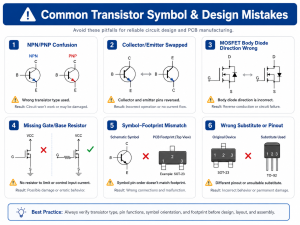
You may also like

Decoupling vs Bypass Capacitor: Differences and PCB Use

June 16th, 2026

Decoupling vs bypass capacitor is a common question in PCB design because the two terms are often used together. In many circuits, they may even refer to the same physical capacitor placed near an IC power pin.

The simple answer is this: a decoupling capacitor helps reduce the effect of power supply disturbances between circuit blocks, while a bypass capacitor gives high-frequency noise a low-impedance path to ground.

In practical PCB design, one capacitor can often perform both functions. For example, a 100 nF ceramic capacitor placed close to an IC power pin can help stabilize the local power supply and bypass high-frequency noise to ground.

The key difference is not only the capacitor itself. It is more about why the capacitor is used, where it is placed, and what type of noise or power disturbance it needs to control.

Decoupling vs Bypass Capacitor

What Is a Decoupling Capacitor?

A decoupling capacitor is used to reduce the interaction between different parts of a circuit through the power supply. It helps one circuit block avoid being affected by voltage noise or current changes from another circuit block.

When an IC switches, it may draw current very quickly. This sudden current demand can cause voltage dips or noise on the power rail. A decoupling capacitor provides local charge near the IC, so the power supply voltage stays more stable.

In PCB design, a decoupling capacitor is usually placed between the power pin and ground pin of an IC.

Its main purposes are:

  • Stabilize the power supply near the IC
  • Reduce voltage dips during switching
  • Provide local energy storage
  • Reduce noise coupling between circuit blocks
  • Improve digital and mixed-signal circuit reliability

For example, microcontrollers, FPGAs, memory chips, high-speed logic ICs, and mixed-signal devices usually need decoupling capacitors close to their power pins. Without proper decoupling, the circuit may have unstable operation, signal noise, reset problems, or EMI issues.

Decoupling vs Bypass Capacitor

What Is a Bypass Capacitor?

A bypass capacitor is used to send unwanted AC noise to ground. It provides a low-impedance path for high-frequency noise, so the noise does not continue through the power rail or enter sensitive parts of the circuit.

In many PCB circuits, a bypass capacitor is also placed between VCC and ground. For DC voltage, the capacitor blocks current after it is charged. For high-frequency noise, the capacitor behaves like a low-impedance path and allows the noise to return to ground.

Its main purposes are:

  • Bypass high-frequency noise to ground
  • Reduce ripple on the power rail
  • Keep unwanted AC noise away from sensitive circuits
  • Improve power integrity
  • Reduce high-frequency interference

A bypass capacitor is commonly used near ICs, analog circuits, amplifiers, sensors, power supply inputs, and other noise-sensitive areas.

The word “bypass” emphasizes the noise path. The capacitor allows unwanted high-frequency noise to bypass the active circuit and return to ground.

Decoupling vs Bypass Capacitor

Decoupling vs Bypass Capacitor: Are They the Same?

Decoupling capacitors and bypass capacitors are closely related, but they are not always exactly the same.

In many PCB designs, the same capacitor can be called both a decoupling capacitor and a bypass capacitor. For example, a 100 nF ceramic capacitor near an IC power pin can decouple the IC from power rail disturbance and also bypass high-frequency noise to ground.

However, the two terms focus on different functions:

TermMain FocusTypical Meaning
Decoupling capacitorIsolation between circuit blocksReduces power rail disturbance and local voltage fluctuation
Bypass capacitorNoise path to groundProvides a low-impedance path for high-frequency noise
In PCB practiceOften the same componentA capacitor near an IC power pin may perform both functions

A simple way to understand the difference is:

  • Decoupling focuses on keeping the local power supply stable.
  • Bypassing focuses on sending unwanted high-frequency noise to ground.

This is why engineers often use the two terms together. The physical capacitor may be the same, but the explanation depends on which problem it is solving.

What Is the Main Difference Between Decoupling and Bypass Capacitors?

The main difference between a decoupling capacitor and a bypass capacitor is the design purpose.

A decoupling capacitor is mainly used to maintain a stable local supply voltage. It provides short bursts of charge when the IC suddenly needs current. This helps reduce voltage drops and prevents one circuit block from disturbing another through the power rail.

A bypass capacitor is mainly used to reduce high-frequency noise. It gives AC noise a short path to ground, so the noise does not travel through the circuit.

The difference can be explained like this:

  • Decoupling capacitor: “Keep the IC power supply stable.”
  • Bypass capacitor: “Send unwanted high-frequency noise to ground.”

In real PCB design, these two functions often happen at the same time. A capacitor close to the IC power pin can supply local current and reduce high-frequency noise. That is why the two terms are often mixed.

For design work, the more important questions are:

  • Is the capacitor close enough to the IC power pin?
  • Is the ground connection short and low impedance?
  • Is the capacitor value suitable for the noise frequency?
  • Is the package suitable for high-frequency performance?
  • Is the power and ground plane structure designed properly?

In many cases, good PCB layout matters more than the name used for the capacitor.

How Do Decoupling and Bypass Capacitors Work in a Circuit?

Decoupling and bypass capacitors work because a capacitor behaves differently with DC voltage and AC noise.

For DC power, the capacitor charges and acts like a small local energy reservoir. When the IC suddenly switches and needs current, the capacitor can provide charge quickly. This helps reduce voltage droop at the IC power pin.

For high-frequency noise, the capacitor provides a low-impedance path to ground. This helps keep noise away from the power rail and sensitive signal paths.

A simple process looks like this:

  • The IC switches and creates a fast current demand.
  • The local capacitor supplies part of this current.
  • The voltage change on the power rail is reduced.
  • High-frequency noise flows through the capacitor to ground.
  • The circuit becomes more stable and less noisy.

The capacitor does not work alone. Its actual performance also depends on:

  • Capacitance value
  • Capacitor package
  • Equivalent series resistance, or ESR
  • Equivalent series inductance, or ESL
  • Distance from the IC power pin
  • Via placement
  • Power and ground plane design
  • PCB stack-up

For high-frequency circuits, physical layout is very important. Even if the capacitor value is correct, the capacitor may not work well if it is placed too far away from the IC.

Where Should Decoupling and Bypass Capacitors Be Placed on a PCB?

Decoupling and bypass capacitors should be placed as close as practical to the IC power pin and ground return path. The goal is to keep the current loop short and low impedance.

Good placement rules include:

  • Place the capacitor close to the IC power pin.
  • Connect the capacitor to ground with a short path.
  • Keep traces short and wide where possible.
  • Avoid long, thin traces between the capacitor and IC.
  • Use nearby vias to connect to power and ground planes.
  • Place high-frequency, small-value capacitors closest to the IC.
  • Place larger-value bulk capacitors near the power rail, regulator output, or power input.

For a typical IC, a common practice is to place a small-value ceramic capacitor, such as 100 nF, near each power pin or power pin group. Here, “small-value” refers mainly to capacitance value, not only physical size.

Larger-value capacitors, such as 1 µF, 4.7 µF, 10 µF, or higher, may be placed near the power rail, regulator output, power input, or a group of ICs. These capacitors help support lower-frequency voltage changes and provide more local energy storage.

Poor placement can reduce capacitor effectiveness. A decoupling capacitor placed far from the IC may still appear in the schematic, but it may not help much at high frequency because the trace inductance is too high.

For PCB layout, the practical rule is simple: the capacitor should be close to the noise source and close to the ground return path.

What Capacitor Values Are Commonly Used?

Common capacitor values depend on the circuit speed, power rail, IC type, noise frequency, and PCB layout. There is no single value that works for every design.

However, some values are widely used in PCB design:

Common ValueAlso Written AsTypical Use
10 nF0.01 µFHigher-frequency bypassing
100 nF0.1 µFCommon IC decoupling capacitor
1 µF1,000 nFLocal power rail support
4.7 µF4,700 nFBulk decoupling near IC groups
10 µF10,000 nFPower input or rail stabilization
47 µF or higher47,000 nF or higherBulk energy storage and low-frequency filtering

A common design approach is:

  • Use a 100 nF ceramic capacitor near the IC power pin for local high-frequency decoupling.
  • Add 1 µF to 10 µF capacitors near power rails, regulator outputs, or IC groups for local energy support.
  • Use 47 µF or larger bulk capacitors near power inputs or regulator outputs for lower-frequency filtering and energy storage.

In this context, “small capacitor” and “large capacitor” usually refer to capacitance value. A 100 nF capacitor is a small-value capacitor. A 10 µF or 47 µF capacitor is a larger-value capacitor.

Capacitance and physical size are related, but they are not exactly the same. In the same capacitor type, voltage rating, dielectric material, and product series, a larger capacitance value often requires a larger package. However, physical size also depends on capacitor type, voltage rating, dielectric, temperature performance, DC bias behavior, and manufacturer design.

For example, a 10 µF ceramic capacitor may be available in a small SMD package, but its effective capacitance can drop under DC bias. A larger package or different capacitor type may be needed if stable capacitance is important.

How to Choose the Right Decoupling or Bypass Capacitor?

Choosing a decoupling or bypass capacitor requires more than selecting a common value. The right choice depends on the circuit, frequency, power rail, capacitor type, and PCB layout.

Check these points first:

  • Circuit function
    Digital ICs, analog circuits, RF circuit boards, and power circuits may need different capacitor values and placement methods.
  • Capacitance value
    100 nF is common for local IC decoupling, but larger or smaller values may be needed depending on the frequency range.
  • Capacitor type
    MLCC ceramic capacitors are widely used for high-frequency decoupling. Tantalum, aluminum electrolytic, and polymer capacitors may be used for larger capacitance or bulk support.
  • Dielectric type
    X7R and X5R MLCCs are common for decoupling. C0G/NP0 capacitors are more stable, but they usually have smaller capacitance values.
  • Voltage rating
    Choose a voltage rating higher than the working voltage. Avoid using capacitors too close to their rated voltage limit.
  • DC bias behavior
    MLCC capacitance can drop when DC voltage is applied. This is important for power rail decoupling.
  • Package size
    Smaller packages often have lower ESL and better high-frequency performance, but they may have lower effective capacitance.
  • Placement
    A well-placed capacitor often performs better than a theoretically correct capacitor placed far away.
  • Ground connection
    Use a short, direct ground return path. Poor grounding can reduce bypass performance.

For many digital PCB designs, a practical starting point is to place a 100 nF ceramic capacitor close to each IC power pin or power pin group. This small-value capacitor helps reduce high-frequency noise near the IC.

Larger-value capacitors, such as 1 µF, 4.7 µF, or 10 µF, may be added near the power rail, regulator output, or IC groups to support lower-frequency voltage changes and provide more local energy storage.

For critical high-speed, RF, automotive, medical, or industrial products, capacitor selection should be checked against the IC datasheet, power integrity requirements, PCB stack-up, and layout review.

Common PCB Layout Mistakes with Decoupling and Bypass Capacitors

Many decoupling problems are not caused by the capacitor value. They are caused by PCB layout.

Common mistakes include:

  • Placing the capacitor too far from the IC
    Long traces add inductance and reduce high-frequency performance.
  • Using a long ground return path
    A poor ground path increases loop area and noise.
  • Using long, thin traces unnecessarily
    Long and narrow traces increase impedance.
  • Putting vias in the wrong location
    Via placement affects the current loop. Ground vias should be close and direct.
  • Using only one bulk capacitor for many ICs
    A bulk capacitor alone cannot handle local high-frequency switching noise at each IC.
  • Ignoring capacitor package parasitics
    Larger physical capacitors may not work well at high frequency because of higher ESL.
  • Confusing capacitance value with physical size
    A larger capacitance value does not automatically mean better high-frequency performance. Package size, ESL, ESR, and placement also matter.
  • Copying the schematic without layout review
    A correct schematic does not guarantee good power integrity.
  • Not checking the IC datasheet
    Some ICs require specific decoupling values and placement instructions.

A better layout approach is:

  • Place small-value ceramic capacitors closest to the IC power pins.
  • Keep the loop between the power pin, capacitor, and ground as short as possible.
  • Use a solid ground plane when possible.
  • Add larger-value bulk capacitors near regulators or power entry points.
  • Review decoupling placement during DFM and layout checking.

For PCB assembly, capacitor polarity, package, footprint, and placement should also be checked before production. A wrong footprint or wrong capacitor orientation can cause assembly defects or circuit failure.

FAQs About Decoupling vs Bypass Capacitor

What Is the Difference Between a Decoupling Capacitor and a Bypass Capacitor?

A decoupling capacitor helps isolate circuit blocks from power supply disturbances. A bypass capacitor provides a low-impedance path for high-frequency noise to ground. In many PCB designs, the same capacitor can perform both functions.

Are Decoupling and Bypass Capacitors the Same?

They are often the same physical capacitor, especially when placed near an IC power pin. The difference is mainly in the function being described. Decoupling focuses on supply stability, while bypassing focuses on noise removal.

Why Is a 100 nF Capacitor Commonly Used?

A 100 nF capacitor, also written as 0.1 µF, is commonly used because it works well for local IC decoupling in many digital circuits. It is small in capacitance value, widely available, and effective for reducing high-frequency noise when placed close to the IC.

Does “Small Capacitor” Mean Small Size or Small Capacitance?

In decoupling discussions, “small capacitor” usually means small capacitance value, such as 10 nF or 100 nF. The physical size may also be small, but size depends on package, voltage rating, dielectric type, and manufacturer design.

Are Larger-Value Capacitors Always Physically Larger?

Not always. In the same capacitor type and voltage rating, larger capacitance often needs a larger package. However, physical size also depends on dielectric material, capacitor structure, voltage rating, temperature performance, and DC bias behavior.

Where Should a Bypass Capacitor Be Placed?

A bypass capacitor should be placed close to the IC power pin and connected to ground through a short, low-impedance path. Poor placement can reduce its high-frequency performance.

Where Should a Decoupling Capacitor Be Placed?

A decoupling capacitor should be placed near the power pin of the IC or circuit block it supports. The goal is to provide local charge and reduce power rail disturbance.

Can I Use One Capacitor for Both Decoupling and Bypassing?

Yes. In many PCB designs, one capacitor can serve both purposes. A ceramic capacitor close to an IC power pin can stabilize the local supply and bypass high-frequency noise to ground.

What Value Should I Use for a Decoupling Capacitor?

A common starting value is 100 nF for local IC decoupling. Larger values such as 1 µF, 4.7 µF, or 10 µF may be added for lower-frequency support or bulk decoupling.

Is a Larger Capacitance Value Always Better?

No. Larger capacitance does not always mean better high-frequency performance. Package size, ESL, ESR, placement, and frequency behavior also matter.

Do All ICs Need Decoupling Capacitors?

Most digital ICs and many analog ICs need decoupling capacitors. The exact value and placement should follow the IC datasheet and PCB layout requirements.

What Happens If I Do Not Use Decoupling Capacitors?

The circuit may suffer from voltage dips, noise, unstable logic operation, EMI problems, false triggering, reset issues, or poor signal integrity.

In a nutshell, decoupling vs bypass capacitor is mainly a difference in function. A decoupling capacitor helps stabilize the local power supply, while a bypass capacitor provides a low-impedance path for high-frequency noise to ground.

In practical PCB design, the same SMD ceramic capacitor often performs both jobs, especially when placed close to an IC power pin. For many digital circuits, a 100 nF ceramic capacitor is a common starting point for local high-frequency decoupling, while larger-value capacitors may be added near power rails or regulator outputs for extra energy support.

The key is not only choosing the right capacitance value. Placement, package size, ground path, power plane design, and circuit frequency all affect capacitor performance. For high-speed, RF, industrial, medical, or automotive electronics, capacitor selection and PCB layout should be reviewed carefully before production.

Need medical PCB assembly services, BOM review, capacitor selection, or DFM checking? Pls feel free to send your Gerber files, BOM, stack-up, and project requirements to EBest Circuit (Best Technology) at sales@bestpcbs.com.
You may also like

SMD Capacitor: Sizes, Codes, Polarity and Selection

June 16th, 2026

An SMD capacitor is a surface-mount capacitor soldered directly onto PCB pads. It is widely used in modern PCB assembly because it saves space, supports automated SMT production, and works well in compact electronic circuits.

However, choosing or replacing an SMD capacitor is not always as simple as matching one number. You may need to check its capacitance value, package size, voltage rating, dielectric type, polarity, footprint, and circuit function. Many small ceramic SMD capacitors also have no printed marking, which makes identification more difficult.

This guide explains SMD capacitor values, codes, sizes, polarity, types, selection rules, and testing methods in a practical way.

SMD Capacitor

What Is an SMD Capacitor?

An SMD capacitor is a capacitor designed for surface mount technology. Instead of using long leads that pass through PCB holes, it is mounted directly on solder pads on the PCB surface.

A typical SMD capacitor has:

  • A compact body
  • Metal terminations or leads
  • A capacitance value
  • A voltage rating
  • A dielectric material
  • A package size
  • A tolerance and temperature rating

The most common SMD capacitor is the MLCC, or multilayer ceramic capacitor. MLCCs are widely used because they are small, low-cost, non-polarized, and suitable for automated SMT assembly.

SMD capacitors are commonly used for:

  • Decoupling
  • Bypassing
  • Filtering
  • Coupling
  • Timing
  • Noise suppression
  • Power rail stabilization
  • RF tuning
  • Signal conditioning

In simple terms, an SMD capacitor stores and releases electrical charge in a compact package. It helps circuits operate more stably while reducing PCB space.

What Does SMD Mean on a Capacitor?

SMD means Surface Mount Device. On a capacitor, it means the component is made for surface mounting on a PCB.

SMD does not define the capacitance value, voltage rating, dielectric material, or polarity. It only describes the mounting style.

An SMD capacitor can be:

  • Ceramic
  • Tantalum
  • Aluminum electrolytic
  • Polymer
  • Film
  • Specialty capacitor

For example, a 100 nF ceramic capacitor in a 0603 package and a 100 µF SMD electrolytic capacitor are both SMD capacitors. But they are used in different circuits and follow different selection rules.

So when you see “SMD capacitor,” the next questions should be:

  • What is the capacitance value?
  • What is the package size?
  • What is the voltage rating?
  • Is it polarized?
  • What dielectric or capacitor type is used?
  • What is its function in the circuit?

What Is the Value of an SMD Capacitor?

The value of an SMD capacitor is its capacitance. It tells how much electrical charge the capacitor can store. Capacitance is usually measured in pF, nF, or µF.

Different units are used because capacitor values cover a wide range:

  • Small capacitance values are usually written in pF
  • Medium capacitance values are often written in nF
  • Larger capacitance values are usually written in µF

A simple way to understand the units is:

Value RangeCommon UnitTypical Example
Small capacitancepF10 pF, 100 pF
Medium capacitancenF1 nF, 10 nF, 100 nF
Large capacitanceµF1 µF, 10 µF, 47 µF

Common SMD capacitor values include:

Common ValueAlso Written AsTypical Use
10 pF0.01 nFRF circuits and timing circuits
100 pF0.1 nFSignal filtering
1 nF1,000 pF / 0.001 µFNoise filtering
10 nF0.01 µFCoupling or filtering
100 nF0.1 µFIC decoupling
1 µF1,000 nFPower rail stabilization
10 µF10,000 nFPower rail support
47 µF or higher47,000 nF or higherPower input filtering and energy storage

A very common SMD capacitor value is 100 nF, also written as 0.1 µF. It is often placed near IC power pins to reduce voltage noise.

The correct value depends on the circuit function. A decoupling capacitor, RF capacitor, timing capacitor, coupling capacitor, and power input capacitor may all need different values, even if they look similar on the PCB.

How to Identify an SMD Capacitor on a PCB?

Identifying an SMD capacitor on a PCB depends on its size, package, marking, and location. Larger SMD capacitors may have printed markings, while small ceramic capacitors are often blank.

You can identify an SMD capacitor by checking:

  • PCB reference designator
    Capacitors are usually marked as C1, C2, C10, C101, or similar on the PCB silkscreen.
  • Component shape
    MLCCs are usually small rectangular blocks. Tantalum and electrolytic capacitors are often larger and may show polarity marks.
  • Color and body style
    Ceramic capacitors are often beige, brown, gray, or off-white. Tantalum capacitors may be yellow or black. Aluminum electrolytic capacitors are often cylindrical.
  • Marking or code
    Some larger SMD capacitors show capacitance, voltage, polarity, or manufacturer codes.
  • Circuit location
    A capacitor near an IC power pin is often used for decoupling. A capacitor near a power input may be used for filtering or bulk energy storage.
  • BOM and schematic
    The most reliable source is the BOM, schematic, assembly drawing, or original component part number.
  • Measurement
    An LCR meter can help measure capacitance, but in-circuit measurement may be affected by other components.

Do not rely only on color or size. Two MLCCs with the same package and color may have completely different values. For repair or replacement, confirm the value through design files, circuit function, markings, or measurement after removal.

How to Read SMD Capacitor Codes and Markings?

SMD capacitor codes depend on the capacitor type. Some SMD capacitors have printed codes, but many small MLCCs do not.

Most small ceramic SMD capacitors in 0201, 0402, 0603, and 0805 packages are unmarked. Their values are usually confirmed by the BOM, reel label, schematic, or measurement.

When a capacitor uses a three-digit code, the first two digits are the base number, and the third digit tells how many zeros are added in pF.

CodeValueAlso Written As
101100 pF0.1 nF
1021 nF1,000 pF
10310 nF0.01 µF
104100 nF0.1 µF
1051 µF1,000 nF
10610 µF10,000 nF

Example:

104 = 10 + 4 zeros = 100,000 pF = 100 nF = 0.1 µF

For tantalum and aluminum electrolytic SMD capacitors, markings may show:

  • Capacitance
  • Voltage rating
  • Polarity
  • Manufacturer code
  • Series code
  • Date or lot code

For example, a capacitor marked “10 16V” may indicate 10 µF and 16V, but marking rules vary by manufacturer. Always confirm with the datasheet when the marking is unclear.

What Are Common SMD Capacitor Sizes?

SMD capacitor size refers to the physical package dimensions of the component. The package size affects PCB space, capacitance range, voltage rating, assembly difficulty, inspection, rework, and reliability.

Common SMD capacitor sizes include 0201, 0402, 0603, 0805, 1206, 1210, 1812, and 2220.

Imperial
Code
Metric
Code
Approx.
Dimensions (mm)
Approx.
Dimensions (inch)
Common
Use
020106030.6 × 0.30.024 × 0.012Ultra-compact modules
040210051.0 × 0.50.040 × 0.020Mobile devices and compact PCBA
060316081.6 × 0.80.063 × 0.031General electronics
080520122.0 × 1.250.079 × 0.049Industrial boards and prototypes
120632163.2 × 1.60.126 × 0.063Power rails and larger capacitance
121032253.2 × 2.50.126 × 0.098Higher capacitance or voltage
181245324.5 × 3.20.177 × 0.126Higher voltage or power circuits
222057505.7 × 5.00.224 × 0.197High capacitance or special use

Small packages save space, but they can be harder to assemble, inspect, and rework. They may also have weaker real capacitance performance under DC bias.

Larger packages need more PCB area, but they may support higher capacitance, higher voltage, better solder joint visibility, and easier repair.

For example, a 10 µF ceramic capacitor in a very small package may lose a large part of its effective capacitance under DC bias. A larger package or higher voltage rating may perform better in real operation.

SMD Capacitor

SMD Capacitor Size Chart and Footprint Dimensions

An SMD capacitor package and an SMD capacitor footprint are related, but they are not the same.

  • Package size means the physical size of the capacitor body.
  • Footprint means the PCB solder pad pattern used to mount the capacitor.
  • Land pattern is another term for the PCB pad design.
  • Pad gap affects alignment and soldering result.
  • Pad size affects solder wetting, fillet shape, and inspection.

A good footprint should support:

  • Stable pick-and-place alignment
  • Proper solder joint formation
  • Enough solder wetting area
  • Reliable reflow soldering
  • Lower tombstoning risk
  • Manufacturable spacing from nearby parts
  • Easier inspection and rework when needed

Footprint problems can cause:

  • Tombstoning
  • Component skew
  • Open solder joints
  • Weak solder joints
  • Solder beading
  • Poor wetting
  • Difficult inspection

Do not copy a footprint randomly from another design. The correct land pattern may depend on the capacitor package, manufacturer recommendation, solder paste thickness, reflow process, PCB surface finish, assembly capability, and inspection requirement.

For reliable PCBA manufacturing, confirm both the SMD capacitor package and the recommended footprint before finalizing the PCB layout.

What Are the Main Types of SMD Capacitors?

SMD capacitors are available in several types. Each type has different electrical behavior, size, cost, polarity, voltage range, and application area.

The main types include:

  • SMD ceramic capacitor / MLCC
  • SMD tantalum capacitor
  • SMD aluminum electrolytic capacitor
  • SMD polymer capacitor
  • SMD film capacitor

SMD Ceramic Capacitor

SMD ceramic capacitors are the most common type. Most are MLCCs.

They are widely used because they are:

  • Small
  • Low-cost
  • Non-polarized
  • Good for high-frequency circuits
  • Suitable for automated SMT assembly
  • Available in many package sizes

Common applications include decoupling, bypassing, filtering, RF circuits, and general PCB design.

The key point to remember is DC bias. High-capacitance MLCCs may lose effective capacitance when voltage is applied, especially in small packages.

SMD Tantalum Capacitor

SMD tantalum capacitors are often used when higher capacitance density and stable capacitance are needed.

They are commonly used in:

  • Power rails
  • Filtering circuits
  • Compact power designs
  • Some industrial and communication electronics

They are polarized, so correct orientation is required. Reverse voltage or surge current may cause failure, so voltage derating is important.

SMD Aluminum Electrolytic Capacitor

SMD aluminum electrolytic capacitors are usually used for larger capacitance values.

They are common in:

  • Power input filtering
  • Bulk energy storage
  • Power supply circuits
  • Industrial electronics

They are polarized and usually larger than ceramic capacitors. ESR, ripple current, temperature, and lifetime should be checked before selection.

SMD Polymer Capacitor

SMD polymer capacitors are used when the circuit needs low ESR and better ripple current performance.

They are useful for:

  • DC-DC converters
  • Power rails
  • High-current power circuits
  • Low-ESR filtering

They usually cost more than standard electrolytic capacitors, but they can provide better power performance.

SMD Film Capacitor

SMD film capacitors are less common than MLCCs, but they are useful in circuits that need stability, low loss, or pulse performance.

They may be used in:

  • Signal circuits
  • Timing circuits
  • Pulse circuits
  • Selected power applications

They are often larger than ceramic capacitors, so they are not used everywhere.

SMD Capacitor

Are SMD Capacitors Polarized?

Some SMD capacitors are polarized, and some are non-polarized.

Most SMD ceramic capacitors are non-polarized. They can usually be installed in either direction because they do not have positive and negative terminals.

Common non-polarized types include:

  • MLCC ceramic capacitors
  • Some film capacitors
  • Some specialty capacitors

Tantalum, aluminum electrolytic, and many polymer capacitors are polarized. They must be installed in the correct direction.

Common polarized types include:

  • SMD tantalum capacitor
  • SMD aluminum electrolytic capacitor
  • SMD polymer capacitor

If a polarized capacitor is installed backwards, it may fail, heat up, leak, short, or damage the circuit.

You can check polarity by looking for:

  • Plus mark
  • Stripe mark
  • Beveled edge
  • Printed polarity symbol
  • PCB silkscreen
  • Datasheet orientation
  • Package style

Be careful because polarity markings differ by capacitor type. Tantalum capacitors often mark the positive side, while aluminum electrolytic capacitors often mark the negative side. If the marking is unclear, check the datasheet before assembly.

How to Choose SMD Capacitor Value, Voltage and Package?

Choosing the right SMD capacitor requires more than matching the capacitance value. A suitable capacitor should match the electrical requirement, package size, footprint, assembly process, and working environment.

Check these points before selection:

  • Capacitance value
    Select the required pF, nF, or µF value based on the circuit function.
  • Voltage rating
    Choose a voltage rating higher than the working voltage. Do not operate the capacitor too close to its rated limit.
  • Package size
    Match the package with PCB space, capacitance range, voltage rating, and assembly capability.
  • Dielectric type
    C0G/NP0, X7R, X5R, and other dielectrics behave differently. Use stable dielectrics for precision or temperature-sensitive circuits.
  • DC bias performance
    MLCC capacitance may drop under applied DC voltage. Check the datasheet curve when the capacitor is used on a DC power rail.
  • ESR and ripple current
    These are important for power supply, converter, and filtering applications.
  • Polarity
    Confirm whether the capacitor is polarized before assembly or replacement.
  • Footprint
    Make sure the package matches the PCB pad pattern.
  • Temperature range
    Match the capacitor to the product operating environment.
  • Availability
    For production, check supply stability and possible alternative parts.

Common mistakes include:

  • Choosing only by capacitance
  • Ignoring DC bias
  • Using too low a voltage rating
  • Confusing polarized and non-polarized capacitors
  • Using the wrong footprint
  • Replacing a capacitor only by size
  • Ignoring temperature and lifetime requirements

A better selection process is to check the BOM, schematic, datasheet, layout footprint, assembly process, and application conditions together.

For PCBA projects, BOM review before production can help confirm capacitor package, voltage rating, polarity, footprint, sourcing risk, and possible alternatives.

How to Test a Bad or Shorted SMD Capacitor?

Testing an SMD capacitor depends on whether it is still mounted on the PCB or removed from the circuit. In-circuit testing can be misleading because other components may be connected in parallel.

Common signs of a bad SMD capacitor include:

  • Short circuit
  • Burn marks
  • Cracking
  • Leakage
  • Bulging on electrolytic types
  • Low capacitance
  • High ESR
  • Power rail short
  • Circuit instability
  • Device not powering on

A practical testing process:

  • Start with visual inspection
    Check for cracks, burns, discoloration, leakage, lifted pads, or broken solder joints.
  • Check for short circuit
    Use a multimeter in resistance or continuity mode. A very low resistance reading may indicate a short, but in-circuit results can be affected by the rest of the circuit.
  • Measure capacitance
    Use a multimeter with capacitance mode or an LCR meter. For better accuracy, remove the capacitor or lift one side.
  • Check ESR if needed
    ESR is important for electrolytic, polymer, and power-related capacitors.
  • Isolate the suspected capacitor
    If many capacitors are connected to the same power rail, one shorted capacitor can make all of them appear shorted. Removing or isolating the suspected part gives a more reliable result.

For unknown parts, check the schematic, BOM, reference designator, or a known-good board before replacement.

SMD Capacitor vs Through-Hole Capacitor: What Is the Difference?

SMD capacitors and through-hole capacitors perform the same basic electrical function, but they differ in mounting method, size, assembly process, PCB density, and repairability.

ItemSMD CapacitorThrough-Hole Capacitor
MountingSoldered on PCB surfaceLeads pass through PCB holes
SizeSmallerLarger
PCB densityHigherLower
AssemblySMT reflow processWave, selective, or hand soldering
AutomationExcellentSlower for mass production
RepairHarder for tiny packagesEasier for manual repair
Mechanical strengthGood for small partsStronger for large components
Common useCompact electronics and mass production PCBAPower parts, prototypes, repairable boards

SMD capacitors are preferred in compact and high-volume electronics because they save space and support automated placement. Through-hole capacitors are still useful for large capacitance, stronger mechanical support, prototypes, repairable devices, and some power applications.

Many PCB assemblies use both. Small ceramic capacitors may be SMD, while larger electrolytic capacitors or mechanically stressed parts may use through-hole packages.

FAQs About SMD Capacitor

What Is an SMD Capacitor?

An SMD capacitor is a surface-mount capacitor soldered directly onto PCB pads. It is commonly used for decoupling, filtering, coupling, bypassing, and power stabilization.

What Does SMD Mean on a Capacitor?

SMD means Surface Mount Device. It describes the mounting style, not the capacitance value, voltage rating, or capacitor type.

Are All SMD Capacitors Ceramic?

No. Many SMD capacitors are ceramic MLCCs, but SMD capacitors can also be tantalum, aluminum electrolytic, polymer, film, or specialty capacitors.

Do SMD Capacitors Have Polarity?

Some do and some do not. Ceramic SMD capacitors are usually non-polarized. Tantalum, aluminum electrolytic, and many polymer SMD capacitors are polarized.

How Can I Identify an SMD Capacitor Value?

Check the BOM, schematic, reel label, datasheet, or component marking. For small MLCCs, there may be no printed marking, so measurement or design files may be needed.

What Is a 104 SMD Capacitor Value?

A 104 SMD capacitor is usually 100 nF, also written as 0.1 µF, if it uses the standard three-digit capacitor code.

What Is a 105 SMD Capacitor Value?

A 105 SMD capacitor is usually 1 µF, also written as 1,000 nF, under the standard three-digit capacitor code.

What Is a 106 SMD Capacitor Value?

A 106 SMD capacitor is usually 10 µF, also written as 10,000 nF, under the standard three-digit capacitor code.

What Are Common SMD Capacitor Sizes?

Common SMD capacitor sizes include 0201, 0402, 0603, 0805, 1206, 1210, 1812, and 2220.

What Is the Difference Between SMD Capacitor Package and Footprint?

The package is the physical size of the capacitor. The footprint is the PCB solder pad pattern used to mount it. Both must match for reliable soldering.

Can I Replace an SMD Capacitor With a Larger Package?

Sometimes, if the PCB footprint allows it and the electrical specifications match. However, the part must fit the pad layout and assembly process.

Can I Use a Higher Voltage SMD Capacitor?

Usually yes, if the capacitance, dielectric, package, footprint, and circuit requirement are suitable. A higher voltage rating can provide better margin, but size and cost may increase.

How Do I Know if an SMD Capacitor Is Bad?

Check for cracks, burns, leakage, shorts, low capacitance, high ESR, or circuit symptoms. An LCR meter gives better results than a basic multimeter.

Can a Shorted SMD Capacitor Be Tested In-Circuit?

It can be suspected in-circuit, but not always confirmed. Other components may be connected in parallel. Removing the capacitor or lifting one side gives a more reliable result.

Overall, SMD capacitor selection is not only about choosing a capacitance value. A reliable choice should consider package size, footprint, code, dielectric type, voltage rating, polarity, DC bias, ESR, temperature range, assembly process, and actual circuit function.

For simple circuits, a standard MLCC may be enough. For power rails, automotive electronics, industrial control PCBs, compact PCBA projects, or high-reliability products, the capacitor package and real operating conditions become more important.

If you need SMT board assembly, BOM review, SMD capacitor selection support, or DFM checking for your PCBA project, pls feel free to send your Gerber files, BOM, stack-up, and project requirements to EBest Circuit (Best Technology) at sales@bestpcbs.com.

You may also like