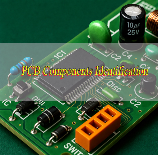
PCB components identification is the process of recognizing every electronic part mounted on a PCB by checking board markings, reference designators, PCB symbols, package shape, body codes, polarity marks, footprint and BOM data. It helps users understand what each component is, what it does and whether it matches the design.
For repair, inspection, reverse engineering, component sourcing and PCBA production, one visual clue is never enough. A reliable PCB components identification method combines PCB silkscreen, component markings, printed circuit board parts list, schematic, test tools and production inspection records. This guide explains how to identify PCB components clearly and practically.
What Is PCB Components Identification?
PCB components identification means matching each physical part on a PCB with its type, value, package, polarity, rating and circuit function. It helps users recognize resistors, capacitors, inductors, diodes, transistors, ICs, connectors, fuses, relays and switches.
The process usually starts from visible PCB markings. Then the component body code, reference designator, package shape, pin count, PCB symbol and surrounding circuit are checked. If design files are available, the BOM and schematic provide stronger confirmation.
In real PCB assembly, many SMD parts are too small to show full markings. Some ceramic capacitors have no printed code, and some ICs only show short top marks. Therefore, PCB components identification should combine visual checking, documentation and testing.
Why Is PCB Components Identification Important?
Accurate PCB components identification reduces repair errors, wrong sourcing, assembly defects and production delays. It is important for PCB repair, prototype debugging, incoming inspection, SMT assembly, quality control and mass production.
Main benefits include:
- Faster troubleshooting when a PCB fails during testing.
- Better replacement accuracy when damaged parts must be changed.
- Lower BOM mismatch risk before SMT production.
- Improved first article inspection before batch assembly.
- Stronger traceability for component batches and approved substitutes.
- Clearer communication between engineers, buyers and PCB suppliers.
For purchasing teams, correct PCB components identification also helps avoid wrong part numbers, unsuitable replacements and counterfeit risks. In dense PCBA projects, it supports smoother quotation, sourcing and production approval.
What Tools Are Needed for PCB Board Components Identification?
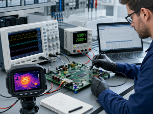
PCB board components identification requires visual tools, electrical tools, design documents and inspection equipment. A simple repair may only need a microscope and multimeter, while production-level PCB components identification often requires BOM review, AOI, X-ray and functional testing.
| Tool | Best Use | What to Check | Practical Note |
|---|---|---|---|
| Magnifier | Large parts and board text | Silkscreen, polarity, damage | Good for quick first inspection |
| Microscope | Small SMD parts | Top code, cracks, solder joints | Useful for 0201, 0402, QFN and fine-pitch ICs |
| Multimeter | Basic electrical checks | Resistance, continuity, diode direction | Check unpowered circuits first |
| LCR meter | Passive components | Capacitance, inductance, ESR | In-circuit readings may be affected |
| Bench power supply | Controlled power-up | Current draw, short protection | Set current limit before testing |
| Thermal camera | Fault location | Hot ICs, shorted rails, overload | Helpful for failed boards |
| Datasheet | Technical confirmation | Pinout, package, rating | Match top code and package together |
| BOM | Exact part verification | MPN, value, package, substitutes | Most important for PCBA sourcing |
| AOI | SMT inspection | Missing parts, wrong polarity, offset | Common in assembly production |
| X-ray | Hidden solder inspection | BGA, QFN, voids, bridges | Needed for hidden pads |
| ICT | Electrical production test | Nets, shorts, component presence | Useful for batch control |
| Functional tester | Final product behavior | Real operating performance | Confirms the board works as designed |
Before applying power, inspect the PCB for burned marks, shorted rails, reversed parts and damaged solder joints. For production projects, the best result comes from combining manual inspection, BOM checking and automated inspection instead of using only one tool.
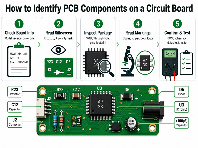
How to Identify PCB Components on a Circuit Board?
To identify PCB components on a circuit board, follow a fixed order from board information to final confirmation. This keeps PCB components identification clear, repeatable and safer than guessing from appearance only.
Step 1: Check the PCB model and revision.
Start with the board number, revision code, date code and assembly side. Board revision matters because the same reference designator may use different values or packages in different versions.
Step 2: Read the silkscreen and PCB symbols.
Look for R, C, L, D, Q, U, J, F, SW, TP and polarity signs. PCB symbols can show whether a part is related to resistance, capacitance, diode direction, IC pin 1, connector orientation or test access.
Step 3: Inspect package shape and footprint.
Check whether the part is SMD or through-hole. Then review body size, pad layout, pin pitch, number of terminals, thermal pad and mounting direction. A correct value with the wrong footprint may still fail assembly.
Step 4: Read the component marking.
Use a microscope to check SMD codes, logos, stripes, dots, notches, printed values and date codes. A short SMD code should not be used as final proof because it may not be unique.
Step 5: Confirm with documents and testing.
Compare the part with the BOM, schematic, datasheet and placement file. When needed, use a multimeter, LCR meter or diode mode to verify the component safely.
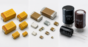
How to Read PCB Component Markings and Codes?
PCB component markings and codes are printed on the component body and should be read with package type, polarity, logo and circuit position. In PCB components identification, a short code alone is not enough for final confirmation.
| Part | Marking | Example |
|---|---|---|
| Resistor | 3-digit or 4-digit code | 103, 4701 |
| Capacitor | Value code or no marking | 104, 10µF |
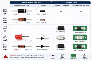
| Diode | Stripe, logo or code | Cathode band |
| Transistor | Short SMD code | SOT-23 code |
| IC | Top mark, logo, date code | Part code |
| Fuse | Current rating | 2A, F2A |
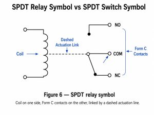
| Relay | Coil voltage and contact rating | 5V, 12V |
For PCB component identification code reading, the same short code may appear on parts from different manufacturers. Therefore, package size, pin count, logo, circuit function and datasheet matching should be checked together. This makes a PCB component markings guide more useful in repair, inspection and PCBA production.
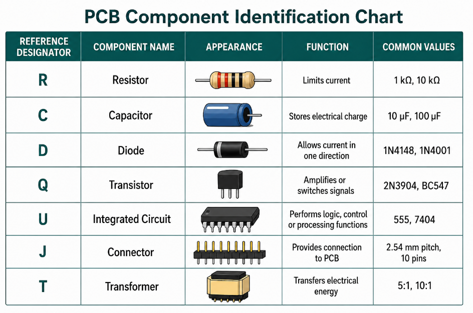
PCB Component Identification Chart
A PCB Component Identification Chart should help users check component type, board clue, body marking, package, polarity, rating and confirmation method in one place. It is not just a simple list of component names. It works as a practical PCB components identification guide before repair, sourcing or assembly.
| Component | Designator | Board Clue | Body Clue | Package Clue | Confirm By |
|---|---|---|---|---|---|
| Resistor | R | Near signal or divider circuit | Number code or color bands | 2 terminals, chip or axial | Resistance value, BOM |
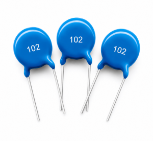
| Ceramic capacitor | C | Near IC power pins or filters | Often blank or small code | 2-terminal MLCC chip | Capacitance, BOM |
| Electrolytic capacitor | C | Power input or filtering area | Value, voltage, stripe | Cylindrical or can type | Polarity, capacitance |
| Inductor | L | Near DC-DC converter or filter | Code or blank body | Coil, ferrite or molded block | Inductance, current rating |
| Diode | D | Direction mark on silkscreen | Stripe or short code | 2-terminal SMD or axial | Diode mode, datasheet |
| Transistor | Q | Switching or control area | Short SMD code | 3-pin or power package | Pinout, datasheet |
| MOSFET | Q | Power switching area | Code and logo | SOT, TO, DFN or power package | Gate, drain, source check |
| IC | U / IC | Pin-1 mark or outline | Top mark, logo, date code | Multi-pin package | Datasheet, BOM |
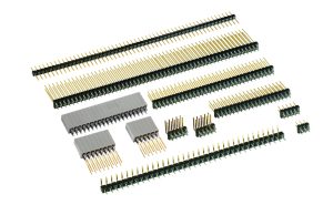
| Connector | J / P / CN | Pin number or outline | Usually no value code | Header, socket, terminal | Pin count, pitch, mating part |
| Fuse | F | Power input path | Current rating or code | SMD, cartridge, resettable | Continuity, current rating |
| Relay | K / RY / RL | Load switching area | Coil voltage, contact rating | Box package | Coil and contact datasheet |
| Switch | SW | User input area | Type or blank body | Tactile, slide, DIP | Footprint, operation test |
This chart is most useful when combined with the printed circuit board parts list, schematic, datasheet and test results. For field repair and supplier review, PCB components identification becomes more accurate when the chart is used as a checklist instead of a guess sheet. For unknown parts, use it to narrow the component group first, then confirm value, rating and package through documents or measurement.
How to Identify Passive Components on a PCB?
Passive components include resistors, capacitors and inductors. They do not amplify signals, but they strongly affect current, voltage, filtering, timing and power stability.
Step 1: Start with the reference designator.
R usually means resistor, C means capacitor, and L means inductor. This quickly separates passive parts from semiconductors, connectors and ICs during PCB components identification.
Step 2: Check the package and appearance.
Resistors and ceramic capacitors may both look like small rectangular chips, so do not judge by shape alone. Inductors are often larger, darker, magnetic or coil-shaped, especially in power circuits.
Step 3: Read the value mark if available.
Resistors may show 103, 472 or 1001. Ceramic capacitors may have no marking. Electrolytic capacitors usually show capacitance and voltage. Inductors may show a value code, but many power inductors are unmarked.
Step 4: Confirm rating and circuit role.
Use the BOM, LCR meter or datasheet to check resistance, capacitance, inductance, voltage rating, current rating, tolerance and temperature range. A correct value with the wrong voltage or current rating can still cause failure. This keeps PCB components identification focused on real electrical performance, not only visual appearance.
How to Identify Semiconductor Components on a PCB?
Semiconductor components include diodes, LEDs, transistors, MOSFETs, regulators, TVS diodes and ESD protection devices. They must be checked carefully because polarity, pinout and rating directly affect circuit safety.
Step 1: Check the designator.
D usually means diode, LED or TVS diode. Q usually means transistor or MOSFET. Some regulators may use U because they are IC-style devices.
Step 2: Read polarity and body marks.
A diode often has a cathode stripe. LEDs may have a flat edge, dot or pad mark. Transistors and MOSFETs often use short SMD codes, so the code must be checked with package and circuit location.
Step 3: Use circuit position to narrow the function.
A SOT-23 part near a connector may be ESD protection. A similar SOT-23 part near a power circuit may be a regulator, transistor or MOSFET driver. Position gives important context in PCB components identification.
Step 4: Confirm by datasheet or test.
Use diode mode, continuity checks and datasheet comparison before replacement. For power semiconductors, also confirm voltage rating, current rating, package heat dissipation and pinout.
How to Identify ICs and Microcontrollers on a PCB?
ICs and microcontrollers are identified by reference designator, top marking, logo, package type, pin count, pin-1 mark and surrounding circuit. They usually use U or IC designators.
Step 1: Read the top marking under magnification.
Check the printed code, manufacturer logo and date code. Some ICs show a full part number, while others only show a shortened top mark.
Step 2: Confirm the package type.
Check whether the IC is SOIC, QFN, QFP, BGA, LGA, DIP or another package. Package size, pitch and pin count can quickly narrow the possible device family.
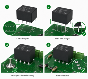
Step 3: Find pin 1 before any replacement.
Look for a dot, notch, bevel, chamfer or PCB pin-1 mark. Wrong orientation can damage the IC, short power rails or stop the board from booting.
Step 4: Study the surrounding circuit.
Microcontrollers are often connected to crystals, reset circuits, programming headers, decoupling capacitors and communication lines. Power ICs are often near inductors, diodes, MOSFETs and large capacitors.
Step 5: Confirm with BOM and datasheet.
Do not source or replace an IC from the top mark alone. Always confirm package, pinout, voltage, memory size, temperature grade and firmware requirements when applicable. In IC sourcing, PCB components identification should also consider firmware, programming status and lifecycle risk.
How to Identify Connectors, Fuses, Relays and Switches on a PCB?
Connectors, fuses, relays and switches are usually recognizable by shape, but rating, pinout and mechanical fit still need confirmation. These parts connect the PCB to power, signals, users or external equipment.
Step 1: Check the designator.
Connectors may use J, P or CN. Fuses use F. Relays may use K, RY or RL. Switches usually use SW.
Step 2: Identify the mechanical structure.
For connectors, check pin count, pitch, latch direction, mounting angle, height and mating style. For switches, check whether the part is tactile, slide, DIP, pushbutton or rotary.
Step 3: Confirm electrical rating.
Fuses require current and voltage rating. Relays require coil voltage and contact rating. Connectors require current capacity, insulation distance and mating reliability.
Step 4: Match the footprint and assembly height.
Do not replace these parts by appearance only. Pin layout, body size, housing direction, mechanical strength and height must match the PCB and enclosure design. For PCB components identification in sourcing work, mechanical fit and electrical rating must be checked together.
How to Identify PCB Component Polarity and Pin Orientation?
PCB component polarity and pin orientation must be checked before repair, replacement or assembly because reverse mounting can damage the circuit. This is critical for diodes, LEDs, electrolytic capacitors, tantalum capacitors, ICs, connectors and modules.
Step 1: Check the component body mark.
Look for a diode stripe, LED flat edge, capacitor stripe, IC dot, notch, bevel or connector key. These marks usually show direction or pin 1.
Step 2: Compare with PCB silkscreen.
The PCB may show +, -, pin 1, a shaded pad, diode symbol or connector outline. The board marking should match the component direction.
Step 3: Confirm with datasheet.
Some polarity marks are manufacturer-specific. Electrolytic capacitors often mark the negative side, while many tantalum capacitors mark the positive side.
Step 4: Stop if marks conflict.
If the body mark, PCB symbol and datasheet do not match, do not power the PCB. Check the BOM, schematic and assembly drawing first. Correct polarity checking is a key part of reliable PCB components identification.
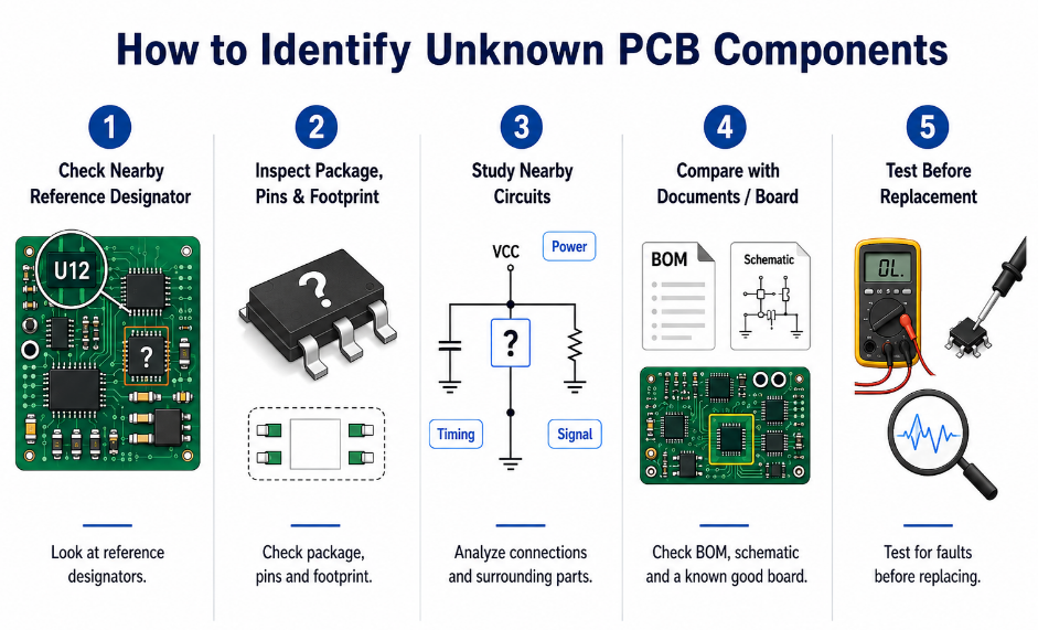
How to Identify Unknown or Unmarked PCB Components?
Unknown or unmarked PCB components should be identified by reference designator, package, footprint, circuit location, measurement, BOM comparison and similar board analysis. Guessing from shape alone can lead to wrong repair or sourcing.
Step 1: Check the nearby reference designator.
The designator gives the first clue. R, C, L, D, Q, U, F, J and SW point to different component groups.
Step 2: Inspect package, pins and footprint.
Package size, terminal count, thermal pad, pad layout and orientation marks can narrow the component type. A two-terminal part may be a resistor, capacitor, diode, fuse or inductor, so the circuit position matters.
Step 3: Study nearby circuits.
A part near power input may be protection, filtering or regulation. A part near a crystal may support timing. A part near a connector may be ESD protection or signal conditioning.
Step 4: Compare with documents or a known board.
Use the BOM, schematic, placement file or a working sample to confirm the part. If the board is damaged, compare the failed area with an undamaged board revision.
Step 5: Test before replacement.
For burned parts, check the root cause first. The damaged component may be the result of a short, overload or reverse polarity, not the original failure source. In difficult cases, PCB components identification should be reviewed before any replacement decision.
What Common Mistakes Happen During PCB Components Identification?
The most common mistakes during PCB components identification come from relying on one clue, ignoring ratings or skipping document checks. Each mistake can lead to wrong repair, wrong sourcing or failed PCBA assembly.
- Mistake: Treating reference designators as values.
Solution: Use R1, C2 or U3 only as location labels. Confirm value and part number through BOM, schematic or measurement. - Mistake: Trusting one SMD code as final proof.
Solution: Check package size, pin count, logo, circuit position and datasheet because short codes are not globally unique. - Mistake: Ignoring polarity and pin orientation.
Solution: Compare body marks, PCB silkscreen and datasheet before assembly or replacement. - Mistake: Replacing a burned part directly.
Solution: Check power rails, nearby loads, shorts and root cause before installing a new component. - Mistake: Matching components by appearance only.
Solution: Confirm voltage, current, tolerance, package, footprint, height and lifecycle status. - Mistake: Using substitutes without approval.
Solution: Review approved vendor list, BOM notes and customer requirements before changing any component.
FAQs About PCB Components Identification
Q1: What is the difference between PCB silkscreen and solder mask?
A1: PCB silkscreen is the printed text or symbol layer that shows reference designators, polarity marks, logos and assembly notes. Solder mask is the colored protective coating over copper. Silkscreen helps identification, while solder mask protects copper and defines exposed soldering areas. They work together but serve different purposes.
Q2: Can component values be measured directly on the PCB?
A2: Sometimes yes, but in-circuit measurement may be affected by parallel paths, connected IC pins or surrounding components. A resistor, capacitor or inductor may read differently while still mounted. For critical checking, compare with the BOM or lift one terminal carefully before measurement if the board design allows it.
Q3: What does DNP, DNI or NC mean in a BOM?
A3: DNP means do not populate, DNI means do not install, and NC usually means no connect or not connected depending on the context. These notes tell the assembly factory whether a component position should remain empty. Always check the BOM notes before assuming a missing component is an assembly defect.
Q4: Why does a replacement component fit but still fail?
A4: A component may fit the footprint but still have the wrong voltage rating, current rating, tolerance, temperature range, polarity, pinout or internal structure. Mechanical fit does not guarantee electrical compatibility. Before replacement, check the full datasheet and BOM requirement instead of relying only on package size. This is a common PCB components identification issue in repair and sourcing work.
Q5: How do test points help PCB troubleshooting?
A5: Test points give access to important nets such as power rails, ground, reset, communication lines or programming signals. They help technicians check voltage, continuity and signal behavior without touching tiny component pins. In production, test points also support ICT, functional testing and faster fault isolation.
Q6: Can conformal coating affect PCB component identification?
A6: Yes. Conformal coating can cover component markings, polarity signs, small SMD codes and solder joints. Microscope inspection, UV light or controlled coating removal may be required. Coating removal should be done carefully because aggressive scraping can damage pads, solder joints or component bodies.
Q7: How do counterfeit components affect PCBA reliability?
A7: Counterfeit components may have fake markings, poor internal structure, wrong die, weak plating or unstable electrical performance. They can pass visual inspection but fail during temperature, load or long-term operation. Reliable sourcing, approved suppliers and traceable purchasing records are important for PCBA reliability.
Q8: What files should I prepare before asking for PCBA quotation?
A8: Prepare Gerber files, BOM, CPL or placement file, schematic if available, assembly drawings, testing requirements and clear notes for special parts. Complete files help the factory check component availability, package match, polarity, substitutes and production risks. This also makes quotation faster and more accurate.
Q9: Why is board revision important for component checking?
A9: Different PCB revisions may use different component values, packages, footprints or approved substitutes. The same reference designator may not have the same value across different revisions. Always check the PCB revision before comparing BOM data, repairing a board or approving PCBA production.
Q10: How can buyers reduce BOM sourcing risk?
A10: Buyers can reduce risk by confirming manufacturer part numbers, lifecycle status, approved alternatives, minimum order quantity, lead time and material traceability. For mass PCBA projects, BOM review should happen before production starts. This helps avoid obsolete parts, wrong substitutes and urgent sourcing changes.
Q11: What should be checked when a component is missing from a PCB?
A11: First check whether the BOM marks that position as DNP, DNI or optional. Then confirm the board revision, placement file and assembly drawing. A missing part is not always a defect. Some positions are intentionally left empty for configuration, testing, cost control or different product versions.
Q12: How can a factory prevent wrong component loading during SMT assembly?
A12: A factory can reduce wrong loading by reviewing the BOM, verifying reels, checking feeder setup, using barcode control and performing first article inspection. AOI and functional testing provide additional protection after placement and soldering. Good material traceability also helps locate problems quickly if a batch issue appears.
PCB components identification is not just a repair skill. It is a practical quality-control method that connects PCB symbols, board markings, component codes, package shape, footprint, polarity, BOM data, testing and production records. The key technical point is clear: confirm every important component through multiple clues before repair, sourcing or assembly.
For PCBA projects, correct PCB components identification helps prevent wrong parts, wrong polarity, wrong substitutes and delayed production. EBest Circuit supports PCB fabrication, PCBA assembly, BOM review, component sourcing, SMT assembly, AOI, X-ray, ICT, functional testing and global delivery from our China source factory. Send your Gerber files, BOM and PCBA requirements to sales@bestpcbs.com for a fast quotation and reliable component sourcing support.