A transistor is one of the most important components in modern electronics. It can switch current, amplify signals, regulate power, drive loads, and form the basic building block of digital circuits. From small sensor modules to industrial control boards, power supplies, audio circuits, LED drivers, communication devices, and embedded systems, transistors appear almost everywhere.
This guide explains the transistor symbol, transistor symbol in PCB documentation, transistor symbol pinout, arrow meaning, NPN and PNP types, MOSFET and BJT symbols, switching use, voltage requirements, testing methods, common applications, and failure behavior.
What Is the Symbol for a Transistor?
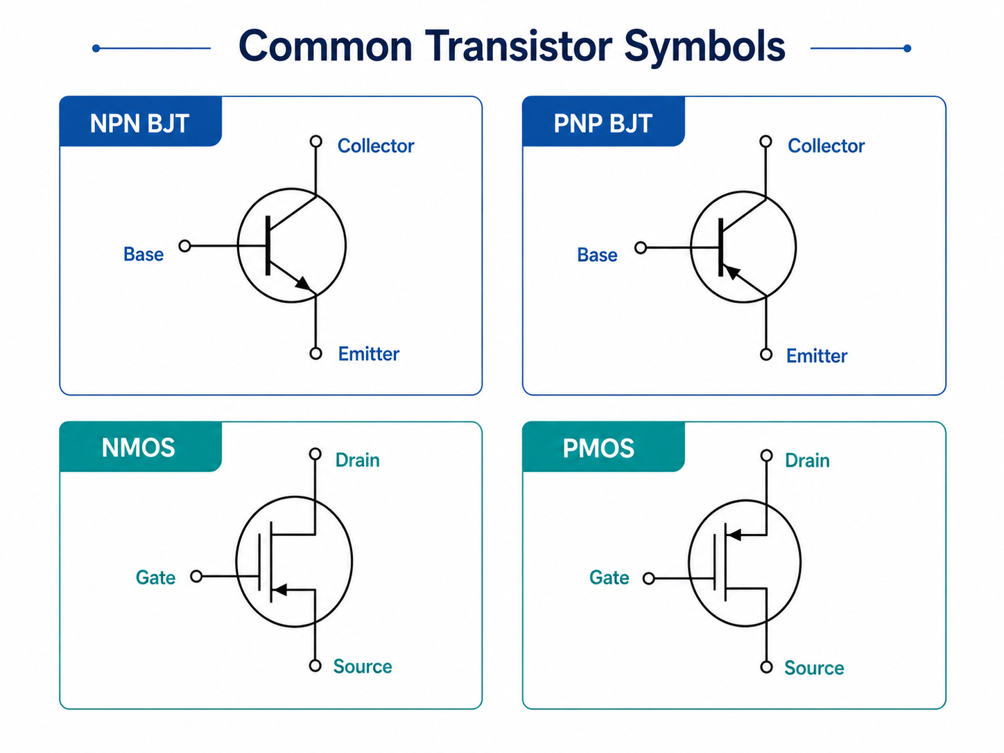
A transistor symbol is the schematic representation of a transistor in an electronic circuit diagram. It helps engineers understand how the transistor is connected and how current flows through the circuit.
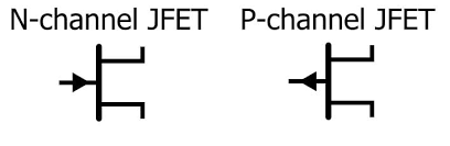
The most common transistor symbols are used for BJT transistors and MOSFET transistors.
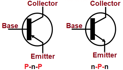
A BJT transistor symbol usually has three terminals:
| Terminal | Full Name | Main Function |
|---|---|---|
| B | Base | Controls the transistor |
| C | Collector | Receives or supplies main current |
| E | Emitter | Current output or reference terminal |
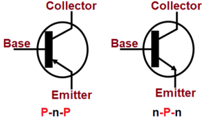
In an NPN or PNP BJT symbol, the arrow is placed on the emitter. The arrow direction helps identify whether the transistor is NPN or PNP.
A MOSFET transistor symbol also has three main terminals:
| Terminal | Full Name | Main Function |
|---|---|---|
| G | Gate | Controls conduction by voltage |
| D | Drain | Main current terminal |
| S | Source | Main current terminal or reference |
Some MOSFET symbols also show the body diode, substrate, or enhancement/depletion mode structure.
In simple terms, a transistor symbol tells you three things: what type of transistor it is, where each pin connects, and how the device controls current.
Transistor Symbol in PCB
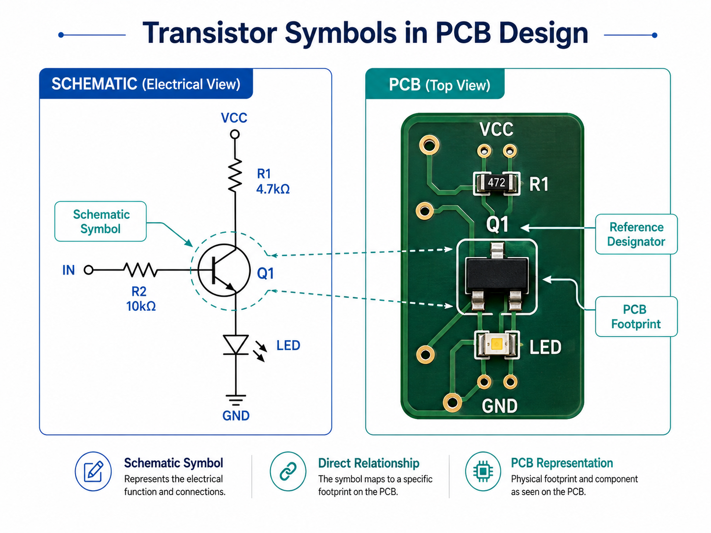
A transistor symbol in PCB work can appear in several places. It is usually seen in the schematic, component library, datasheet, silkscreen reference, and PCB assembly drawing.
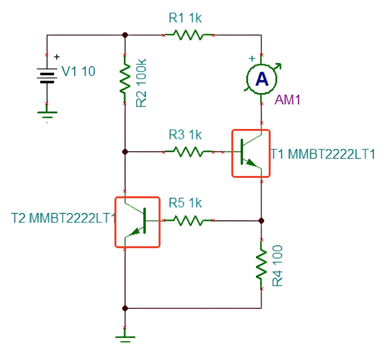
In a schematic, the transistor symbol shows the electrical function. For example, it may show whether the device is an NPN transistor used as a low-side switch, a PNP transistor used as a high-side switch, an NMOS transistor used for power control, or a PMOS transistor used for reverse polarity protection.
On the actual PCB, the symbol may not be drawn in full. Instead, the PCB normally uses a reference designator, such as Q1, Q2, Q3, or Q101. The letter “Q” is commonly used to identify transistors and transistor-like semiconductor devices.
PCB silkscreen may also show a small outline of the package. Common transistor packages include SOT-23, SOT-223, TO-92, TO-220, TO-252, TO-263, DFN, and QFN. The PCB footprint must match the actual component package and pin arrangement.
Transistor Symbol Pinout
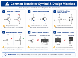
Transistor symbol pinout means the relationship between the schematic terminals and the physical pins of the transistor package. This is one of the most common sources of PCB design and repair mistakes.
For a BJT, the three pins are base, collector, and emitter. In the schematic symbol, these are easy to identify. However, on the physical part, the pin order depends on the package and manufacturer.
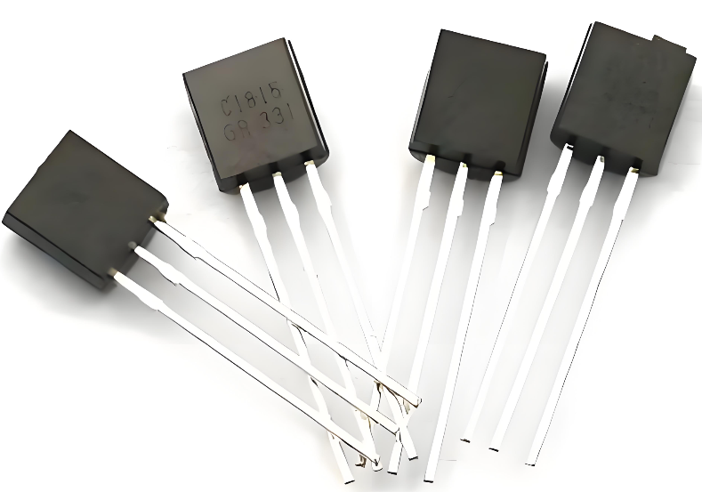
For example, a TO-92 transistor may have one of several pin arrangements, such as E-B-C, C-B-E, or E-C-B. A SOT-23 transistor may also vary depending on the exact part number.
For a MOSFET, the three pins are gate, drain, and source. In power packages such as TO-220 or DPAK, the tab is often connected to the drain, but this is not universal for every device type. Datasheet verification is still required.

What Are the Three Pins of a Transistor Called?
The three pins of a transistor depend on the transistor type.
For a BJT, the three pins are:
Base: The control pin. A small current applied to the base controls a larger current between collector and emitter.
Collector: The main current input terminal in many NPN circuits. It is usually connected to the load or supply side.
Emitter: The terminal where current leaves the transistor in a typical NPN configuration. It is often connected to ground in low-side switching circuits.
For a MOSFET, the three pins are:
Gate: The control pin. It uses voltage, rather than base current, to control the transistor.
Drain: One of the main current terminals. In an NMOS low-side switch, the drain is often connected to the load.
Source: The other main current terminal. In an NMOS low-side switch, the source is often connected to ground.
Although both BJTs and MOSFETs have three terminals, they are controlled differently. A BJT is current-controlled, while a MOSFET is voltage-controlled. This difference affects circuit design, driver selection, power loss, and switching speed.
What Is the Significance of Arrow in the Transistor Symbol?
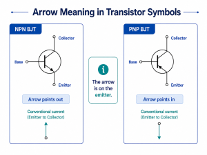
The arrow in a transistor symbol is very important. In a BJT symbol, the arrow is placed on the emitter and shows the direction of conventional current flow.
For an NPN transistor, the arrow points outward from the emitter. A simple way to remember this is: NPN means Not Pointing iN.
For a PNP transistor, the arrow points inward toward the base. This means the current direction is different from an NPN transistor.
| Type | Arrow Direction | Basic Meaning |
|---|---|---|
| NPN | Arrow points out | Current flows from collector to emitter when turned on |
| PNP | Arrow points in | Current flows from emitter to collector when turned on |
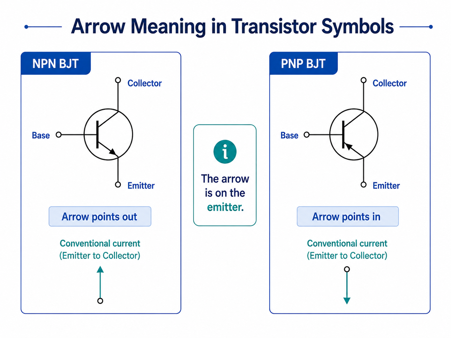
The arrow also helps technicians identify transistor polarity in a schematic. This matters when replacing components, testing circuits, or checking switching paths.
What Are the Two Major Types of Transistors?
The two major types of transistors are BJT and FET.
BJT stands for Bipolar Junction Transistor. It uses both electrons and holes for conduction. BJT devices are commonly used for signal amplification, switching, audio circuits, and general-purpose control circuits. The two main BJT types are NPN and PNP.
FET stands for Field-Effect Transistor. It controls current through an electric field. The most common FET used in PCB design is the MOSFET, which stands for Metal-Oxide-Semiconductor Field-Effect Transistor. MOSFETs are widely used in power switching, motor drivers, battery protection circuits, DC-DC converters, and logic-level control circuits.
| Category | Main Types | Control Method | Common Use |
|---|---|---|---|
| BJT | NPN, PNP | Base current | Amplification and small-signal switching |
| FET | NMOS, PMOS, JFET | Gate voltage | Power switching and high-input impedance circuits |
In modern PCB design, MOSFETs are very common because they can switch efficiently, handle high current, and work well with microcontroller outputs when properly selected. BJTs are still widely used where simple biasing, low cost, linear gain, or predictable small-signal behavior is needed.
Why Are Transistors Called NPN or PNP?
NPN and PNP names describe the semiconductor layer structure inside a BJT.
An NPN transistor has a thin P-type region between two N-type regions. The three regions form the collector, base, and emitter. In many low-voltage electronic circuits, NPN transistors are used as low-side switches because they are easy to drive from microcontrollers or logic circuits.
A PNP transistor has a thin N-type region between two P-type regions. PNP transistors are often used for high-side switching, signal control, and complementary amplifier circuits.
| Type | Internal Structure | Common Switching Position |
|---|---|---|
| NPN | N-P-N | Low-side switching |
| PNP | P-N-P | High-side switching |
The naming is not just theoretical. It directly affects how the transistor is biased. An NPN transistor turns on when the base is at a higher voltage than the emitter by about 0.6–0.7 V for silicon devices. A PNP transistor turns on when the base is lower than the emitter by about 0.6–0.7 V.
This difference is why NPN and PNP transistor symbols must not be confused. Replacing one with the other will usually make the circuit fail or behave incorrectly.
Can I Use an NPN Transistor as a Switch?
Yes, an NPN transistor can be used as a switch. This is one of the most common uses of an NPN transistor in PCB circuits.
A typical NPN switching circuit works as a low-side switch. The load is connected between the positive supply and the collector. The emitter is connected to ground. When enough base current flows, the transistor turns on and allows current to pass from collector to emitter.
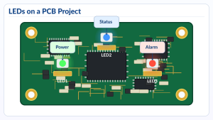
Common loads controlled by NPN transistor switches include LEDs, relays, buzzers, small motors, optocouplers, and signal lines.
A basic NPN switching circuit normally needs:
| Part | Purpose |
|---|---|
| NPN transistor | Controls the load |
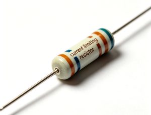
| Base resistor | Limits base current |
| Load | LED, relay, buzzer, or other device |
| Flyback diode | Protects transistor when driving inductive loads |
| Pull-down resistor | Keeps transistor off when input is floating |
For relay and motor circuits, a flyback diode is especially important. Without it, voltage spikes from the coil may damage the transistor.
When using an NPN transistor as a switch, the designer must check collector current, collector-emitter voltage, base current, power dissipation, saturation voltage, package thermal performance, and PCB copper area. For high-current switching, a logic-level NMOS transistor may be a better choice because it usually has lower conduction loss.
How Much Voltage Does a Transistor Need?
The voltage a transistor needs depends on its type and how it is used.
For a silicon BJT, the base-emitter junction usually starts conducting at about 0.6–0.7 V. However, this does not mean every BJT circuit only needs 0.7 V. The full circuit must provide enough voltage and current to drive the load.
For a BJT used as a switch, the base must receive enough current to drive the transistor into saturation. The base resistor must be calculated based on input voltage, base-emitter voltage, load current, and required gain margin.
For a MOSFET, the gate voltage controls conduction. A MOSFET has a parameter called gate threshold voltage, often written as VGS(th). However, this value only indicates when the MOSFET starts to conduct a very small current. It does not mean the MOSFET is fully on.
For practical switching, designers should check the MOSFET’s RDS(on) at the actual gate drive voltage. For example, if a microcontroller outputs 3.3 V, the MOSFET should have a low RDS(on) specified at 2.5 V or 3.3 V, not only at 10 V.
| Transistor Type | Control Requirement | Design Note |
|---|---|---|
| BJT | Base-emitter voltage plus base current | Needs a base resistor |
| NMOS | Gate-source voltage | Check RDS(on) at real drive voltage |
| PMOS | Gate-source voltage, usually negative relative to source | Often used in high-side circuits |
Voltage selection should always consider the supply voltage, signal level, load current, temperature, and safety margin.
How Do You Test If a Transistor Is Working?
A transistor can be tested with a multimeter, component tester, or circuit-level measurement. The best method depends on whether the transistor is removed from the PCB or still soldered on the board.
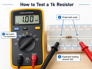
For a BJT, a digital multimeter in diode mode can check the base-emitter and base-collector junctions. An NPN transistor behaves like two diodes sharing the base. A normal silicon junction often shows a forward voltage drop around 0.6–0.7 V. A PNP transistor is tested with reversed probe polarity.
Basic BJT test signs:
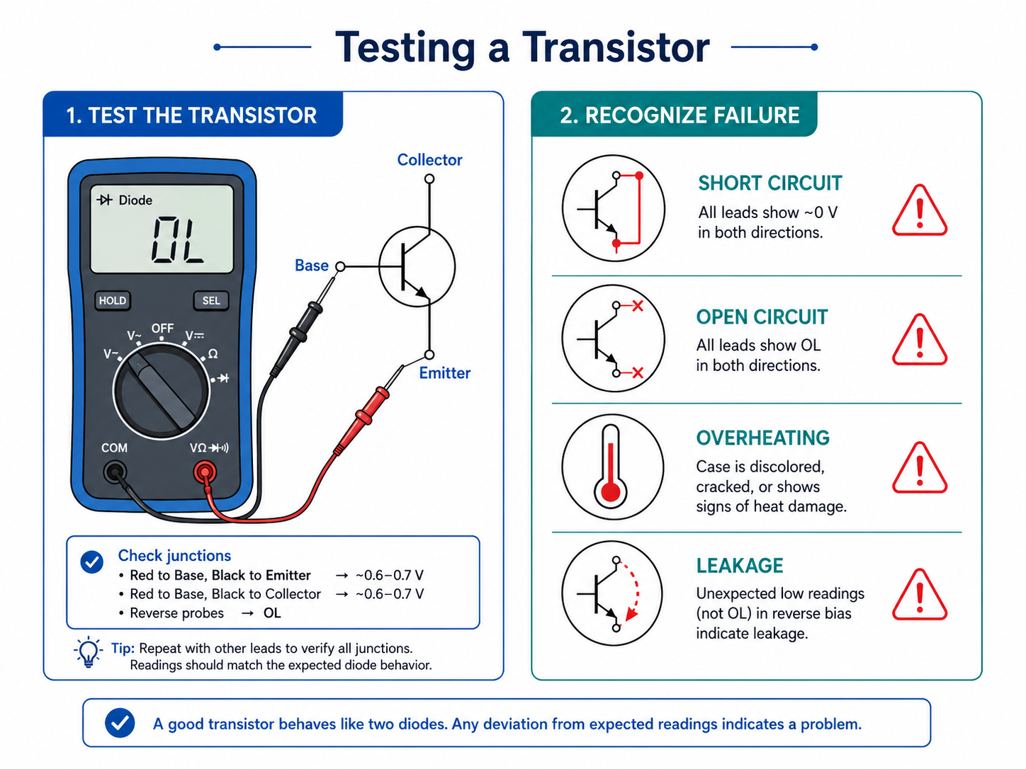
For a MOSFET, testing is different. A multimeter can check for drain-source shorts and body diode behavior. Some MOSFETs can also be briefly charged at the gate to see if the channel turns on, but this method must be used carefully because MOSFET gates can be damaged by static electricity.
When the transistor is still on a PCB, surrounding components may affect readings. Resistors, diodes, IC pins, coils, or capacitors connected to the same circuit can create misleading results. If the measurement is unclear, lifting one pin or removing the transistor gives a more reliable test.
In production PCB assembly, transistor testing may also include AOI, X-ray for hidden joints, in-circuit testing, functional testing, and thermal inspection under load.
What Is a Transistor Used For?
A transistor is used to control electrical current. Its two major functions are switching and amplification.
In switching circuits, a transistor works like an electronic on/off control. It can allow a low-power signal from a microcontroller to control a larger load. This is common in LED control, relay drivers, motor drivers, power enable circuits, battery management systems, and digital output stages.
In amplification circuits, a transistor increases the strength of a small signal. This is used in audio amplifiers, RF circuits, sensor interfaces, analog front ends, and signal conditioning circuits.
Common transistor applications include:
| Application | Typical Transistor Role |
|---|---|
| LED driver | Controls LED current |
| Relay driver | Switches relay coil current |
| Audio amplifier | Amplifies weak audio signals |
| Power supply | Supports regulation and switching |
| Motor control | Drives or modulates motor current |
| Battery circuit | Provides protection or switching |
| Logic interface | Converts or buffers signals |
| RF circuit | Amplifies high-frequency signals |
| Sensor circuit | Conditions small analog signals |
In PCB design, transistors are often small but critical. A single wrong transistor selection may cause overheating, unstable switching, weak drive strength, leakage current, voltage drop, or signal distortion.
For this reason, engineers should select transistors based on real working conditions, not only package size or price. Important parameters include voltage rating, current rating, gain, threshold voltage, RDS(on), switching speed, leakage current, power dissipation, thermal resistance, and package availability.
What Happens When a Transistor Fails?
When a transistor fails, the circuit may stop working, work intermittently, overheat, draw too much current, or produce incorrect output signals. The exact symptom depends on the failure mode.
A transistor may fail as a short circuit, open circuit, leakage path, degraded gain, unstable switching device, or thermally damaged part.
| Failure Mode | Common Symptom |
|---|---|
| Shorted collector-emitter or drain-source | Load stays on, fuse blows, power rail drops |
| Open internal junction | Load never turns on |
| Excessive leakage | Circuit behaves unpredictably |
| Reduced gain | Weak switching or low amplification |
| Gate oxide damage in MOSFET | Device cannot switch correctly |
| Thermal damage | Burn marks, discoloration, repeated failure |
Common causes of transistor failure include overcurrent, overvoltage, electrostatic discharge, wrong pinout, poor heat dissipation, insufficient base/gate drive, inductive voltage spikes, soldering damage, and incorrect replacement parts.
On a PCB, transistor failure may also be caused by design issues. For example, a relay driver without a flyback diode can repeatedly stress the transistor. A MOSFET with insufficient gate voltage may operate in a partially on state and overheat. A BJT without a proper base resistor may draw excessive current from the control circuit.
When troubleshooting, do not only replace the failed transistor. It is better to check the load, driver signal, surrounding resistors, protection diodes, PCB solder joints, and power supply behavior. If the root cause remains, the new transistor may fail again.