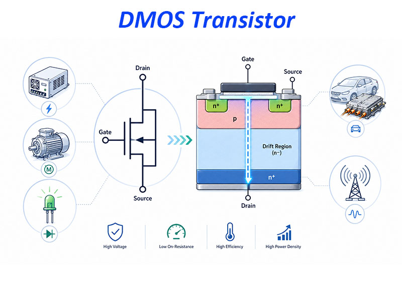
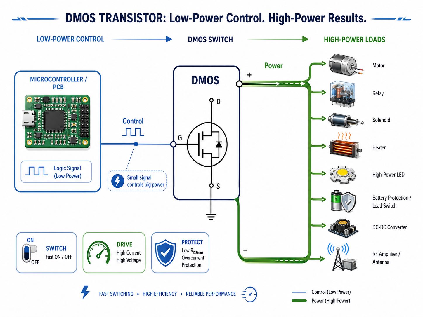
A DMOS transistor is a special type of MOSFET designed for power control, fast switching, and higher voltage operation. If a small signal transistor is like a small tap controlling a thin stream of water, a DMOS transistor is more like a strong electronic valve. It allows a small control signal to manage a much larger current in a circuit.
DMOS stands for double-diffused metal-oxide-semiconductor. The name sounds technical, but the basic idea is not difficult. A DMOS transistor uses a special internal structure to create a short channel and a voltage-supporting drift region. The short channel helps the transistor switch quickly. The drift region helps the device withstand higher voltage when it is turned off.
This makes DMOS transistors useful in power supplies, motor drivers, automotive electronics, LED drivers, battery protection circuits, industrial control boards, and RF power circuits. For PCB and PCBA projects, understanding DMOS transistors is helpful because these components often sit near high-current paths, switching nodes, heat-generating loads, and power-control areas.
What Is a DMOS Transistor?
A DMOS transistor is a MOSFET built with a double-diffused structure. In plain language, it is a voltage-controlled transistor that allows current to flow between drain and source when the gate voltage is applied correctly.
A basic MOSFET has three important terminals:
| Terminal | Simple Meaning | What It Does |
|---|---|---|
| Gate | Control pin | Turns the transistor on or off |
| Drain | Output current path | Current usually enters or leaves here, depending on circuit type |
| Source | Reference current path | Often connected to ground or a supply rail |
| Body / Substrate | Internal semiconductor base | Supports the device structure |
In a MOSFET, the gate is insulated from the current path by a thin oxide layer. When voltage is applied to the gate, it creates an electric field. This electric field forms a channel between source and drain, allowing current to flow.
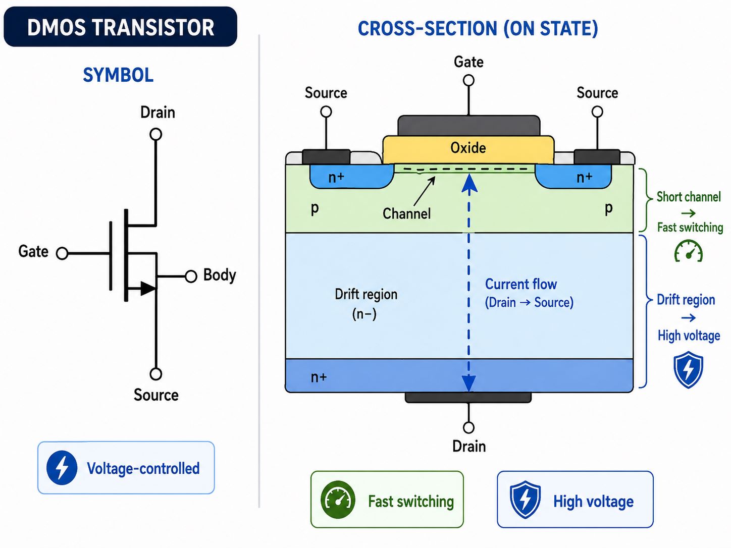
A DMOS transistor follows the same basic MOSFET idea, but its internal structure is optimized for power. The “double-diffused” part helps define a short channel and a drift region. The short channel supports fast switching, while the drift region helps the transistor block higher voltage when it is turned off.
The easiest definition is this:
A DMOS transistor is a power-oriented MOSFET structure that uses double diffusion to achieve fast switching, high voltage capability, and efficient current control.
What Does a DMOS Transistor Do?
A DMOS transistor mainly works as an electronic switch. It can turn current on and off quickly without needing much input power at the gate.
Think of a microcontroller on a PCB. The microcontroller pin may only provide a small control signal. It cannot directly drive a motor, solenoid, relay, heater, or high-power LED. A DMOS transistor can sit between the control signal and the load. The control signal tells the gate what to do, and the DMOS transistor handles the heavier current.
In real circuits, a DMOS transistor can:
| Function | Easy Explanation | Common Example |
|---|---|---|
| Switch current | Turns a load on or off | Motor driver, relay driver |
| Control power | Helps regulate voltage or current | DC-DC converter |
| Drive loads | Handles current for external parts | LED module, solenoid |
| Protect circuits | Used in power management and protection paths | Battery protection, load switch |
| Amplify RF power | Used in certain RF power stages | ISM, broadcast, communication equipment |
The key point is simple:
A DMOS transistor lets a low-power control signal manage a higher-power circuit.
This is why it is common in power electronics and embedded control systems.
How Does a DMOS Transistor Work?
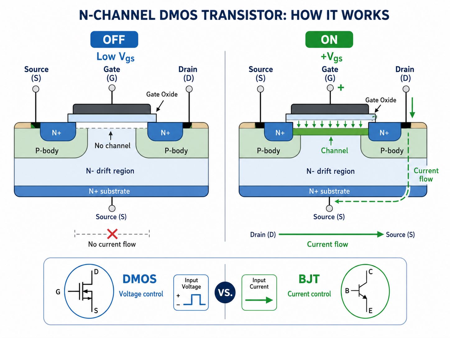
A DMOS transistor works by using voltage at the gate to control the current path between drain and source.
When the gate voltage is too low, the transistor is off. The path between drain and source is blocked, so current cannot flow through the main channel. When the gate voltage rises above the required level, a channel forms near the surface of the semiconductor. This channel allows current to pass.
You can imagine the gate as a door handle. The drain and source are like two rooms. Without the correct gate voltage, the door stays closed. When the gate voltage is high enough, the door opens and current can move through.
For an N-channel DMOS transistor, which is very common in power circuits:
- A positive gate-to-source voltage is applied.
- An electric field forms under the gate oxide.
- A conductive channel appears.
- Current flows between drain and source.
- When the gate voltage is removed, the channel disappears.
This is different from a bipolar transistor, such as an NPN transistor. A BJT needs base current to stay on. A MOSFET, including DMOS, is controlled mainly by voltage.
This difference matters in switching circuits. Because the gate does not need continuous drive current in the same way a BJT base does, DMOS transistors can be easier to drive. They are also useful in high-frequency switching because MOSFETs avoid some of the storage-delay problems found in bipolar devices.
DMOS Transistor Structure: What Makes It Different?
The structure is the main reason a DMOS transistor is useful. A normal MOSFET can switch signals, but a DMOS transistor is built to manage power more effectively.
The most important parts inside a DMOS transistor are:
| Structure Part | Simple Role |
|---|---|
| Gate oxide | Insulates the gate and allows electric-field control |
| Gate electrode | Receives the control voltage |
| Source region | Provides one side of the current path |
| Body region | Helps form the channel |
| Drift region | Supports high voltage when the device is off |
| Drain region | Provides the other side of the current path |
The drift region is especially important. In a high-voltage transistor, the device must survive voltage stress when it is off. The drift region spreads the electric field and helps prevent breakdown.
This creates one of the classic power MOSFET trade-offs:
Higher breakdown voltage usually needs a stronger drift region, but that can increase resistance. Lower resistance improves efficiency, but the device still needs enough voltage strength.
This is why datasheets matter. Two DMOS transistors may look similar from the outside, but their internal structures can be tuned for different voltage, current, switching speed, and thermal behavior.
What Are the Main Characteristics of a DMOS Transistor?
When engineers choose a DMOS transistor, they do not only look at the package size. They check electrical and thermal parameters to make sure the device can work safely in the real circuit.
- Breakdown voltage: This tells you how much voltage the transistor can block when it is off. If the circuit voltage is higher than the transistor can handle, the device may fail. A 12V system, for example, should not automatically use a 12V-rated transistor. Designers usually leave margin for spikes, surges, and switching noise.
- On-resistance: On-resistance is often shown as RDS(on). It tells you how much resistance exists between drain and source when the transistor is fully on. Lower RDS(on) usually means less heat and better efficiency. In power circuits, this is one of the most important selection points.
- Gate threshold voltage: Gate threshold voltage tells you when the transistor just begins to turn on. It does not mean the transistor is fully on. This is a common beginner mistake. For switching applications, you should check RDS(on) at the actual gate voltage used in your circuit.
- Switching speed: DMOS transistors can switch quickly. This makes them useful in DC-DC converters, power supplies, and motor control. However, fast switching also makes PCB layout more important. Poor layout can cause ringing, EMI, and heat concentration.
- Capacitance and gate charge: The gate behaves partly like a small capacitor. To switch the transistor on and off, the driver must charge and discharge this gate. Higher gate charge can make switching slower or require a stronger driver.
- Thermal performance: A DMOS transistor may handle high current on paper, but real performance depends on heat removal. PCB copper area, thermal vias, package type, airflow, and ambient temperature all affect reliability.
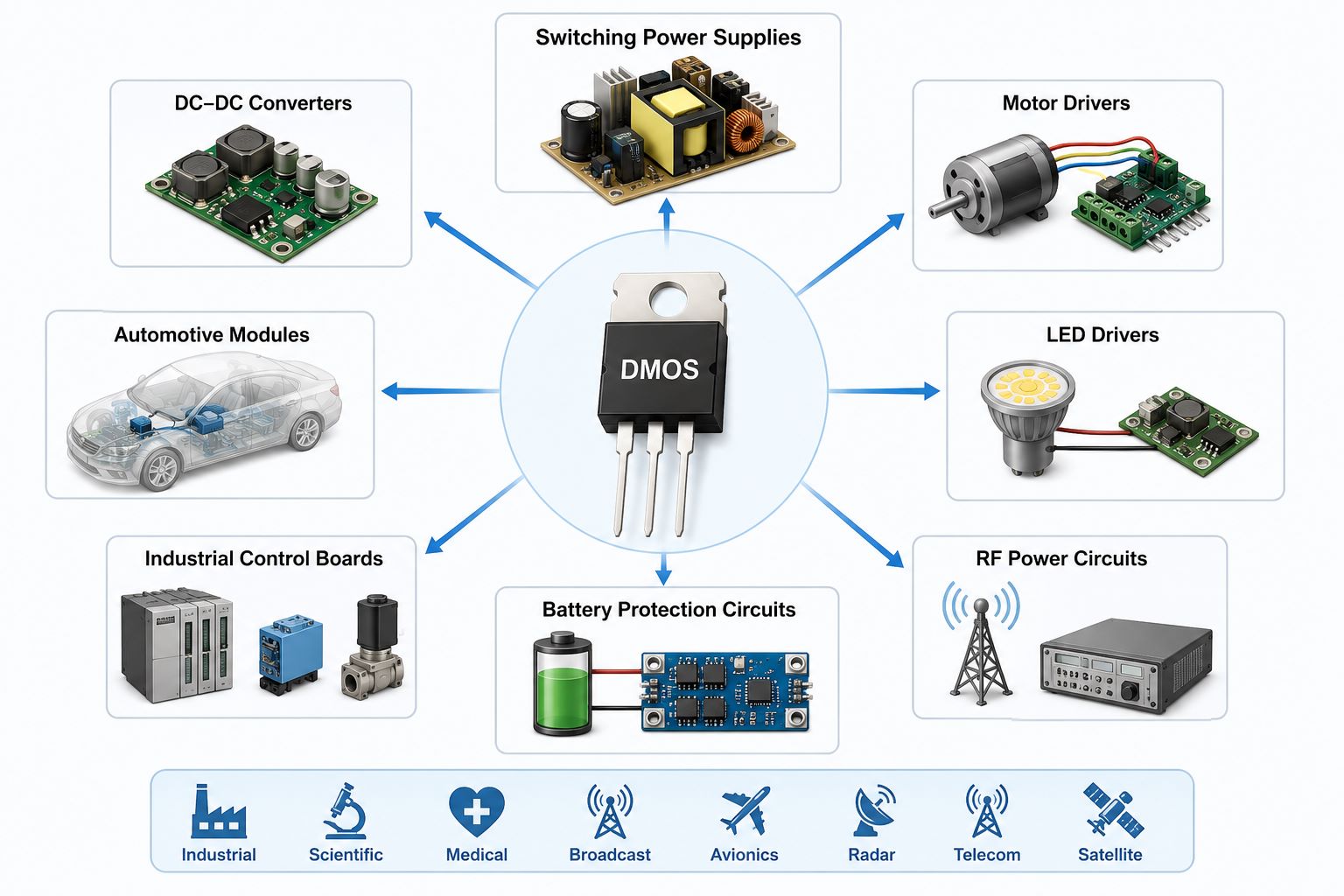
Where Are DMOS Power Transistors Used?
DMOS power transistors are used wherever circuits need efficient switching, power control, or high-speed current handling.
Common applications include:
| Application | Why DMOS Is Useful |
|---|---|
| Switching power supplies | Fast switching and efficient current control |
| DC-DC converters | Helps step voltage up or down efficiently |
| Motor drivers | Controls current to motors |
| Automotive modules | Handles loads in body, lighting, and power systems |
| LED drivers | Controls current for high-power LEDs |
| Industrial control boards | Drives relays, valves, solenoids, and actuators |
| Battery protection circuits | Switches charging and discharging paths |
| RF power circuits | Supports certain high-frequency power applications |
In RF applications, DMOS and LDMOS devices can be used in industrial, scientific, medical, broadcast, avionics, radar, telecom, and satellite communication equipment.
For PCB and PCBA projects, DMOS transistors are often found near power inputs, inductors, transformers, motors, connectors, and heat-generating loads. If you see a power device connected to a large copper area, a heat sink, or a switching node, there is a good chance it is handling serious current-control work.
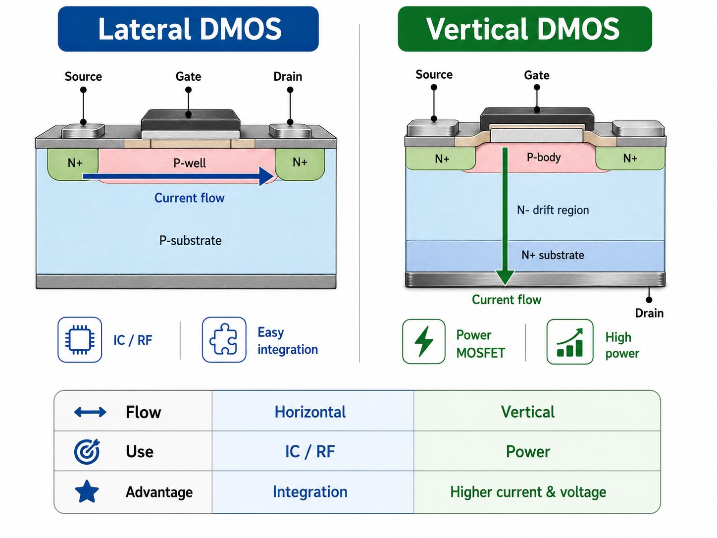
Lateral DMOS Transistor vs Vertical DMOS Transistor: What Is the Difference?
DMOS transistors can be built in different layouts. The two important terms are lateral and vertical.
- A lateral DMOS transistor allows current to flow mostly along the surface of the chip. The source, gate, and drain are usually arranged on the top side. This structure is useful for integrated circuits and certain RF applications.
- A vertical DMOS transistor allows current to flow vertically through the chip. The source and gate are often on the top side, while the drain is on the backside. This structure is common in discrete power MOSFETs because it supports higher voltage and current.
Here is the simple comparison:
| Type | Current Flow | Common Use | Main Advantage |
|---|---|---|---|
| Lateral DMOS / LDMOS | Mostly horizontal | ICs, RF devices, integrated power circuits | Easier integration, good RF behavior |
| Vertical DMOS | Vertical through the die | Discrete power MOSFETs | Better for higher current and voltage |
For a beginner, the easiest way to remember it is this:
Lateral devices are easier to integrate. Vertical devices are often better for handling larger power.
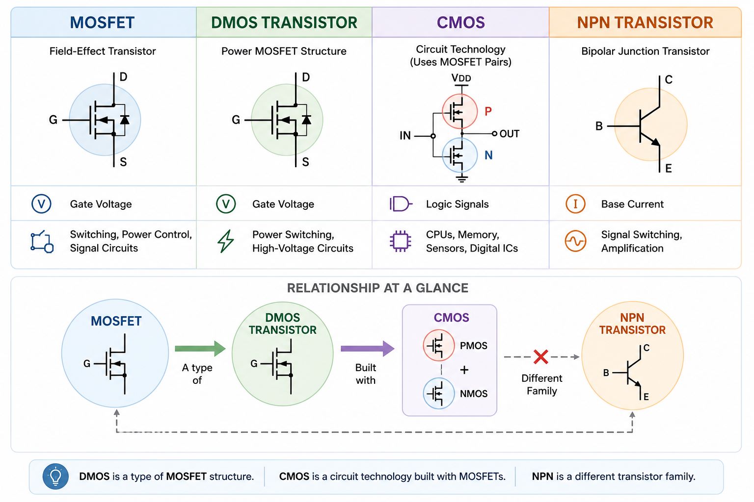
DMOS Transistor vs MOSFET vs CMOS vs NPN Transistor
These terms are often mixed together, so it helps to separate them clearly.
A MOSFET is a general type of transistor controlled by gate voltage. A DMOS transistor is a special MOSFET structure designed for power use. CMOS is not one transistor. It is a circuit technology that uses complementary MOSFETs, usually NMOS and PMOS, to build digital circuits. An NPN transistor is a type of bipolar transistor controlled by base current.
| Term | What It Is | Controlled By | Typical Use |
|---|---|---|---|
| MOSFET | A field-effect transistor | Gate voltage | Switching, power control, signal circuits |
| DMOS transistor | A power MOSFET structure | Gate voltage | Power switching, high-voltage circuits |
| CMOS | A circuit technology using MOSFET pairs | Logic signals | CPUs, memory, sensors, digital ICs |
| NPN transistor | A bipolar junction transistor | Base current | Signal switching, amplification |
The relationship is simple:
DMOS is a type of MOSFET structure. CMOS is a circuit technology built with MOSFETs. NPN is a different transistor family.
This distinction matters when reading datasheets or discussing PCB design. If someone says “MOSFET,” they may be speaking broadly. If someone says “DMOS,” they are usually talking about a power-oriented MOSFET structure. If someone says “CMOS,” they are usually talking about logic IC technology, not a single discrete transistor.
DMOS Transistor Circuit, Schematic, and Symbol: What Should Engineers Know?
In a schematic, a DMOS transistor usually looks similar to a MOSFET symbol. The symbol shows gate, drain, and source. Some symbols also show the body diode, which is important in power circuits.
The body diode is not an optional external diode. It is part of the MOSFET structure. In some circuits, it helps provide a current path. In other circuits, it may create unwanted conduction if the design is wrong.
A common DMOS transistor circuit is a low-side switch.
In this circuit:
- The load connects to the positive supply.
- The DMOS transistor sits between the load and ground.
- The gate receives a control signal.
- When the gate turns on, current flows through the load.
- When the gate turns off, current stops.
This setup is common for LEDs, relays, fans, small motors, and solenoids.
Another common design is a high-side switch. In this case, the transistor sits between the power supply and the load. High-side switching is useful when the load must stay connected to ground, but the gate drive is usually more complex.
For PCB layout, the schematic is only half the story. A good DMOS circuit also needs careful copper design. High-current paths should be short and wide. Switching loops should be compact. Gate traces should avoid noise. Thermal vias and copper pours may be needed for heat spreading.
In power circuits, a poor layout can make a good transistor behave badly.
How to Choose the Right DMOS Transistor for a Circuit
Choosing a DMOS transistor is not about picking the part with the highest current rating. Datasheet current ratings are often measured under ideal conditions. Real PCB conditions are different.
- Check voltage rating: Choose a drain-source voltage rating higher than your maximum circuit voltage. Add margin for spikes and transients. For example, a 24V system may need a 40V, 60V, or higher-rated part, depending on the environment.
- Check current rating: Look at both continuous current and pulse current. Then check whether the PCB and package can actually remove the heat.
- Check RDS(on): Lower RDS(on) reduces conduction loss. This is important when the transistor stays on for long periods or carries high current.
- Check gate drive voltage: Make sure your control circuit can fully turn the transistor on. A 5V microcontroller may not fully drive every power transistor. A 3.3V microcontroller needs even more attention.
- Check switching requirements: For high-frequency switching, look at gate charge, input capacitance, output capacitance, and reverse transfer capacitance. These values affect switching loss and driver selection.
- Check thermal path: Look at package thermal resistance, PCB copper area, airflow, and expected ambient temperature. Heat is one of the most common reasons power devices fail.
- Check application conditions: Motor loads, inductors, relays, and solenoids can create voltage spikes. The design may need flyback diodes, TVS diodes, snubbers, or proper gate protection.
A good rule is this:
Do not select a DMOS transistor only by voltage and current. Select it by voltage, current, resistance, gate drive, switching speed, thermal design, and load behavior.
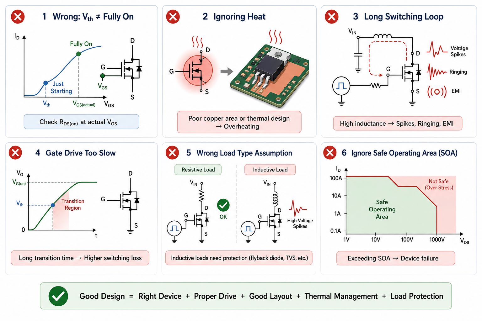
Common Mistakes When Using DMOS Transistors
Many DMOS transistor problems come from simple design mistakes. The device itself may be good, but the circuit around it may not support it properly.
Mistake 1: Confusing threshold voltage with full turn-on voltage
- The threshold voltage only means the transistor starts to conduct a tiny current. It does not mean it is ready to carry the full load current.
- Always check RDS(on) at your actual gate voltage.
Mistake 2: Ignoring heat
- A transistor with low resistance still produces heat. If the PCB has poor copper area or weak thermal design, the device may overheat.
Mistake 3: Using long switching loops
- Long current loops increase inductance. This can cause voltage spikes, ringing, EMI, and unstable behavior.
Mistake 4: Driving the gate too slowly
- A slow gate signal keeps the transistor in its transition region for too long. During this time, voltage and current overlap, creating extra switching loss.
Mistake 5: Forgetting the load type
- Inductive loads behave differently from resistive loads. Motors, coils, relays, and transformers can produce high voltage spikes when current changes quickly.
Mistake 6: Not reading the safe operating area
- The safe operating area, or SOA, shows what voltage and current combinations the device can survive for a certain time. This matters in linear operation, startup, fault conditions, and pulse loads.
- Good engineering is not only about choosing a strong transistor. It is about making sure the whole circuit gives that transistor a safe working environment.
FAQs About DMOS Transistor
Q1: Is a DMOS transistor the same as a MOSFET?
A DMOS transistor is a type of MOSFET structure. All DMOS transistors are MOSFET-based, but not all MOSFETs are DMOS. DMOS is usually used when the device is designed for power handling.
Q2: Why is it called double-diffused?
It is called double-diffused because two diffusion steps are used to form important internal regions of the transistor. These diffusions help define the channel length and support the power structure.
Q3: Can a DMOS transistor be used as a switch?
Yes. Switching is one of its most common uses. It can control motors, LEDs, relays, solenoids, and power conversion circuits.
Q4: What is the main advantage of a DMOS transistor?
The main advantage is efficient power switching. It can handle useful voltage and current while being controlled by gate voltage.
Q5: What is the difference between DMOS and LDMOS?
DMOS is a broader double-diffused MOS structure. LDMOS means laterally diffused MOS and is often used in RF and integrated power applications. LDMOS current flow is mainly lateral, while many power DMOS devices have strong vertical current flow.
Q6: Is DMOS better than an NPN transistor?
It depends on the circuit. For many power switching tasks, DMOS can be easier to drive and more efficient. For some analog or low-cost signal circuits, an NPN transistor may still be suitable.
Q7: What does RDS(on) mean in a DMOS transistor?
RDS(on) is the resistance between drain and source when the transistor is on. Lower RDS(on) usually means less heat and better efficiency.
Q8: Why does PCB layout matter for DMOS transistors?
Because DMOS transistors often switch high current quickly. Poor layout can create heat, noise, voltage spikes, and EMI. Good copper design and short current paths improve reliability.
All in all, a DMOS transistor may sound difficult at first, but its basic job is easy to understand. It is a power-focused MOSFET structure that uses gate voltage to control current. Its double-diffused design helps create a short channel, while its drift region supports higher voltage. This combination makes it useful in switching power supplies, automotive electronics, motor drivers, LED drivers, RF circuits, and industrial control systems.
For PCB and PCBA projects, the transistor itself is only one part of the design. The board must also support current flow, heat dissipation, switching stability, and long-term reliability. At Best Technology, we support customers with PCB manufacturing and assembly for power electronics, automotive modules, industrial control boards, LED applications, and other electronic products. If your project uses DMOS transistors, MOSFETs, power ICs, or high-current circuits, our engineering team can help review manufacturability, copper design, assembly requirements, and production quality before the design moves into batch manufacturing. For inquiries or project discussions, please feel free to contact us at sales@bestpcbs.com.