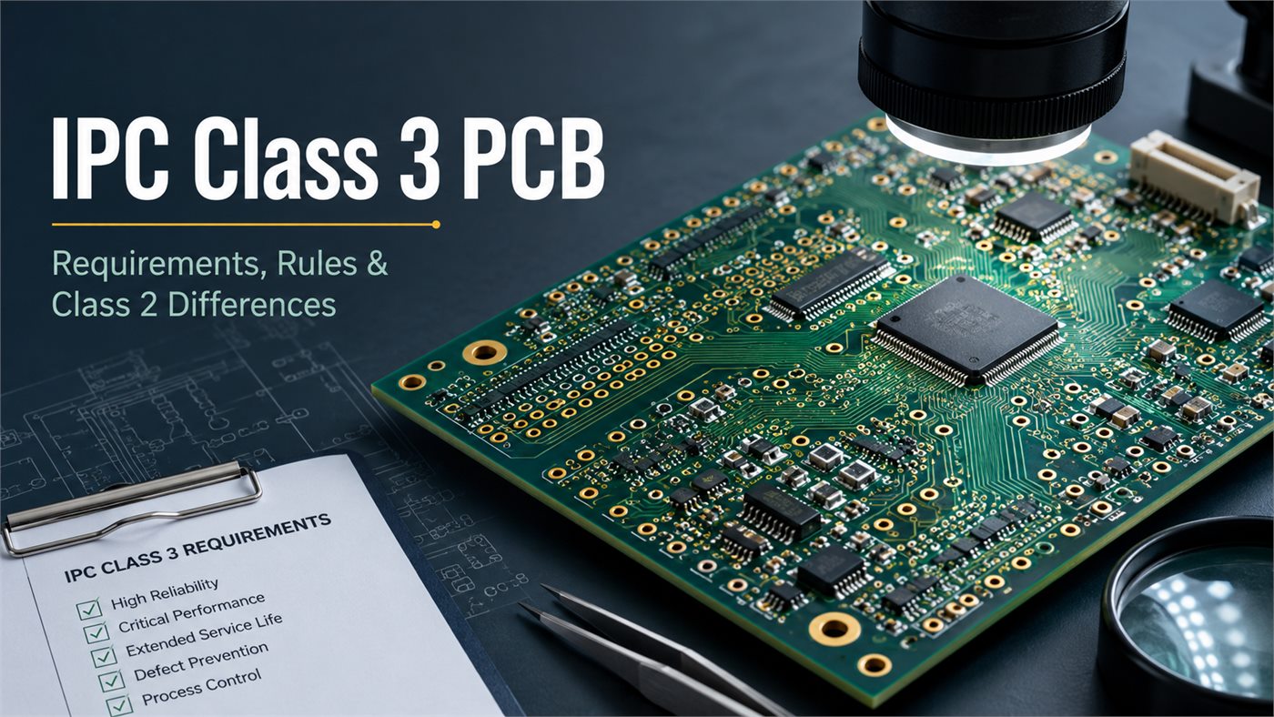
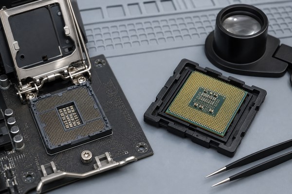
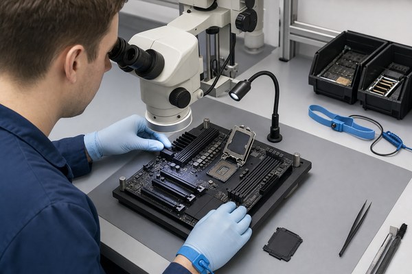
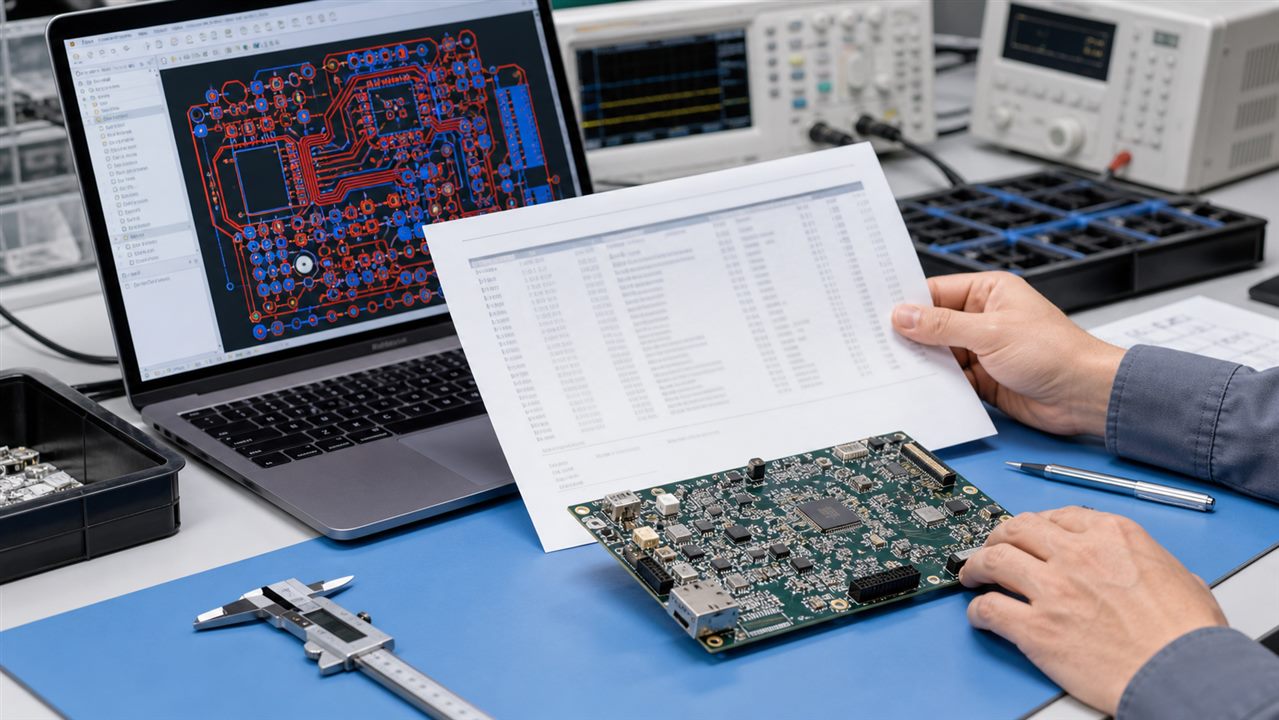
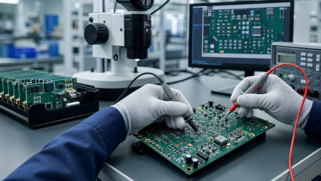
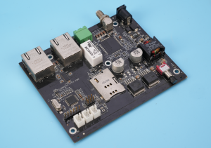
IC board components are the electronic parts mounted on a printed circuit board to make a circuit perform its required function. They include integrated circuits, resistors, capacitors, diodes, transistors, inductors, connectors, crystals, sensors, switches, protection devices, and power components.
Component selection affects circuit stability, PCB design layout, assembly yield, product lifetime, testing cost, and mass production risk. A well-designed IC board uses the right components, correct footprints, suitable materials, reliable soldering processes, and proper quality control.
What Are IC Board Components?
IC board components are the parts assembled on a PCB to create a working electronic circuit. The PCB provides copper traces, pads, vias, solder mask, and mechanical support. The components provide control, power conversion, signal processing, protection, sensing, communication, or user interface functions.
The integrated circuit, or IC, is usually the main functional device on the board. It may be a microcontroller, memory chip, power management IC, driver IC, amplifier, logic IC, or communication chip. After these components are soldered onto the PCB, the finished product is usually called a PCBA, or printed circuit board assembly.
Why Are IC Board Components Important?
IC board components directly decide how the product works in real conditions. A wrong capacitor may cause unstable power. A poor connector may fail after vibration. A MOSFET with weak thermal margin may overheat. A counterfeit IC may pass basic inspection but fail during long-term use.
In mass production, components also affect cost and delivery. Some ICs have long lead times, limited alternatives, or strict storage requirements. If the BOM is not reviewed early, a prototype may work, but batch production may become expensive, unstable, or delayed.
How Do IC Board Components Work Together?
An IC board works through coordinated electrical paths. Power enters the board through a connector, terminal, battery contact, USB port, or power jack. Protection parts such as fuses, TVS diodes, ESD arrays, or common-mode chokes help reduce electrical stress.
Power management parts then convert and regulate voltage. For example, a DC-DC converter may work with a MOSFET, diode, inductor, capacitor, and feedback resistor network. These parts create stable power rails for ICs and other devices.
Signal components handle communication between ICs, sensors, memory, displays, motors, or external systems. Passive components such as resistors and capacitors support filtering, timing, voltage division, current limiting, and noise control. Here is a basic workflow:
Main Types of IC Board Components
Different IC board components serve different electrical and mechanical roles. The table below gives a practical overview.
Component Type
Common Examples
Main Function
Key Selection Point
Integrated circuits
MCU, memory, driver IC, PMIC
Control, logic, processing, conversion
Package, voltage, temperature, lifecycle
Resistors
Chip resistor, current sense resistor
Current limiting, feedback, voltage division
Value, tolerance, power rating
Capacitors
MLCC, electrolytic, tantalum
Decoupling, filtering, energy storage
Capacitance, voltage, ESR, temperature behavior
Inductors
Power inductor, ferrite bead
Energy storage, EMI control
Current rating, DCR, saturation current
Diodes
Schottky, TVS, Zener, LED
Rectification, protection, indication
Voltage, current, response time
Transistors
MOSFET, BJT, IGBT
Switching, amplification, power control
Current, voltage, RDS(on), heat dissipation
Connectors
Board-to-board, wire-to-board, terminal block
Electrical interface
Pitch, current rating, plating, mating cycle
Timing parts
Crystal, oscillator, resonator
Clock generation
Frequency tolerance, load capacitance
Protection parts
Fuse, PTC, ESD array
Circuit safety
Surge rating, clamping voltage
Electromechanical parts
Relay, switch, buzzer
User or load interface
Contact rating, mechanical life
Common IC Packages and Mounting Methods
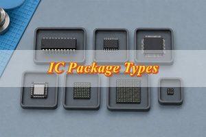
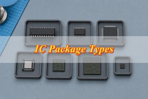
IC packages affect PCB size, routing difficulty, soldering quality, heat dissipation, and inspection method. Common packages include SOIC, SOP, QFN, QFP, BGA, LGA, DFN, SOT, DIP, and TO packages.
Most modern IC boards use SMT assembly because surface mount components are compact and suitable for automated production. Through-hole components are still used for connectors, relays, transformers, large capacitors, and parts that need stronger mechanical support.
Materials Used in IC Board Components and PCBs
IC board components use different materials based on function. IC packages may include silicon dies, copper lead frames, bonding wires, epoxy molding compound, solder balls, and plated terminals. Passive components may use ceramic, metal film, carbon film, ferrite, aluminum foil, polymer, or magnetic core materials.
The PCB substrate is also important. Standard consumer electronics often use normal FR4, High-temperature, high-power, RF, automotive, LED, or power module applications may require high-Tg FR4, aluminum PCB, copper base PCB, ceramic PCB, Rogers material like RO4350B, RO4003C, RT5880, , or hybrid stackups.
For example, a high-power MOSFET on FR4 may need large copper pours and thermal vias. A high-brightness LED may need aluminum or ceramic substrate for better heat spreading. A high-frequency IC may need low-loss material and controlled impedance.
IC Board Component Applications
IC board components are used in almost every electronic product, but each market has different priorities. The most common applications including:
Consumer electronics – MCU, charger IC, LEDs, USB connector
Industrial control – Relays, isolators, terminal blocks, TVS diodes
A smart home board may focus on compact layout and cost control. An EV charger, medical controller, or industrial power board needs stronger derating, testing, and documentation.
Testing Methods and Quality Standards
Common inspection methods include visual inspection, AOI, X-ray, in-circuit testing, flying probe testing, power-on testing, firmware programming, functional testing, burn-in, and thermal testing.
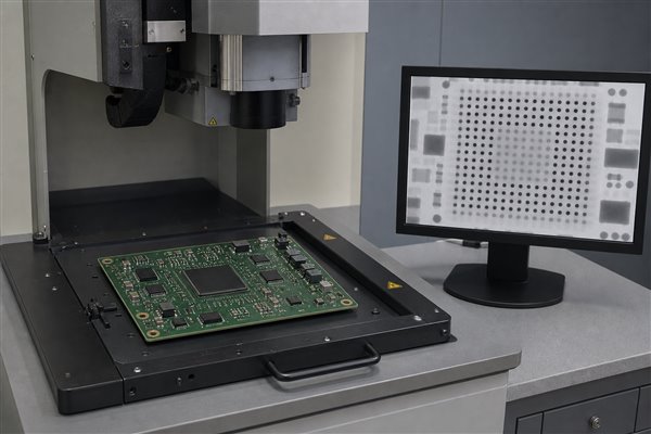
BGA, LGA, and QFN packages often need X-ray because the solder joints are hidden under the component. Power boards may need load testing and temperature rise testing. Communication products may require impedance, RF, or signal integrity tests.
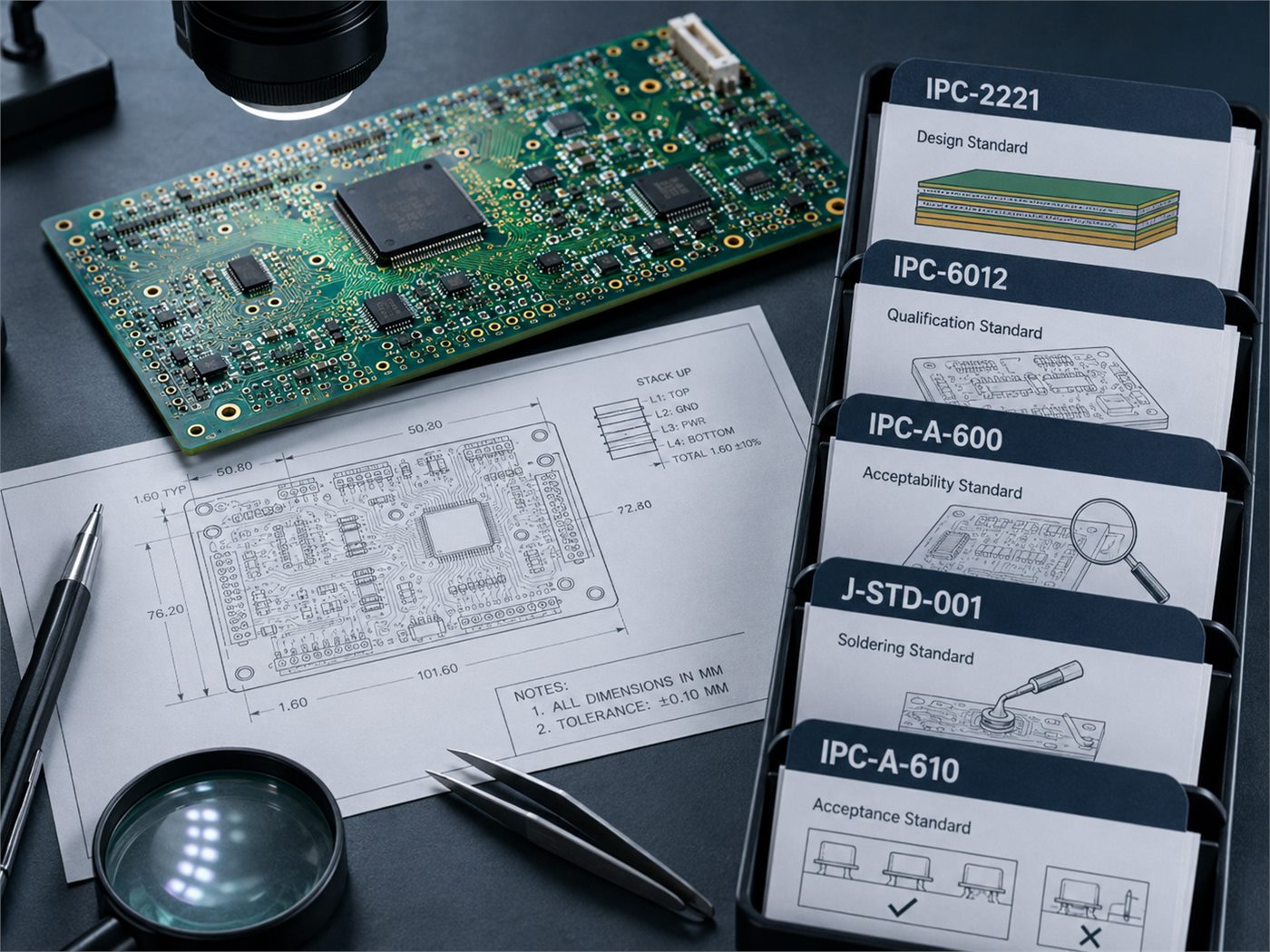
Common quality references include IPC-A-610 for electronic assembly acceptability and IPC J-STD-001 for soldered assembly requirements. RoHS, REACH, UL, and customer-specific standards may also apply depending on the product and target market.
Common IC Board Component Failures
Component failures often come from electrical overstress, heat, poor soldering, wrong part selection, ESD, moisture, mechanical stress, or contamination.
Failure
Common Cause
Prevention
Burned IC
Overvoltage or reverse polarity
Add protection circuit and verify power design
Cracked MLCC
PCB bending or thermal shock
Improve placement and use proper package size
BGA open joint
Warpage or poor reflow
Control profile and use X-ray inspection
MOSFET overheating
Poor copper area or wrong rating
Check RDS(on), thermal vias, and heat path
Connector failure
Vibration or weak plating
Choose correct locking style and plating
Corrosion
Flux residue or moisture
Improve cleaning, coating, and storage
Wrong component
BOM error or feeder mistake
Use barcode control and first article inspection
A failed part is often only the visible result. The root cause may be in design margin, layout, soldering process, component sourcing, or field environment.
How to Choose an IC Board Assembly Supplier?
A reliable supplier should understand both component sourcing and PCB assembly. The supplier should be able to review Gerber files, BOM, footprints, soldering requirements, test points, package risks, and production feasibility.
For turnkey PCB assembly, the supplier should support SMT, through-hole assembly, AOI, X-ray, functional testing, component procurement, and engineering feedback. For OEM and ODM projects, the supplier should also help with prototype development, batch production, cost optimization, and custom engineering support.
If you are looking for a supplier that can support both engineering review and reliable production, EBest Circuit can help you move from design files to finished IC board assembly with less risk. Our team supports PCB fabrication, component sourcing, SMT assembly, through-hole assembly, functional testing, OEM production, ODM development, prototypes, and batch manufacturing. For more information, welcome to contact us at sales@bestpcbs.com or leave your comments on below.
FAQs About IC Board Components
What are the most common IC board components? The most common IC board components include ICs, resistors, capacitors, diodes, transistors, inductors, connectors, crystals, switches, relays, LEDs, and protection devices. Each part supports a different circuit function, such as control, filtering, power regulation, protection, or signal transfer.
Is an IC board the same as a PCB? Not exactly. A PCB is the bare printed circuit board. An IC board usually refers to a PCB assembled with integrated circuits and other components. After assembly, it is often called a PCBA.
What does an IC do on a circuit board? An IC performs a defined electronic function. It may process data, control power, store information, amplify signals, drive loads, or manage communication. Supporting components help the IC operate safely and reliably.
Why are capacitors placed close to ICs? Capacitors placed near IC power pins reduce noise and stabilize voltage. These parts are called decoupling capacitors. Poor placement can cause resets, unstable signals, or power rail noise.
How do I identify components on an IC board? You can identify parts by reference designators, package shape, markings, and circuit position. Common markings include R for resistors, C for capacitors, D for diodes, U for ICs, and J or CN for connectors.
What causes IC board components to fail? Common causes include overvoltage, overheating, ESD, wrong polarity, poor soldering, moisture, vibration, contamination, counterfeit parts, and weak design margin. Failure analysis should check both the part and the surrounding circuit.
Can IC board components be replaced? Many parts can be replaced, but fine-pitch ICs, QFNs, and BGAs need professional rework tools. The replacement part must match the correct package, orientation, electrical rating, and soldering requirement.
What is the difference between SMT and through-hole components? SMT parts are mounted on the PCB surface and are suitable for compact automated assembly. Through-hole parts use leads inserted into holes and provide stronger mechanical support, especially for connectors and large components.
Why is component sourcing important? Good sourcing reduces the risk of counterfeit parts, poor solderability, wrong date codes, unstable quality, and production delays. Critical components should come from approved and traceable channels.
What files are needed for IC board assembly quotation? A complete quotation package usually includes Gerber files, BOM, pick-and-place file, assembly drawing, quantity, surface finish, test requirements, and quality standards. Turnkey assembly also needs clear sourcing requirements.
How can buyers reduce IC board component cost? Buyers can reduce cost by approving alternative parts, choosing standard packages, avoiding obsolete components, reviewing the BOM early, optimizing the PCB panel, and confirming the required test level before production.
How do I choose a manufacturer for IC board assembly? Choose a manufacturer that can support component sourcing, PCB fabrication, SMT assembly, through-hole assembly, AOI, X-ray, functional testing, and engineering review. For OEM and ODM work, prototype and mass production experience are both important.
Conclusion
IC board components determine circuit function, assembly quality, product reliability, and long-term production stability. A good design should consider component rating, package type, PCB material, thermal path, soldering process, inspection method, and supply-chain risk from the beginning.
For selection, engineers should focus on electrical margin, thermal performance, manufacturability, and test coverage. Buyers should focus on BOM accuracy, sourcing traceability, approved alternatives, cost control, and supplier capability.
If you need IC board assembly, OEM production, ODM development, prototype support, or batch manufacturing, working with a source factory that understands both PCB manufacturing and component assembly can reduce design risk and improve delivery efficiency.
A rigid PCB 5V addressable RGB strip is a straight or shaped FR4 LED module where each RGB pixel can be controlled individually through a digital data signal. It is a better choice than a flexible LED strip when the product needs mechanical stability, predictable solder quality, stronger connector retention, or a custom board shape for an OEM lighting assembly.
The biggest engineering risks are not the RGB effect itself. The real risks are voltage drop, copper width, LED current, data signal integrity, heat, connector rating, and whether the supplier can test every pixel before shipment.
A 5V addressable RGB rigid PCB strip needs both optical design and careful power distribution.
Quick Answer: When Should You Use This Type of LED PCB?
Use a rigid PCB 5V addressable RGB strip when you need individually controlled RGB pixels on a stable board that can be mounted, screwed, snapped, or assembled into a product repeatedly.
Decision Point
Rigid PCB 5V Addressable RGB Strip Fits When
Watch Out For
Buyer or Engineering Note
Product structure
The LED module is fixed inside a housing, display, fixture, machine, or sign.
Do not use rigid PCB where the strip must bend after assembly.
Confirm screw holes, edge clearance, and connector location early.
Control method
Each LED or pixel group needs individual color control.
Some LEDs have strict timing and reset requirements.
Match the controller firmware to the LED IC, such as WS2812B or SK6812.
Power
The system already uses 5V DC or has a reliable 5V regulator.
Long strips can suffer voltage drop and color shift.
Plan power injection pads and wide 5V/GND copper.
Manufacturing
You need repeatable SMT assembly and full pixel testing.
Poor reflow control can damage LEDs or create color inconsistency.
Ask for optical and electrical test records.
Customization
You need custom length, pitch, mounting holes, connectors, or shape.
Small design changes affect panelization and cost.
Provide mechanical drawings together with Gerber and BOM files.
What Makes It Different from a Flexible Addressable LED Strip?
A rigid PCB strip uses a hard board material, commonly FR4, instead of a bendable flexible circuit. This changes mechanical performance, solder joint stability, mounting options, and heat spreading.
Item
Rigid PCB Addressable RGB Strip
Flexible Addressable RGB Strip
Practical Difference
Mechanical behavior
Stable and non-bending
Bendable and easy to route around curves
Rigid PCB is better for repeatable mounting and fixture integration.
Assembly stability
Good SMT support and flatness
Can be affected by flex handling and adhesive backing
Rigid board is easier to fixture during production testing.
Connector strength
Better for terminal blocks, board-to-wire, or board-to-board connectors
Often uses solder pads or light-duty connectors
Important for OEM products with repeated assembly.
Thermal path
Can use wider copper and mounting contact to a housing
Depends heavily on flex copper and installation surface
Rigid PCB may be easier to cool in enclosed products.
Custom shape
Can be routed, slotted, drilled, or made into modular sections
Better for long continuous curved paths
Choose based on mechanical design, not only LED type.
Common Related LED and PCB Options
Most buyers comparing this product also compare LED IC type, voltage, board material, pixel density, and connector style. The table below helps avoid mixing terms that sound similar but lead to different designs.
Item / Related Term
What It Means
When It Applies
How It Differs
Buyer or Engineering Note
WS2812B RGB strip
Common 5V addressable RGB LED with integrated control circuit
Decorative lighting, indicators, small displays, OEM modules
One data line controls chained pixels
Check timing, data direction, and maximum current during full white.
SK6812 RGB or RGBW strip
Addressable LED family often used for RGB or RGBW lighting
Projects needing RGBW or alternate package options
Firmware settings may differ from WS2812B
Confirm RGB/RGBW order before production.
5V addressable LED strip
Low-voltage strip where pixels are digitally controlled
Short runs, controller-driven effects, individual pixel control
Higher current than 12V or 24V for the same power
Plan power injection for long or high-density layouts.
12V addressable strip
Higher-voltage addressable lighting option
Longer wiring runs or lower current distribution
May use grouped pixels or different driver design
Check whether every LED is individually addressable.
Specify thickness, copper weight, solder mask color, and mounting holes.
Aluminum LED PCB
Metal-core PCB for better thermal performance
Higher power or heat-sensitive lighting modules
Different cost, drilling, insulation, and routing constraints
Use when heat is a stronger concern than routing complexity.
How a 5V Addressable RGB Strip Works
Each addressable RGB LED package includes RGB emitters and a small control circuit, so the controller sends serial data through the strip and each pixel passes the remaining data to the next LED.
With common LED families such as WS2812B and SK6812, the board usually has 5V, GND, data input, and data output paths. The PCB designer must route power rails wide enough for current, maintain clean data routing, place input/output pads clearly, and protect the strip from assembly mistakes.
Wide 5V and GND copper paths are critical because addressable RGB LEDs can draw high current at full brightness.
Power Design: 5V, Current, and Voltage Drop
Power distribution is the most common failure point in 5V addressable RGB strips because low voltage means higher current for the same wattage.
When all pixels show bright white, every RGB channel can draw current. The far end of a long strip may receive less than the input voltage because copper traces, wires, connectors, and solder joints all add resistance. The visible symptoms are dim LEDs, yellowish white, random flicker, reset behavior, or color mismatch between the near and far ends.
Power Design Checklist
Estimate worst-case current: Calculate full-white current from LED datasheets and safety margin.
Use wide 5V and GND rails: Do not route high-current power as thin signal traces.
Add power injection pads: Long strips should have feed points at intervals, not only one input end.
Check connector rating: Connector current rating must match the real strip load.
Measure voltage at the far end: Test under full-brightness patterns, not only colorful demo effects.
Consider copper weight: Higher current may require wider copper, thicker copper, or shorter segments.
Plan heat path: High brightness in an enclosed product needs thermal evaluation.
PCB Design Requirements for Rigid RGB Strips
The PCB layout should be designed around current flow, LED placement accuracy, optical alignment, and assembly test access.
Design Area
Recommended Engineering Focus
Common Mistake
Supplier Check
LED pitch
Keep pitch consistent for visual uniformity
Changing pitch without updating optics or housing
Ask for SMT placement tolerance and first-article photos.
Copper rails
Use wide 5V and GND routing, with enough copper near connectors
Thin rails causing voltage drop and heat
Review Gerber copper width before production.
Data line
Route cleanly from DIN to DOUT, with clear direction marking
Confusing input and output pads during assembly
Specify data direction in silkscreen and test fixture.
Test pads
Add accessible 5V, GND, DIN, DOUT, and segment test pads
No way to isolate a failing LED chain
Ask whether the factory can test every strip with a fixture.
Panelization
Use rails, tabs, V-cut, or routing based on strip shape
Weak tabs breaking LED solder joints during depaneling
Review depaneling method with the PCB supplier.
Mounting holes
Keep copper and LEDs away from screw stress zones
Cracking solder joints near mounting points
Confirm mechanical drawing with tolerances.
LED Selection: WS2812B, SK6812, RGB, or RGBW
The LED IC should be selected by controller compatibility, color requirement, package size, supply voltage, brightness, white channel needs, and availability.
WS2812B-style LEDs are widely used for 5V RGB addressable lighting, while SK6812 variants are common when RGBW or alternate packages are needed. The final choice should be verified against the controller firmware, color order, timing requirements, and supply chain stability. For production, do not substitute LED models without approval because the same footprint can still behave differently in color order, timing, reset behavior, brightness, or thermal performance.
Manufacturing and Assembly Concerns
Rigid addressable RGB strips look simple, but production quality depends on LED handling, solder paste control, reflow profile, depaneling, and full-function testing.
Moisture sensitivity: LED packages should be stored and baked according to supplier requirements when needed.
Polarity and orientation: RGB LEDs and data direction must be controlled by BOM, silkscreen, and AOI settings.
Solder paste volume: Too much paste can create bridging; too little can reduce mechanical strength.
Reflow profile: Overheating may damage LEDs or create color inconsistency.
Depaneling stress: Long narrow boards need careful support to avoid bending and solder joint cracks.
Functional testing: Every strip should be tested for red, green, blue, white, data-through, and current behavior.
Production testing should verify color channels, data chain continuity, current, and visual consistency.
Testing Plan for Production Orders
A reliable supplier should test addressable RGB strips with both electrical and visual methods, not only a quick power-on check.
Test Item
Purpose
What to Look For
Why Buyers Should Care
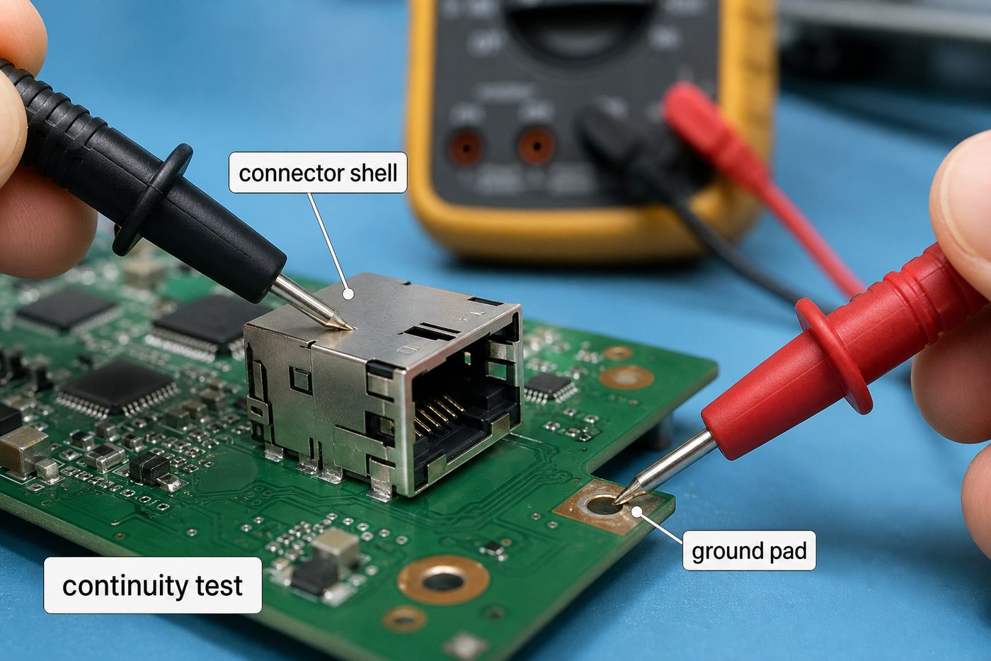
Continuity test
Check 5V, GND, and signal paths
Open circuits, shorts, reversed connections
Prevents dead strips before LED test.
RGB channel test
Light red, green, and blue separately
Wrong color order, missing channel, damaged LED
Finds assembly and LED defects early.
Full-white current test
Measure worst-case current draw
Overcurrent, weak power rails, voltage drop
Important for power supply and connector selection.
Data-through test
Confirm the signal passes from pixel to pixel
Broken chain after one LED, bad solder joint, wrong orientation
One bad pixel can disable the downstream section.
Visual uniformity check
Review brightness and color consistency
Dim pixels, color shift, uneven soldering or LED bins
Critical for visible lighting products.
Procurement Checklist Before Ordering
Buyers should send both electrical and mechanical requirements, because a rigid PCB LED strip is part PCB, part lighting product, and part assembly module.
Target LED IC or accepted alternatives, such as WS2812B, SK6812, RGB, or RGBW.
Operating voltage, maximum current, expected brightness level, and duty cycle.
Board length, width, thickness, mounting holes, slots, and outline tolerance.
LED pitch, LED count, color order, and data direction.
Copper weight, surface finish, solder mask color, and silkscreen requirements.
Connector type, cable length, wire gauge, and current rating.
Testing method, acceptance criteria, packaging, and labeling requirements.
Whether the strip must pass product-level requirements such as EMC, flammability, or safety review.
Common Failure Modes
Most failures come from power distribution, poor LED soldering, data chain interruption, heat, or mechanical stress.
Symptom
Likely Cause
Engineering Fix
Production Check
End pixels look dim or yellow
Voltage drop along 5V/GND rails
Wider copper, shorter segments, or power injection
Measure far-end voltage at full white.
Pixels flicker randomly
Weak data signal, poor grounding, or unstable power
Improve ground reference, routing, controller level, and power filtering
Run dynamic color sequence tests.
All pixels after one LED fail
Broken data output or wrong LED orientation
Check LED direction, solder joints, and DOUT path
Use fixture test to locate chain break.
Connector gets hot
Current exceeds connector or wire rating
Use higher-rated connector or multiple feeds
Thermal check during full-brightness burn-in.
Board cracks near mounting hole
Mechanical stress or poor hole clearance
Add clearance, support, or change mounting structure
Review mechanical drawing and screw torque.
FAQ
What is a rigid PCB 5V addressable RGB strip?
It is a non-flexible LED PCB module with individually controllable RGB pixels, usually powered by 5V DC and controlled through a digital data line. It is commonly used in OEM lighting modules, displays, indicators, and custom electronics.
Why choose rigid PCB instead of flexible LED strip?
Rigid PCB is better when the strip must mount flat, hold connectors firmly, maintain LED position, or pass repeatable assembly testing. Flexible strip is better when the installation needs bending around curves.
Is 5V enough for addressable RGB LEDs?
Yes, many addressable RGB LEDs are designed for 5V operation. The key is current planning. Long strips and high-density layouts need wide copper, suitable connectors, and often power injection.
How do I avoid voltage drop on a 5V RGB strip?
Use wide 5V and GND copper, keep high-current paths short, add power injection pads, choose connectors with enough current rating, and test the far-end voltage under full-white brightness.
Can every LED be individually controlled?
With common addressable RGB LEDs, each pixel can usually be controlled individually. However, some higher-voltage or cost-reduced products may group LEDs, so buyers should confirm pixel control before ordering.
What LED ICs are commonly used?
WS2812B and SK6812 families are common examples for 5V addressable RGB or RGBW products. The final choice should match the controller, color order, firmware timing, package, brightness, and availability.
Do rigid RGB strips need test pads?
Yes. Test pads for 5V, GND, DIN, DOUT, and segment points make production testing and fault diagnosis much easier, especially when one LED can interrupt the downstream data chain.
What copper weight should I use?
It depends on current, trace width, strip length, board temperature, and allowed voltage drop. For high-current strips, ask the PCB supplier to review copper width and current path before production.
Can a rigid PCB RGB strip be waterproof?
The PCB itself is not automatically waterproof. Waterproofing may require conformal coating, silicone encapsulation, housing design, or sealed connectors. Each method affects heat, repairability, and optical appearance.
What files should I send to a supplier?
Send Gerber files, BOM, pick-and-place file, mechanical drawing, LED specification, connector requirements, testing requirements, target quantity, packaging needs, and any controller compatibility details.
Can the same design use RGBW LEDs?
Possibly, but RGBW LEDs may have different pinout, current, package, firmware settings, color order, and optical requirements. Do not substitute RGBW without redesign review.
What should be tested before mass production?
Test RGB channels, full-white current, data-through continuity, far-end voltage, visual uniformity, connector heating, mounting fit, and controller compatibility before releasing mass production.
Final Recommendation
A rigid PCB 5V addressable RGB strip is a strong choice when you need a stable, custom, individually controlled lighting module for an OEM product. The design should be reviewed as a complete electrical, mechanical, optical, and manufacturing system, not just as a row of LEDs.
If you’re sourcing reliable PCB/PCBA manufacturing, including OEM, ODM, prototyping, mass production, or custom engineering solutions, reach out to our engineering team for technical support and a quote at sales@bestpcbs.com.
High reliability medical PCBA is essential for medical electronics that need stable power, accurate signals, long service life and controlled production records. In medical device projects, a small soldering defect, unstable component source or missing test record may lead to delays, field failures or costly redesign.
Are you worried about unstable medical PCBA quality, hidden BGA defects, unclear component traceability or delayed production approval? These problems often appear during prototype validation, pilot runs or repeat orders, especially when the design, sourcing and assembly process are not controlled together.
EBest Circuit is a China-based source factory providing PCB manufacturing, SMT assembly, component sourcing, testing and traceable production for global medical electronics customers. We support high reliability medical PCBA prototypes, pilot runs and mass production for OEM brands, engineering teams and healthcare device manufacturers.
What Is High Reliability Medical PCBA?
High reliability medical PCBA is a printed circuit board assembly designed and manufactured for medical electronics where stable performance, safe operation and traceable quality are required. It includes PCB fabrication, component sourcing, SMT assembly, inspection, testing and controlled documentation.
Unlike standard PCBA, high reliability medical PCBA focuses on design risk control, solder joint reliability, clean production, component traceability and repeatable testing. It is used in devices where power stability, signal accuracy, connector strength and long-term operation cannot be compromised.
For medical electronics buyers, the value is clear: fewer hidden defects, better batch consistency and easier quality tracking from prototype to mass production.
Why Is High Reliability Critical for Medical Electronics?
High reliability is critical because medical electronics are often used for patient monitoring, diagnosis, therapy control and healthcare data collection. A small PCBA defect may cause unstable readings, power interruption or intermittent device operation.
Patient safety: Poor soldering, unstable power or signal noise can affect device accuracy.
Signal stability: Monitoring and diagnostic devices need clean signal paths and reliable grounding.
Long operating time: Weak solder joints, hidden BGA defects or connector stress may fail after delivery.
Traceability: Clear material and process records make failure analysis faster.
Lower recall risk: Stable production reduces batch problems, after-sales cost and approval delays.
High reliability medical PCBA should be controlled from design review to final packaging, not only checked before shipment.
What Medical Devices Need High Reliability Medical PCBA?
High reliability medical PCBA is used in medical devices that need accurate signals, stable control and dependable long-term operation. These boards may handle sensing, display control, wireless communication, power management or battery charging.
Diagnostic instruments: blood analyzers, test modules, imaging control boards and laboratory equipment.
Wearable healthcare electronics: health patches, portable sensors and rechargeable monitoring devices.
Therapeutic equipment: infusion pumps, rehabilitation devices and electronic control modules.
Medical communication modules: wireless medical IoT boards and data transmission modules.
Handheld medical tools: portable test devices and battery-powered medical electronics.
These devices need stable PCBA quality because failure may affect accuracy, uptime and user confidence.
What Reliability Requirements Matter Most for Medical PCBA?
Medical PCBA reliability depends on approved materials, stable assembly, complete inspection and traceable records. Requirements vary by device function, environment and customer standard.
Quality system control: ISO 13485 project support can be applied when medical-grade documentation is required.
Assembly acceptance: IPC-A-610 Class 2 or Class 3 can be selected by product risk.
Soldering control: IPC J-STD-001 reference helps control solder joint workmanship.
Bare PCB quality: IPC-A-600 and IPC-6012 references help check PCB fabrication quality.
Material compliance: RoHS, REACH and approved BOM control reduce sourcing risk.
Hidden joint inspection: X-ray is used for BGA, QFN, LGA and bottom-terminated parts.
Batch traceability: PCB lot, component lot, solder paste batch and test results should be linked.
Functional verification: ICT, FCT, programming or aging test can be selected by product function.
The real requirement is repeatable process control across prototype, pilot run and repeat orders.
What Design Factors Affect Medical PCBA Reliability?
Medical PCBA reliability starts with design. A strong assembly line cannot fully fix poor heat dissipation, weak grounding, tight clearance or missing test points.
Design factors include:
Stack-up design: affects impedance, EMI control and mechanical stability.
Power layout: affects voltage drop, heat generation and current capacity.
Grounding design: reduces noise and improves signal accuracy.
Thermal paths: copper area, thermal vias and spacing help control heat.
Component spacing: improves soldering quality and rework safety.
Connector position: reduces mechanical stress during use.
Test point access: supports inspection, programming and functional testing.
Good design choices reduce production defects and make high reliability medical PCBA easier to manufacture repeatedly.
How Does DFM Review Reduce Medical PCBA Failure Risk?
DFM review finds fabrication, assembly and testing risks before production starts. This helps prevent avoidable soldering defects, rework, delivery delays and batch instability.
With proper DFM review, customers can reduce redesign, rework, unstable samples and mass production delays.
How Does Component Selection Improve Medical PCBA Reliability?
Component selection affects medical PCBA reliability because poor parts can cause failure even when soldering quality is good. Medical electronics often need stable sourcing, long lifecycle parts and approved substitutes.
Reliable component selection should consider:
Original source: Reduces fake parts, mixed lots and uncontrolled suppliers.
Lifecycle status: Avoids obsolete or end-of-life components.
Electrical margin: Confirms voltage, current, tolerance and temperature rating.
Package reliability: Fine-pitch, BGA and QFN parts need suitable pads and inspection.
Supply stability: Long lead time parts should be reviewed before production.
Approved alternates: Replacement parts should be confirmed before use.
For high reliability medical PCBA, the cheapest component is not always the safest choice. Stable sourcing protects quality, delivery and repeat production.
How Does SMT Assembly Quality Affect Medical PCBA Stability?
SMT assembly quality affects solder joint strength, electrical stability and long-term reliability. Poor paste printing, inaccurate placement or unstable reflow can create hidden defects.
SMT process control includes:
Solder paste printing: Controls paste volume, position and consistency.
SPI inspection: Checks paste height, area and offset before placement.
Component placement: Controls polarity, rotation, package accuracy and pressure.
Reflow profile: Controls heating, soaking, peak temperature and cooling.
First article inspection: Confirms BOM, placement and assembly accuracy.
Stable SMT assembly reduces intermittent failures and batch variation in medical electronics production.
How Are BGA, QFN and Fine-Pitch Components Controlled in Medical PCBA?
BGA, QFN and fine-pitch components require strict control because many solder joints are hidden under the package. Visual inspection alone is not enough.
Control methods include:
Pad design review: Confirms pad size, solder mask opening and via-in-pad risk.
Stencil tuning: Adjusts paste openings for thermal pads and small pitches.
Placement accuracy: Controls nozzle selection, alignment and placement pressure.
Reflow control: Reduces insufficient wetting, voids and solder bridging.
Process feedback: Uses inspection results to adjust stencil, profile or placement settings.
For high reliability medical PCBA, BGA and QFN control directly affects long-term reliability.
How Is Cleanliness Controlled During High Reliability Medical PCBA Production?
Cleanliness control reduces leakage, corrosion and unstable performance. This is especially important for humid environments, low-current circuits, sensor interfaces and high-density medical boards.
Cleanliness control includes:
Material handling: Controls PCB, components, solder paste and storage conditions.
Process control: Reduces excess flux, solder balls, dust and handling contamination.
Cleaning method: Applies cleaning when product risk or customer standard requires it.
Visual inspection: Checks residue, stains, particles and foreign material.
Ionic contamination check: Verifies cleanliness for sensitive boards when required.
Packaging control: Uses ESD bags, moisture protection and clean packing.
Clean production helps medical electronics maintain stable signals and low leakage risk.
How Is Traceability Managed for Medical PCBA Manufacturing?
Traceability connects every medical PCBA batch with its materials, process records, inspection results and test data. When a problem appears, traceability helps identify the affected lot and speed up root cause analysis.
Traceability can include:
PCB lot number: Board supplier, date, panel batch and specification.
Component lot data: Part number, supplier, date code and quantity.
Solder paste record: Paste type, batch, storage and usage time.
Production record: SMT line, operator, date and reflow profile.
Inspection record: SPI, AOI, X-ray and manual inspection results.
Test record: Programming, ICT, FCT, aging test and final QA result.
Shipment record: Labels, quantity, packaging and delivery information.
For medical device buyers, traceability improves batch containment and repeat-order stability.
How Does Our Quality Inspection Process Work for High Reliability Medical PCBA?
Our quality inspection process follows the production flow. The goal is to detect defects early, confirm assembly stability and provide clear records before shipment.
Step 1: Incoming material inspection. We check bare PCB quality, component part numbers, package types, quantity, date codes, solder paste condition and production documents. This prevents wrong materials, mixed lots and sourcing errors.
Step 2: First article inspection. Before batch assembly continues, we verify placement, polarity, package, reference designator, solder result and BOM matching. This confirms the SMT program, stencil and setup.
Step 3: Solder paste inspection. SPI checks paste height, area, volume and offset after printing. This reduces solder bridges, insufficient solder and weak joints before placement.
Step 4: SMT assembly inspection. After reflow, AOI checks missing parts, wrong parts, polarity errors, solder bridges and visible solder defects. Manual inspection checks connectors, labels, THT parts and appearance.
Step 5: Hidden joint inspection. For BGA, QFN, LGA and bottom-terminated parts, X-ray checks hidden solder joints, voids, shorts, opens and ball shift.
Step 6: Electrical and functional testing. We check shorts, opens, voltage rails, programming status, communication signals and product functions according to the test plan.
Step 7: Final QA and packaging. Before shipment, we verify quantity, labels, records, test results and packaging. ESD, moisture and shock protection are applied as required.
What Testing Methods Are Used to Verify Medical PCBA Reliability?
Testing confirms whether the medical PCBA meets electrical and functional requirements. Test coverage should match circuit complexity and product risk.
Common testing methods include:
Electrical testing: Checks opens, shorts and basic continuity.
ICT: Tests components, solder joints and circuit nodes when test points are available.
Functional testing: Verifies power, signals, communication and product functions.
Programming: Loads firmware and checks boot or communication status.
Aging test: Runs the PCBA for a defined time to find early failures.
Thermal check: Reviews heat points under working conditions.
Custom fixture testing: Simulates product operation for repeatable production testing.
For high reliability medical PCBA, functional testing should match real operating conditions as closely as possible.
How Do We Support Medical PCBA Prototype and Mass Production?
We support high reliability medical PCBA from prototype to mass production by keeping engineering review, material control and inspection records connected across each stage.
For prototypes, we focus on DFM feedback, BOM review, fast assembly, sample inspection and functional verification. This helps engineers find design or sourcing problems before pilot production.
For mass production, we focus on approved materials, fixed process parameters, test fixtures, traceability and packaging consistency. This helps reduce order-to-order variation.
Customers can use prototype results to improve the design, then move toward batch production with fewer changes, fewer delays and better reliability control.
What High Reliability Medical PCBA Services Can EBest Provide?
EBest Circuit provides high reliability medical PCBA services from PCB fabrication to SMT assembly, component sourcing, testing and box assembly. Customers can manage more work through one China-based source factory.
Our services include:
PCB fabrication: FR4 PCB, multilayer PCB, metal-based PCB, ceramic PCB, flexible PCB, rigid-flex PCB and high frequency PCB.
Prototype PCB assembly: Sample builds for validation, engineering tests and pilot production.
Quick turn PCB assembly: Short lead time support for urgent projects.
Full turnkey PCB assembly: PCB production, sourcing, assembly, inspection, testing and packaging.
BGA assembly service: Support for BGA, QFN, QFP and fine-pitch components.
Through-hole and mixed assembly: SMT, THT and mixed assembly for connectors, terminals and control boards.
Flex PCB assembly: Support for wearable devices, sensors and compact modules.
Ceramic PCB assembly: Suitable for heat-resistant or stable material requirements.
Box assembly: Enclosure assembly, labeling, testing and delivery preparation.
Component sourcing: Supply support for SMD parts, BGA, QFN, QFP and other components.
These services help customers reduce supplier handoffs, unclear responsibility and production risk.
Case Study: High Reliability Medical PCBA for a Patient Monitoring Device
Project background: A customer needed a high reliability medical PCBA for a patient monitoring device. The board included sensor input circuits, a microcontroller, power management, display connectors and a wireless module.
Project requirements: The project required stable sensor signals, reliable BGA and QFN soldering, safe battery power management, repeatable functional testing and traceable production records.
Our solution: EBest Circuit reviewed the Gerber files, BOM, test points, polarity marks and fine-pitch layout before production. We checked pad design, stencil openings and component spacing to reduce soldering risk.
During production, SPI checked solder paste, AOI checked placement, and X-ray inspected hidden BGA and QFN solder joints. Functional testing covered power rails, display connection, communication interface and sensor input.
Output result: The prototype passed visual inspection, X-ray inspection and functional testing. The customer received traceable records and used the sample result to support pilot production.
The project helped reduce assembly risk, improve test clarity and create a stable path from prototype validation to batch delivery.
Why Choose EBest as Your High Reliability Medical PCBA Manufacturer?
Choosing EBest Circuit helps medical electronics buyers reduce supplier management, improve assembly stability and move faster from prototype to production. Customers can handle PCB fabrication, component sourcing, assembly, testing and box assembly through one China-based manufacturer.
Lower coordination cost: PCB fabrication, component supply, SMT assembly, testing and box assembly can be handled together.
Stable production support: SMT, THT and mixed assembly support different medical electronics designs.
Dense board capability: EBest can handle 01005 minimum SMD components and 0.25mm minimum BGA pitch.
Flexible order support: Prototype, low-volume production and repeat orders can be arranged by project stage.
Fast project response: PCBA lead time can be 1–5 days, depending on file readiness, BOM status and complexity.
Flexible component handling: Reels, cut tape, tubes, trays and loose parts can be managed.
Quality confidence: EBest supports ISO 9001:2015, ISO 13485:2016, IATF 16949, AS9100D, UL, RoHS and REACH.
Delivery support: Box assembly, inspection, labeling, packaging and export preparation reduce final delivery problems.
FAQs About High Reliability Medical PCB Assembly
Q1: What files should I send before requesting a quotation? A1: Send Gerber files, BOM, pick-and-place file, assembly drawing, PCB specification and test requirements. If the project includes firmware, coating, labels or box assembly, share those files early.
Q2: What should I check before approving the first sample? A2: Check placement, polarity, solder quality, connector fit, firmware version, functional test result, label accuracy and packaging method. For BGA or QFN designs, review X-ray results.
Q3: How can buyers reduce risk before repeat orders? A3: Lock the approved Gerber files, BOM revision, firmware version, test method, inspection standard and packaging requirement before repeat production.
Q4: What happens if a component becomes unavailable during production? A4: The safest method is to review approved alternates before replacement. The substitute should match package, rating, tolerance, temperature range and reliability needs.
Q5: Should firmware programming be included in medical PCBA production? A5: Firmware programming should be included when the board needs software to boot, communicate or complete testing. The programming file, version and test method should be confirmed before production.
Q6: What affects the final medical PCBA cost most? A6: Cost is affected by PCB complexity, component availability, assembly density, BGA quantity, testing requirements, coating, box assembly and packaging method. DFM review, BOM review and test planning help control cost early.
Q7: How long does high reliability medical PCBA production usually take? A7: Lead time depends on PCB complexity, BOM availability, SMT density, BGA inspection, testing and packaging needs.
Q8: Can high reliability medical PCBA support low-volume orders? A8: Yes. Low-volume production is suitable for engineering samples, validation, pilot runs and early market testing.
Q9: When is conformal coating needed for medical PCBA? A9: Conformal coating is useful when the board may face humidity, dust, condensation or chemical exposure. Connectors, sensors, test points and switches may need masking.
Q10: Can a China-based source factory support global medical electronics buyers? A10: Yes. A China-based source factory can support global buyers with PCB fabrication, PCBA production, testing, packaging and export delivery.
Conclusion
High reliability medical PCBA requires controlled PCB fabrication, stable component sourcing, precise SMT and THT assembly, BGA inspection, functional testing, traceable records and reliable packaging. These controls help reduce field failure, approval delays and repeat-order variation.
If you are developing patient monitoring devices, diagnostic instruments, wearable healthcare electronics, medical communication modules or custom medical control boards, EBest Circuit can support your project from prototype to batch production. Send your Gerber files, BOM, assembly drawings and test requirements to us today for engineering review and quotation: sales@bestpcbs.com.
A DMOS transistor is a special type of MOSFET designed for power control, fast switching, and higher voltage operation. If a small signal transistor is like a small tap controlling a thin stream of water, a DMOS transistor is more like a strong electronic valve. It allows a small control signal to manage a much larger current in a circuit.
DMOS stands for double-diffused metal-oxide-semiconductor. The name sounds technical, but the basic idea is not difficult. A DMOS transistor uses a special internal structure to create a short channel and a voltage-supporting drift region. The short channel helps the transistor switch quickly. The drift region helps the device withstand higher voltage when it is turned off.
This makes DMOS transistors useful in power supplies, motor drivers, automotive electronics, LED drivers, battery protection circuits, industrial control boards, and RF power circuits. For PCB and PCBA projects, understanding DMOS transistors is helpful because these components often sit near high-current paths, switching nodes, heat-generating loads, and power-control areas.
What Is a DMOS Transistor?
A DMOS transistor is a MOSFET built with a double-diffused structure. In plain language, it is a voltage-controlled transistor that allows current to flow between drain and source when the gate voltage is applied correctly.
A basic MOSFET has three important terminals:
Terminal
Simple Meaning
What It Does
Gate
Control pin
Turns the transistor on or off
Drain
Output current path
Current usually enters or leaves here, depending on circuit type
Source
Reference current path
Often connected to ground or a supply rail
Body / Substrate
Internal semiconductor base
Supports the device structure
In a MOSFET, the gate is insulated from the current path by a thin oxide layer. When voltage is applied to the gate, it creates an electric field. This electric field forms a channel between source and drain, allowing current to flow.
A DMOS transistor follows the same basic MOSFET idea, but its internal structure is optimized for power. The “double-diffused” part helps define a short channel and a drift region. The short channel supports fast switching, while the drift region helps the transistor block higher voltage when it is turned off.
The easiest definition is this:
A DMOS transistor is a power-oriented MOSFET structure that uses double diffusion to achieve fast switching, high voltage capability, and efficient current control.
What Does a DMOS Transistor Do?
A DMOS transistor mainly works as an electronic switch. It can turn current on and off quickly without needing much input power at the gate.
Think of a microcontroller on a PCB. The microcontroller pin may only provide a small control signal. It cannot directly drive a motor, solenoid, relay, heater, or high-power LED. A DMOS transistor can sit between the control signal and the load. The control signal tells the gate what to do, and the DMOS transistor handles the heavier current.
In real circuits, a DMOS transistor can:
Function
Easy Explanation
Common Example
Switch current
Turns a load on or off
Motor driver, relay driver
Control power
Helps regulate voltage or current
DC-DC converter
Drive loads
Handles current for external parts
LED module, solenoid
Protect circuits
Used in power management and protection paths
Battery protection, load switch
Amplify RF power
Used in certain RF power stages
ISM, broadcast, communication equipment
The key point is simple:
A DMOS transistor lets a low-power control signal manage a higher-power circuit.
This is why it is common in power electronics and embedded control systems.
How Does a DMOS Transistor Work?
A DMOS transistor works by using voltage at the gate to control the current path between drain and source.
When the gate voltage is too low, the transistor is off. The path between drain and source is blocked, so current cannot flow through the main channel. When the gate voltage rises above the required level, a channel forms near the surface of the semiconductor. This channel allows current to pass.
You can imagine the gate as a door handle. The drain and source are like two rooms. Without the correct gate voltage, the door stays closed. When the gate voltage is high enough, the door opens and current can move through.
For an N-channel DMOS transistor, which is very common in power circuits:
A positive gate-to-source voltage is applied.
An electric field forms under the gate oxide.
A conductive channel appears.
Current flows between drain and source.
When the gate voltage is removed, the channel disappears.
This is different from a bipolar transistor, such as an NPN transistor. A BJT needs base current to stay on. A MOSFET, including DMOS, is controlled mainly by voltage.
This difference matters in switching circuits. Because the gate does not need continuous drive current in the same way a BJT base does, DMOS transistors can be easier to drive. They are also useful in high-frequency switching because MOSFETs avoid some of the storage-delay problems found in bipolar devices.
DMOS Transistor Structure: What Makes It Different?
The structure is the main reason a DMOS transistor is useful. A normal MOSFET can switch signals, but a DMOS transistor is built to manage power more effectively.
The most important parts inside a DMOS transistor are:
Structure Part
Simple Role
Gate oxide
Insulates the gate and allows electric-field control
Gate electrode
Receives the control voltage
Source region
Provides one side of the current path
Body region
Helps form the channel
Drift region
Supports high voltage when the device is off
Drain region
Provides the other side of the current path
The drift region is especially important. In a high-voltage transistor, the device must survive voltage stress when it is off. The drift region spreads the electric field and helps prevent breakdown.
This creates one of the classic power MOSFET trade-offs:
Higher breakdown voltage usually needs a stronger drift region, but that can increase resistance. Lower resistance improves efficiency, but the device still needs enough voltage strength.
This is why datasheets matter. Two DMOS transistors may look similar from the outside, but their internal structures can be tuned for different voltage, current, switching speed, and thermal behavior.
What Are the Main Characteristics of a DMOS Transistor?
When engineers choose a DMOS transistor, they do not only look at the package size. They check electrical and thermal parameters to make sure the device can work safely in the real circuit.
Breakdown voltage: This tells you how much voltage the transistor can block when it is off. If the circuit voltage is higher than the transistor can handle, the device may fail. A 12V system, for example, should not automatically use a 12V-rated transistor. Designers usually leave margin for spikes, surges, and switching noise.
On-resistance: On-resistance is often shown as RDS(on). It tells you how much resistance exists between drain and source when the transistor is fully on. Lower RDS(on) usually means less heat and better efficiency. In power circuits, this is one of the most important selection points.
Gate threshold voltage: Gate threshold voltage tells you when the transistor just begins to turn on. It does not mean the transistor is fully on. This is a common beginner mistake. For switching applications, you should check RDS(on) at the actual gate voltage used in your circuit.
Switching speed: DMOS transistors can switch quickly. This makes them useful in DC-DC converters, power supplies, and motor control. However, fast switching also makes PCB layout more important. Poor layout can cause ringing, EMI, and heat concentration.
Capacitance and gate charge: The gate behaves partly like a small capacitor. To switch the transistor on and off, the driver must charge and discharge this gate. Higher gate charge can make switching slower or require a stronger driver.
Thermal performance: A DMOS transistor may handle high current on paper, but real performance depends on heat removal. PCB copper area, thermal vias, package type, airflow, and ambient temperature all affect reliability.
Where Are DMOS Power Transistors Used?
DMOS power transistors are used wherever circuits need efficient switching, power control, or high-speed current handling.
Common applications include:
Application
Why DMOS Is Useful
Switching power supplies
Fast switching and efficient current control
DC-DC converters
Helps step voltage up or down efficiently
Motor drivers
Controls current to motors
Automotive modules
Handles loads in body, lighting, and power systems
LED drivers
Controls current for high-power LEDs
Industrial control boards
Drives relays, valves, solenoids, and actuators
Battery protection circuits
Switches charging and discharging paths
RF power circuits
Supports certain high-frequency power applications
In RF applications, DMOS and LDMOS devices can be used in industrial, scientific, medical, broadcast, avionics, radar, telecom, and satellite communication equipment.
For PCB and PCBA projects, DMOS transistors are often found near power inputs, inductors, transformers, motors, connectors, and heat-generating loads. If you see a power device connected to a large copper area, a heat sink, or a switching node, there is a good chance it is handling serious current-control work.
Lateral DMOS Transistor vs Vertical DMOS Transistor: What Is the Difference?
DMOS transistors can be built in different layouts. The two important terms are lateral and vertical.
A lateral DMOS transistor allows current to flow mostly along the surface of the chip. The source, gate, and drain are usually arranged on the top side. This structure is useful for integrated circuits and certain RF applications.
A vertical DMOS transistor allows current to flow vertically through the chip. The source and gate are often on the top side, while the drain is on the backside. This structure is common in discrete power MOSFETs because it supports higher voltage and current.
Here is the simple comparison:
Type
Current Flow
Common Use
Main Advantage
Lateral DMOS / LDMOS
Mostly horizontal
ICs, RF devices, integrated power circuits
Easier integration, good RF behavior
Vertical DMOS
Vertical through the die
Discrete power MOSFETs
Better for higher current and voltage
For a beginner, the easiest way to remember it is this:
Lateral devices are easier to integrate. Vertical devices are often better for handling larger power.
DMOS Transistor vs MOSFET vs CMOS vs NPN Transistor
These terms are often mixed together, so it helps to separate them clearly.
A MOSFET is a general type of transistor controlled by gate voltage. A DMOS transistor is a special MOSFET structure designed for power use. CMOS is not one transistor. It is a circuit technology that uses complementary MOSFETs, usually NMOS and PMOS, to build digital circuits. An NPN transistor is a type of bipolar transistor controlled by base current.
Term
What It Is
Controlled By
Typical Use
MOSFET
A field-effect transistor
Gate voltage
Switching, power control, signal circuits
DMOS transistor
A power MOSFET structure
Gate voltage
Power switching, high-voltage circuits
CMOS
A circuit technology using MOSFET pairs
Logic signals
CPUs, memory, sensors, digital ICs
NPN transistor
A bipolar junction transistor
Base current
Signal switching, amplification
The relationship is simple:
DMOS is a type of MOSFET structure. CMOS is a circuit technology built with MOSFETs. NPN is a different transistor family.
This distinction matters when reading datasheets or discussing PCB design. If someone says “MOSFET,” they may be speaking broadly. If someone says “DMOS,” they are usually talking about a power-oriented MOSFET structure. If someone says “CMOS,” they are usually talking about logic IC technology, not a single discrete transistor.
DMOS Transistor Circuit, Schematic, and Symbol: What Should Engineers Know?
In a schematic, a DMOS transistor usually looks similar to a MOSFET symbol. The symbol shows gate, drain, and source. Some symbols also show the body diode, which is important in power circuits.
The body diode is not an optional external diode. It is part of the MOSFET structure. In some circuits, it helps provide a current path. In other circuits, it may create unwanted conduction if the design is wrong.
A common DMOS transistor circuit is a low-side switch.
In this circuit:
The load connects to the positive supply.
The DMOS transistor sits between the load and ground.
The gate receives a control signal.
When the gate turns on, current flows through the load.
When the gate turns off, current stops.
This setup is common for LEDs, relays, fans, small motors, and solenoids.
Another common design is a high-side switch. In this case, the transistor sits between the power supply and the load. High-side switching is useful when the load must stay connected to ground, but the gate drive is usually more complex.
For PCB layout, the schematic is only half the story. A good DMOS circuit also needs careful copper design. High-current paths should be short and wide. Switching loops should be compact. Gate traces should avoid noise. Thermal vias and copper pours may be needed for heat spreading.
In power circuits, a poor layout can make a good transistor behave badly.
How to Choose the Right DMOS Transistor for a Circuit
Choosing a DMOS transistor is not about picking the part with the highest current rating. Datasheet current ratings are often measured under ideal conditions. Real PCB conditions are different.
Check voltage rating: Choose a drain-source voltage rating higher than your maximum circuit voltage. Add margin for spikes and transients. For example, a 24V system may need a 40V, 60V, or higher-rated part, depending on the environment.
Check current rating: Look at both continuous current and pulse current. Then check whether the PCB and package can actually remove the heat.
Check RDS(on): Lower RDS(on) reduces conduction loss. This is important when the transistor stays on for long periods or carries high current.
Check gate drive voltage: Make sure your control circuit can fully turn the transistor on. A 5V microcontroller may not fully drive every power transistor. A 3.3V microcontroller needs even more attention.
Check switching requirements: For high-frequency switching, look at gate charge, input capacitance, output capacitance, and reverse transfer capacitance. These values affect switching loss and driver selection.
Check thermal path: Look at package thermal resistance, PCB copper area, airflow, and expected ambient temperature. Heat is one of the most common reasons power devices fail.
Check application conditions: Motor loads, inductors, relays, and solenoids can create voltage spikes. The design may need flyback diodes, TVS diodes, snubbers, or proper gate protection.
A good rule is this:
Do not select a DMOS transistor only by voltage and current. Select it by voltage, current, resistance, gate drive, switching speed, thermal design, and load behavior.
Common Mistakes When Using DMOS Transistors
Many DMOS transistor problems come from simple design mistakes. The device itself may be good, but the circuit around it may not support it properly.
Mistake 1: Confusing threshold voltage with full turn-on voltage
The threshold voltage only means the transistor starts to conduct a tiny current. It does not mean it is ready to carry the full load current.
Always check RDS(on) at your actual gate voltage.
Mistake 2: Ignoring heat
A transistor with low resistance still produces heat. If the PCB has poor copper area or weak thermal design, the device may overheat.
Mistake 3: Using long switching loops
Long current loops increase inductance. This can cause voltage spikes, ringing, EMI, and unstable behavior.
Mistake 4: Driving the gate too slowly
A slow gate signal keeps the transistor in its transition region for too long. During this time, voltage and current overlap, creating extra switching loss.
Mistake 5: Forgetting the load type
Inductive loads behave differently from resistive loads. Motors, coils, relays, and transformers can produce high voltage spikes when current changes quickly.
Mistake 6: Not reading the safe operating area
The safe operating area, or SOA, shows what voltage and current combinations the device can survive for a certain time. This matters in linear operation, startup, fault conditions, and pulse loads.
Good engineering is not only about choosing a strong transistor. It is about making sure the whole circuit gives that transistor a safe working environment.
FAQs About DMOS Transistor
Q1: Is a DMOS transistor the same as a MOSFET?
A DMOS transistor is a type of MOSFET structure. All DMOS transistors are MOSFET-based, but not all MOSFETs are DMOS. DMOS is usually used when the device is designed for power handling.
Q2: Why is it called double-diffused?
It is called double-diffused because two diffusion steps are used to form important internal regions of the transistor. These diffusions help define the channel length and support the power structure.
Q3: Can a DMOS transistor be used as a switch?
Yes. Switching is one of its most common uses. It can control motors, LEDs, relays, solenoids, and power conversion circuits.
Q4: What is the main advantage of a DMOS transistor?
The main advantage is efficient power switching. It can handle useful voltage and current while being controlled by gate voltage.
Q5: What is the difference between DMOS and LDMOS?
DMOS is a broader double-diffused MOS structure. LDMOS means laterally diffused MOS and is often used in RF and integrated power applications. LDMOS current flow is mainly lateral, while many power DMOS devices have strong vertical current flow.
Q6: Is DMOS better than an NPN transistor?
It depends on the circuit. For many power switching tasks, DMOS can be easier to drive and more efficient. For some analog or low-cost signal circuits, an NPN transistor may still be suitable.
Q7: What does RDS(on) mean in a DMOS transistor?
RDS(on) is the resistance between drain and source when the transistor is on. Lower RDS(on) usually means less heat and better efficiency.
Q8: Why does PCB layout matter for DMOS transistors?
Because DMOS transistors often switch high current quickly. Poor layout can create heat, noise, voltage spikes, and EMI. Good copper design and short current paths improve reliability.
All in all, a DMOS transistor may sound difficult at first, but its basic job is easy to understand. It is a power-focused MOSFET structure that uses gate voltage to control current. Its double-diffused design helps create a short channel, while its drift region supports higher voltage. This combination makes it useful in switching power supplies, automotive electronics, motor drivers, LED drivers, RF circuits, and industrial control systems.
For PCB and PCBA projects, the transistor itself is only one part of the design. The board must also support current flow, heat dissipation, switching stability, and long-term reliability. At Best Technology, we support customers with PCB manufacturing and assembly for power electronics, automotive modules, industrial control boards, LED applications, and other electronic products. If your project uses DMOS transistors, MOSFETs, power ICs, or high-current circuits, our engineering team can help review manufacturability, copper design, assembly requirements, and production quality before the design moves into batch manufacturing. For inquiries or project discussions, please feel free to contact us at sales@bestpcbs.com.
A large PCB is a circuit board with dimensions beyond common production or assembly handling ranges. It is used in industrial control, LED display, power electronics, telecom equipment, testing systems and large electronic modules.
Compared with a standard board, it requires better flatness control, copper balance, drilling accuracy, material stability and assembly support. For buyers, the real challenge is not size alone. The board must stay reliable during fabrication, assembly, testing, shipment and final installation.
Are you worried about these problems in large PCB projects?
Design risk: Unbalanced copper, weak support points, unsuitable thickness or poor connector layout may cause bending, cracking or installation stress.
Production risk: Oversized panels may face uneven plating, solder mask defects, dimensional deviation, routing stress and longer production cycles.
Assembly risk: Long boards may bend during printing, placement, reflow, inspection or final testing without stable fixture support.
As a PCB manufacturer with 20+ years of experience, EBest Circuit helps global OEM factories, engineering companies and industrial equipment brands turn complex large PCB designs into stable production.Below are our solutions to these above challenges of large PCB board:
Free DFM review before production: We review board size, stack-up, copper weight, material, drill design, panel direction and connector layout to reduce design mistakes before fabrication starts.
Controlled large PCB manufacturing: We focus on copper balance, plating uniformity, solder mask coverage, dimensional tolerance and flatness control to improve production stability and batch consistency.
Reliable assembly and testing support: We check BOM, CPL, stencil design, component height, fixture needs and testing requirements to reduce soldering defects, board deformation and rework risk.
Welcome to contact us if you have any request for large PCB manufacturing and assembly: sales@bestpcbs.com.
What Is a Large PCB Board?
A large PCB board is a printed circuit board with a size larger than normal production or assembly handling capability. It may also be called an oversized PCB, large format PCB or large size PCB board.
This term refers to board dimensions, not order quantity. A project can be one sample and still require special production control if the outline is long, wide, thick or hard to handle.
Reliability is the main concern. Bigger boards are more sensitive to material expansion, copper imbalance, bending force and shipping damage. For this reason, both electrical design and mechanical support should be reviewed before production.
What Applications Commonly Use Large Size PCB Boards?
Large size PCB boards are used when one continuous circuit area can reduce cables, connectors and mechanical complexity. They are common in products with wide layout space, long current paths or large installation structures.
Common large PCB applications include:
Industrial control equipment: motor drives, power control modules, control cabinets and automation systems.
LED display systems: display panels, long lighting modules and outdoor signage boards.
Power electronics: UPS systems, inverters, charging equipment and high-current controllers.
Telecom equipment: backplanes, antenna control modules and communication power boards.
Medical equipment: diagnostic machines, imaging platforms and large control modules.
Testing systems: inspection fixtures, laboratory instruments and burn-in platforms.
In these projects, stable size, strong support and controlled assembly matter more than simply making a bigger circuit board.
What Size Range Can Large PCB Fabrication Support?
Large PCB fabrication capability depends on equipment size, material type, layer count, copper weight, board thickness and tolerance level. A two-layer oversized board is usually easier to manufacture than a large multilayer board with heavy copper and tight registration.
Item
Typical Range
Standard panel
457 × 610 mm
Oversized range
500 × 600 mm to 600 × 1200 mm
Board thickness
1.6 mm to 4.0 mm
Heavy copper
3 oz to 10 oz+
Layer count
1 to 20+ layers
Line tolerance
Project-based review
Bow/twist target
≤0.75% for many SMT boards
Testing
100% electrical test recommended
Maximum size PCB fabrication must be confirmed with Gerber files. Slots, cutouts, copper coverage, drill density, surface finish and assembly process may reduce the practical size limit.
What Are the Main Challenges in Large PCB Manufacturing?
Large PCB manufacturing is more difficult because size increases stress, handling difficulty and process variation.
Board warpage: Long or wide boards may bend during lamination, curing, reflow or storage if copper balance and thickness are not well controlled.
Dimensional deviation: Oversized panels are more affected by material expansion, routing stress and drilling position shift.
Uneven copper plating: A larger board area can make current distribution harder to control, especially for heavy copper or dense hole designs.
Solder mask defects: Large surface areas may increase the risk of uneven coating, poor edge coverage, misalignment or weak adhesion.
Hole wall reliability: Thick or large boards require stable drilling, desmear and plating control to keep plated through holes reliable.
Handling damage: Large boards are easier to scratch, bend or damage at corners during production, inspection, packing and shipment.
Assembly deformation: If the board is long, thin or heavy, it may bend during SMT printing, component placement and reflow.
The main goal is to control flatness, copper balance, hole quality and safe handling from the beginning of production.
How to Design a Large PCB for Stable Performance?
Step 1: Confirm board size and installation method. Start with the final product structure. Check the available installation space, fixing method, screw hole position, connector direction and mechanical support. A large PCB should be designed for the real enclosure, not only for the circuit layout.
Step 2: Select suitable thickness and material. A long or wide board usually needs stronger rigidity. Common thickness choices include 1.6 mm, 2.0 mm, 2.4 mm, 3.2 mm and 4.0 mm, depending on size, copper weight and component loading. FR-4 is suitable for general use, while high Tg FR-4 or metal base material may be better for heat or power applications.
Step 3: Balance copper distribution. Avoid placing heavy copper only on one side or one local area. Uneven copper can pull the board during lamination and heat processing. For multilayer designs, copper planes should be as balanced as possible between layers.
Step 4: Design high-current areas carefully. For power circuits, use proper trace width, copper weight, via size and spacing. Heavy copper can improve current carrying capacity, but it also requires larger spacing and better etching control. Heat flow should be reviewed together with the copper layout.
Step 5: Add mechanical support. Use mounting holes, stiffeners, support ribs or fixing points when the board is long or carries heavy components. Terminals, transformers, relays and connectors should be placed near supported areas when possible.
Step 6: Reserve assembly and handling space. Leave enough board edge clearance for SMT conveyors, fixtures, testing tools and packaging. If the board is too close to its outline limit, assembly handling may become unstable.
Step 7: Review files before prototype production. Before large PCB prototype production, check Gerber files, drill files, stack-up, copper weight, solder mask, BOM, CPL, testing method and packaging needs. This helps reduce rework before mass production.
What Thickness Is Suitable for a Large Size PCB Board?
Thickness should match board size, component weight, copper weight and mounting method. A thin oversized board may bend during SMT or transportation, while an overly thick board may increase cost and drilling difficulty.
Application
Common Thickness
Control board
1.6 mm
Industrial board
2.0 mm to 2.4 mm
Heavy component board
2.4 mm to 3.2 mm
Power board
2.0 mm to 3.2 mm
Heavy copper board
2.4 mm to 4.0 mm
Backplane
Project-based design
For large custom PCB panel thickness, the best choice should be reviewed with outline size, copper weight and mounting structure. A balanced design is usually more reliable than simply choosing the thickest board.
How Does Copper Thickness Affect Large PCB Fabrication?
Copper thickness affects current capacity, temperature rise, etching accuracy, solder mask coverage and final flatness. For power equipment, heavy copper can improve current carrying ability and heat spreading.
Copper Weight
Common Use
1 oz
Signal and control circuits
2 oz
Medium current circuits
3 oz
Entry-level heavy copper
4 oz to 6 oz
Industrial power boards
8 oz to 10 oz+
High-current custom boards
However, thicker copper also makes production harder. It requires wider spacing, better etching compensation and stricter plating control. If copper is concentrated in one area, the board may bend during lamination or reflow.
Heavy copper large PCB fabrication should always review copper balance, minimum spacing, hole copper and heat requirements together.
What Materials Are Commonly Used for Large Format PCB Boards?
Large format PCB boards commonly use FR-4, high Tg FR-4, aluminum base, copper base or RF laminates. Material selection should match working temperature, current load, mechanical support and product environment.
Material
Suitable Use
FR-4
General industrial boards
High Tg FR-4
Higher heat resistance
Aluminum base
LED and heat dissipation
Copper base
High-power heat design
Rogers material
RF and high-frequency circuits
Heavy copper FR-4
Power electronics
Halogen-free FR-4
Environmental compliance
FR-4 is the most common material because it offers balanced cost and performance. High Tg material is better for multilayer structures or products exposed to repeated heat.
For LED, inverter or high-power designs, metal base materials may help with heat transfer. The final material should be selected by working environment, not only by board size.
What Should Be Checked Before Large PCB Prototype Production?
Before large PCB prototype production, the design should be checked for fabrication, assembly, testing and packaging. This step helps avoid expensive rework before batch production.
Assembly data: BOM, CPL, polarity, connector direction and component height.
Testing plan: electrical test, AOI, functional test and inspection standard.
Packaging plan: board separation, corner protection and moisture control.
A complete review improves first-pass success and makes later production more predictable.
How Is a Large PCB Manufactured Step by Step?
Step 1: Engineering review. Production starts with Gerber, drill file and stack-up review. The factory checks board size, material, copper weight, thickness, hole design, spacing, surface finish, tolerance and assembly requirements. If warpage or copper balance risk is found, DFM feedback is given before production.
Step 2: Material preparation. The laminate, copper foil and prepreg are prepared according to the confirmed specification. For oversized boards, material thickness, Tg, copper weight and cutting direction must be controlled to reduce stress during later processes.
Step 3: Inner layer production. For multilayer boards, inner layers are imaged, etched and inspected first. AOI is used to check opens, shorts, line width and spacing before lamination. Any inner layer defect should be removed before the board is pressed.
Step 4: Lamination. Inner layers, prepreg and copper foil are pressed together under controlled temperature, pressure and time. Large boards are more sensitive to heat and pressure changes, so lamination stability directly affects flatness and dimensional accuracy.
Step 5: Drilling, desmear and copper plating. After lamination, holes and slots are drilled. The hole walls are cleaned by desmear, then plated with copper to create electrical connection between layers. For thick or heavy copper boards, hole wall quality must be checked carefully.
Step 6: Outer layer imaging and etching. The outer circuit pattern is transferred and etched. Heavy copper designs need proper etching compensation because thicker copper is harder to control. Line width, spacing and copper residue should be inspected after etching.
Step 7: Solder mask and surface finish. Solder mask is applied, exposed and cured. The process must control coverage, adhesion and alignment. Then the selected surface finish, such as HASL, ENIG or OSP, is applied according to assembly and storage requirements.
Step 8: Routing, testing and packaging. The board outline, slots and cutouts are routed. After that, the board goes through AOI, electrical testing, dimensional inspection, flatness review and visual inspection. Finally, reinforced packaging is used to reduce bending, scratches and corner damage during shipment.
What Is the Difference Between Standard PCB and Large PCB Fabrication?
The difference is not only size. Standard boards mainly focus on circuit accuracy, drilling quality, solder mask and electrical testing. Large PCB fabrication must also control mechanical stress, board support, flatness and packaging safety.
Item
Standard PCB
Oversized PCB
Size risk
Low
High
Warpage risk
Lower
Higher
Copper balance
Important
Critical
Plating control
Easier
More difficult
Routing stress
Lower
Higher
SMT handling
Standard support
Fixture may be used
Packaging
Normal carton
Reinforced protection
Cost driver
Layers and quantity
Size, yield and handling
A standard board may pass with normal handling, but an oversized board can fail because of bending or deformation. That is why factory experience and engineering review matter.
How Does Large Format PCB Assembly Work?
Step 1: Assembly file review. The assembly team checks BOM, CPL, Gerber files, stencil design, component height, polarity, connector direction and testing requirements. This review confirms whether the board can pass printing, placement, reflow and inspection smoothly.
Step 2: Fixture and support planning. Large format PCB assembly often needs extra support under the board. If the board is long, thin or heavy, fixtures may be prepared for solder paste printing, SMT placement, reflow and testing.
Step 3: Solder paste printing. The board must stay flat during stencil printing. If the board bends, solder paste thickness may become uneven and cause bridging, insufficient solder or open joints.
Step 4: SMT component placement. Components are placed according to the CPL file. Placement accuracy must remain stable across the full board area. Heavy components and tall connectors should be reviewed for handling and support.
Step 5: Reflow soldering. The assembled board passes through a controlled reflow profile. Heat rise, peak temperature and cooling rate should be suitable for the board size, material and component mix. Stable support helps reduce bending during reflow.
Step 6: Through-hole and selective soldering. If the design includes connectors, terminals or power components, through-hole soldering or selective soldering may be used after SMT. These areas should be checked for solder filling, wetting and mechanical strength.
Step 7: Inspection and functional testing. AOI checks solder joints, polarity, missing parts and alignment. X-ray inspection may be used for hidden joints such as BGA or power packages. Functional testing verifies whether the assembled board works as required.
Step 8: Final cleaning and packaging. After inspection, the board is cleaned if required and packed with proper support. Oversized PCB assembly services should include packaging protection to reduce bending and damage during transport.
How Do We Ensure Quality in Large PCB Manufacturing?
DFM review before production: We review board size, stack-up, copper balance, material, hole design, surface finish, testing needs and assembly risk before fabrication starts.
Material inspection: We check material type, thickness, Tg, copper weight and laminate condition to make sure the board matches the confirmed specification.
Lamination control: We control pressure, temperature and time to reduce internal stress, layer shift and warpage.
Drilling inspection: We check hole position, drill quality, burrs, slot accuracy and hole wall condition before plating.
Copper plating control: We inspect copper thickness, hole copper and plating uniformity, especially for heavy copper and high-current boards.
Solder mask inspection: We check solder mask alignment, coverage, adhesion, exposure quality and clearance around pads.
Dimensional inspection: We measure outline size, slots, cutouts, hole position and flatness according to project requirements.
Electrical testing: We use electrical testing to check opens and shorts before shipment.
Assembly quality control: For PCBA orders, we check solder paste printing, component placement, solder joints, connector strength and functional performance.
Packaging protection: We use board separation, corner protection, moisture control and reinforced packing to reduce bending and transport damage.
Our quality control focuses on prevention, not only final inspection. This helps large PCB boards stay stable from prototype to batch production.
Case Study: Heavy Copper Oversized PCB for Industrial Power Equipment
Project Background A customer needed an oversized heavy copper board for industrial power equipment. The product worked in a high-current environment and required stable power transmission, good heat spreading and strong mechanical support. The board also included terminal blocks and heavy components, so bending and solder joint stress were major concerns.
Customer Requirements The customer required a large board outline, heavy copper areas, reliable plated through holes and stable assembly performance. The board had to support high current, reduce local heat rise and remain flat during production and reflow. The customer also needed a prototype that could move smoothly into batch production after validation.
Our Solution EBest PCB reviewed the stack-up, copper balance, board thickness, spacing, hole copper and terminal layout before production. We found that some power zones had much higher copper coverage than other areas, which could increase deformation risk. Therefore, we adjusted the DFM suggestions, strengthened plating control, checked solder mask clearance and prepared reinforced handling during assembly.
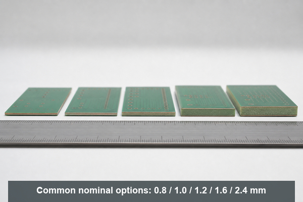
Final Results The finished board achieved stable current carrying capacity, improved heat distribution and better mechanical reliability. The sample passed customer validation and moved to batch production. This project showed that heavy copper large PCB fabrication should combine electrical design, heat control, flatness management and assembly support from the start.
What Large PCB Manufacturing Services Can EBest PCB Provide?
EBest PCB provides one-stop support for large PCB projects, from engineering review to finished PCB assembly. This helps customers reduce supplier communication, shorten project transfer time and control production risk.
PCB design review: We review board size, stack-up, copper balance, material, drill design and assembly risk before production.
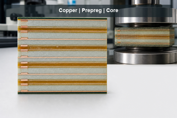
Large PCB prototype: We support sample production for oversized PCB, heavy copper PCB, multilayer PCB and special material boards.
Mass production: We support batch production with a monthly capability of 260,000 square feet / 28,900 square meters.
Component sourcing: We help prepare components based on customer BOM requirements for PCBA orders.
PCB assembly: We provide SMT assembly, through-hole assembly, connector soldering, functional testing and final inspection.
Expedited service: For suitable urgent boards, shipment can be supported within 24 hours after production details are confirmed.
Our product capability covers FR4 PCB, multilayer PCB, metal core PCB, ceramic PCB, flexible PCB, rigid-flex PCB, high frequency PCB, heavy copper PCB, HDI PCB, high Tg PCB and impedance control PCB.
Why Choose EBest PCB as Large PCB Manufacturer in China?
Choosing EBest PCB helps customers reduce design risk, save communication time and move from prototype to production with stronger control.
Lower project risk: With 20+ years of PCB experience, our team can review large board risks before production, including warpage, copper balance, thickness, hole design and assembly handling.
Faster project transfer: PCB design review, prototype, mass production, component sourcing and PCB assembly can be handled through one supplier, reducing repeated communication between different vendors.
Stronger production support: With monthly capability of 260,000 square feet / 28,900 square meters, we can support both sample verification and batch orders.
More material choices: Customers can choose FR4, high Tg FR4, metal core, ceramic, flexible, rigid-flex, high frequency and heavy copper structures according to project needs.
Better compliance support: Certifications including IATF 16949, ISO 9001:2015, ISO 13485:2016, AS9100D, REACH, RoHS and UL help support automotive, medical, aerospace, industrial and general electronics projects.
Clearer delivery path: Expedited service is available for suitable urgent boards, helping customers handle tight project schedules.
For buyers, the value is simple: one China source factory, fewer project delays, clearer engineering support and more stable production control.
FAQs About Large PCB Boards
Q1: What files should I send for a large PCB quote? A1: Please send Gerber files, drill files, board thickness, copper weight, material, surface finish, quantity and delivery request. For PCBA orders, also send BOM, CPL and testing requirements. Complete files help shorten quotation time and reduce production misunderstanding.
Q2: Can EBest PCB help review my design before production? A2: Yes. EBest PCB can review board size, stack-up, copper balance, hole design, spacing, material and assembly risk before production. This helps customers find manufacturability problems before they become prototype or batch defects.
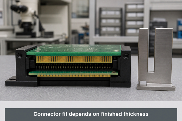
Q3: Can I start with samples before mass production? A3: Yes. You can start with large PCB prototype production to verify size, flatness, copper performance, soldering and function. After sample approval, the project can move to batch production with confirmed process settings.
Q4: Can EBest PCB source components for PCBA orders? A4: Yes. EBest PCB supports component sourcing based on customer BOM requirements. This helps customers reduce purchasing workload and keep PCB fabrication, component preparation and assembly in one project flow.
Q5: How fast can urgent boards be delivered? A5: For suitable urgent boards, EBest PCB can support expedited service, and some boards can be shipped within 24 hours after all files, materials and production details are confirmed. Actual timing depends on board structure and process difficulty.
Q6: What certifications does EBest PCB have? A6: EBest PCB is supported by IATF 16949, ISO 9001:2015, ISO 13485:2016, AS9100D, REACH, RoHS and UL. These certifications help customers meet project requirements in automotive, medical, aerospace, industrial and electronic products.
Q7: What PCB types can EBest PCB manufacture? A7: EBest PCB can manufacture FR4 PCB, multilayer PCB, metal core PCB, ceramic PCB, flexible PCB, rigid-flex PCB, high frequency PCB, heavy copper PCB, HDI PCB, high Tg PCB and impedance control PCB.
Q8: Is EBest PCB a factory or a trading company? A8: EBest PCB is positioned as a China source factory for custom PCB and PCBA solutions. Customers can work with one team for design review, prototype, mass production, component sourcing and PCB assembly.
Q9: Can EBest PCB support regulated industry projects? A9: Yes. With certifications such as IATF 16949, ISO 13485:2016 and AS9100D, EBest PCB can support projects in automotive, medical, aerospace and industrial fields. Final requirements should be confirmed by customer drawings and specifications.
Q10: How can I reduce risk before placing a batch order? A10: Start with complete files, request design review, build samples, test the board and confirm assembly performance before mass production. This process is safer for oversized boards because size, flatness and handling risks can be checked early.
A reliable large PCB project needs early design review, suitable material selection, stable fabrication, controlled assembly and clear delivery planning. EBest Circuit helps customers reduce production risk through PCB design review, prototype support, mass production, component sourcing and PCB assembly from our China source factory.
Send your Gerber files, BOM, quantity and technical requirements to sales@bestpcbs.com. Our team will review your large PCB project and provide a practical quotation for manufacturing and assembly.
When people search for cable SNR, they usually want to know whether a coaxial cable signal is clean enough. In simple terms, SNR shows how much useful signal remains above the noise. A higher SNR usually means fewer errors and more stable communication.
For PCB and PCBA customers, the practical focus is not only the SNR number. It is the product-side RF path after the signal enters the board: RF connector, connector-to-PCB transition, 75Ω controlled impedance trace, grounding, and PCBA assembly quality. This article explains cable SNR from the perspective of PCB layout and PCBA manufacturing.
What Is Cable SNR?
Cable SNR means cable signal-to-noise ratio. It compares the useful signal in a coaxial cable system with unwanted noise. The value is measured in dB.
A simple way to understand it is:
Cable SNR = useful signal compared with noise
When SNR is high, the receiver can separate data from noise more easily. When SNR is low, the useful signal is too close to the noise floor. This may lead to packet loss, uncorrectable errors, unstable speed, or connection drops.
In this article, cable SNR refers to the signal quality commonly checked at the coaxial cable input of cable communication equipment. The point is not to discuss the network side in depth. The point is to understand how the product-side RF input path should be kept clean and consistent.
What Is a Good Cable SNR?
A good cable SNR is commonly 30 dB or higher in many cable communication applications. Values in the mid-to-upper 30s usually provide better margin. The final requirement should always follow the customer’s product specification, chipset guide, test requirement, or approved design file.
Cable SNR
General Meaning
Below 25 dB
Poor or unstable
25–30 dB
Marginal
30–35 dB
Acceptable to good
35–40 dB
Good
40 dB+
Strong, if stable
For a PCB or PCBA project, one good prototype reading is not enough. The product should keep stable RF performance after PCB fabrication, connector soldering, shield-can assembly, mechanical stress, and batch production.
What Do SNR, Downstream Power, and Upstream Power Mean?
Cable signal pages often show SNR, downstream power, and upstream power together. These terms are related, but they are not the same.
Item
Simple Meaning
Why It Matters
SNR
Signal cleanliness
Shows signal margin over noise
Downstream power
Signal entering the device
Too high or too low may affect reception
Upstream power
Signal sent back by the device
High value may mean the device is transmitting harder
In simple terms, SNR tells signal quality, while power tells signal level.
A device may receive enough signal power but still have poor SNR if the signal path is noisy. For PCB and PCBA projects, this distinction matters because the product must preserve both signal level and signal cleanliness after the RF signal enters the board.
Why Does Cable SNR Matter to PCB and PCBA Customers?
Cable SNR matters to PCB and PCBA customers because product-side implementation can weaken signal quality. Even when the incoming cable signal is acceptable, the PCB input path may still introduce loss, reflection, poor grounding, or assembly variation.
For a cable communication PCB or PCBA project, customers usually care about these questions:
Can the RF connector be mounted reliably?
Can the connector-to-PCB transition stay clean?
Can the 75Ω impedance path be controlled in production?
Can grounding reduce unnecessary noise coupling?
Can PCBA assembly keep connector quality consistent across batches?
These are the areas a PCB and PCBA manufacturer can support. The manufacturer does not replace RF system design. Its role is to manufacture and assemble the approved design accurately and consistently.
Why Is 75Ω Common in Cable Input Paths?
Many coaxial cable communication systems use a 75Ω environment. This is common in cable TV, CATV, video transmission, and cable input applications. It is different from many WiFi, cellular, and general RF module paths, where 50Ω is more common.
This does not mean every RF path should be 75Ω. It means the impedance should match the system it belongs to.
In cable input applications, the cable is usually not selected like a generic RF test cable. Many cable TV, CATV, and cable input systems use 75Ω coaxial cable, while many RF modules, WiFi devices, and lab instruments use 50Ω coaxial cable. The PCB input path should match the impedance environment defined by the customer’s product design. For this article, the focus is not cable selection, but how the product-side RF connector and PCB input path preserve the approved impedance.
For PCB layout, the key point is not to guess between 50Ω and 75Ω. The correct impedance should follow the customer’s chipset reference design, RF input requirement, connector datasheet, PCB stack-up, and approved layout file.
If the external cable interface is based on 75Ω, the connector-to-PCB transition and PCB input trace usually need to preserve that 75Ω path unless the customer’s design specifies otherwise.
What Is the 75Ω RF Input Path on PCB?
The 75Ω RF input path is the product-side signal route after the cable signal enters the board. It usually starts from the RF connector and continues toward the RF input circuit.
This is the core of the article. Cable SNR is the signal-quality reading. The 75Ω PCB input path is one product-side area that can affect whether the approved hardware performs consistently.
Why Does RF Connector Layout Matter on PCB?
RF connector layout matters because the connector is the bridge between the cable signal and the PCB signal path. Poor execution can create impedance discontinuity, reflection, extra loss, or unstable grounding.
For PCB layout execution, the connector area should follow the customer’s approved files, including the connector datasheet, recommended footprint, PCB stack-up, impedance requirement, and layout guide.
Key points include:
Footprint accuracy Pad size, drill, plating, solder mask opening, and mechanical land pattern should match the approved connector drawing.
Connector-to-trace transition The path from connector pin to RF trace should be short and clean. Avoid unnecessary stubs and sudden geometry changes.
Ground pad placement Ground pads around the connector support shielding and return path continuity.
Ground via placement Ground vias near the connector shell and RF transition can help support a stable return path when placed according to layout requirements.
Shell grounding The connector body should connect reliably to ground.
Mechanical support RF connectors may face pulling, twisting, and repeated plugging. The footprint should support both electrical and mechanical reliability.
This is PCB layout execution, not complete RF design. A PCB layout team should implement the connector area based on customer-approved requirements. It should not claim RF connector launch redesign unless that service is truly provided.
How Does Controlled Impedance Protect Cable SNR?
Controlled impedance helps keep the RF input path predictable. For cable input PCB projects, this often means maintaining a 75Ω signal path from the RF connector toward the input circuit.
The correct impedance should come from the customer’s schematic, chipset reference, connector datasheet, PCB stack-up, or approved layout file.
75Ω controlled impedance depends on:
PCB stack-up
Dielectric thickness
Copper thickness
Trace width
Reference ground plane
Solder mask effect
Etching tolerance
Impedance test coupon
If the stack-up changes, impedance may shift. If etching control is poor, trace width may move out of tolerance. If the reference ground is interrupted, the return path becomes less predictable.
A PCB manufacturer can support this by reviewing the stack-up, calculating impedance with actual production materials, controlling lamination and etching, and providing impedance testing when required.
For the customer, the value is simple: the 75Ω path should not only be correct in the design file. It should remain controlled in production.
How Does Grounding Affect the RF Input Path?
Grounding affects the RF input path because RF signals need a stable return path. Poor grounding can increase reflection, coupling, and noise sensitivity.
For PCB layout and PCBA production, the grounding focus should be practical:
Connector shell grounding The connector body should have a reliable ground connection.
Reference plane continuity The RF trace should not cross unnecessary ground cuts, slots, or broken reference planes.
Ground via stitching Ground vias near the RF connector and input path can help maintain a cleaner return path when used according to layout requirements.
Shield-can ground pads If the design uses a shield can, its ground pads should be placed and soldered correctly.
Return path control The RF signal and its return path should stay close and predictable.
Grounding cannot solve every cable SNR problem. If the incoming cable line is noisy, PCB grounding alone cannot fix it. But poor grounding can make a good design perform worse than expected.
How Does PCBA Assembly Affect RF Connector Reliability?
PCBA assembly quality strongly affects RF connector reliability. For RF and coaxial interfaces, soldering quality, alignment, grounding, and mechanical strength all matter.
Key assembly points include:
Connector alignment F-type, SMA, SMB, MCX, board-edge, or custom RF connectors should be placed accurately.
Solder wetting Connector ground pads, center pins, and mechanical tabs should have proper solder wetting.
Ground pad soldering RF connector ground pads are part of the shielding and return path. Weak soldering may reduce stability.
Mechanical anchor strength Cable connectors may face pulling, twisting, and repeated plugging. Anchor points must be reliable.
Shield-can soldering Lifted edges, solder gaps, or excessive solder can affect shielding and consistency.
Inspection Visual inspection, AOI, and X-ray when needed can help identify placement shift, solder defects, hidden joints, and connector issues.
Functional test support If the customer provides test firmware, fixtures, RF test method, or acceptance criteria, the PCBA factory can support defined production testing.
For communication products, one working prototype does not guarantee mass-production stability. Customers need repeatable soldering, controlled process parameters, consistent connector handling, and traceable inspection records.
FAQs About Cable SNR
Q1: What is a good cable SNR?
A good cable SNR is commonly 30 dB or higher in many cable communication applications. Mid-to-upper 30s usually provide better stability.
Q2: Is 29 dB SNR good?
29 dB is usually marginal. It may work, but the margin is limited. If noise rises or the signal path fluctuates, errors or unstable speed may appear.
Q3: Is cable SNR the same as downstream power?
No. Cable SNR measures signal quality compared with noise. Downstream power measures the signal level entering the device.
Q4: What does upstream power mean?
Upstream power is the signal level the device sends back to the network. If it is high, the device may be working harder to transmit.
Q5: Can PCB layout affect cable SNR?
PCB layout can affect the product-side RF path through connector transition, 75Ω impedance control, grounding, and return path continuity. It cannot control the external cable network.
Q6: Can PCBA quality affect RF connector performance?
Yes. Connector soldering, ground pad quality, shield-can soldering, inspection, and functional testing can affect production consistency and RF connector reliability.
In conclusion, cable SNR shows how clean a cable signal is compared with noise. For many cable input applications, 30 dB or higher is a practical baseline.
For PCB and PCBA customers, the main concern is the 75Ω RF input path. RF connector layout, controlled impedance, grounding, and connector assembly quality can all affect whether the approved design performs consistently in production.
If you are developing a cable input PCB or RF connector PCBA project, you are welcome to send your schematic, BOM, Gerber files, stack-up, impedance requirements, connector datasheets, and assembly drawings to sales@bestpcbs.com. Best Technology will review them carefully and help evaluate a suitable PCB manufacturing and turnkey PCBA assembly approach.
PCB components identification is the process of recognizing every electronic part mounted on a PCB by checking board markings, reference designators, PCB symbols, package shape, body codes, polarity marks, footprint and BOM data. It helps users understand what each component is, what it does and whether it matches the design.
For repair, inspection, reverse engineering, component sourcing and PCBA production, one visual clue is never enough. A reliable PCB components identification method combines PCB silkscreen, component markings, printed circuit board parts list, schematic, test tools and production inspection records. This guide explains how to identify PCB components clearly and practically.
What Is PCB Components Identification?
PCB components identification means matching each physical part on a PCB with its type, value, package, polarity, rating and circuit function. It helps users recognize resistors, capacitors, inductors, diodes, transistors, ICs, connectors, fuses, relays and switches.
The process usually starts from visible PCB markings. Then the component body code, reference designator, package shape, pin count, PCB symbol and surrounding circuit are checked. If design files are available, the BOM and schematic provide stronger confirmation.
In real PCB assembly, many SMD parts are too small to show full markings. Some ceramic capacitors have no printed code, and some ICs only show short top marks. Therefore, PCB components identification should combine visual checking, documentation and testing.
Why Is PCB Components Identification Important?
Accurate PCB components identification reduces repair errors, wrong sourcing, assembly defects and production delays. It is important for PCB repair, prototype debugging, incoming inspection, SMT assembly, quality control and mass production.
Main benefits include:
Faster troubleshooting when a PCB fails during testing.
Better replacement accuracy when damaged parts must be changed.
Lower BOM mismatch risk before SMT production.
Improved first article inspection before batch assembly.
Stronger traceability for component batches and approved substitutes.
Clearer communication between engineers, buyers and PCB suppliers.
For purchasing teams, correct PCB components identification also helps avoid wrong part numbers, unsuitable replacements and counterfeit risks. In dense PCBA projects, it supports smoother quotation, sourcing and production approval.
What Tools Are Needed for PCB Board Components Identification?
PCB board components identification requires visual tools, electrical tools, design documents and inspection equipment. A simple repair may only need a microscope and multimeter, while production-level PCB components identification often requires BOM review, AOI, X-ray and functional testing.
Tool
Best Use
What to Check
Practical Note
Magnifier
Large parts and board text
Silkscreen, polarity, damage
Good for quick first inspection
Microscope
Small SMD parts
Top code, cracks, solder joints
Useful for 0201, 0402, QFN and fine-pitch ICs
Multimeter
Basic electrical checks
Resistance, continuity, diode direction
Check unpowered circuits first
LCR meter
Passive components
Capacitance, inductance, ESR
In-circuit readings may be affected
Bench power supply
Controlled power-up
Current draw, short protection
Set current limit before testing
Thermal camera
Fault location
Hot ICs, shorted rails, overload
Helpful for failed boards
Datasheet
Technical confirmation
Pinout, package, rating
Match top code and package together
BOM
Exact part verification
MPN, value, package, substitutes
Most important for PCBA sourcing
AOI
SMT inspection
Missing parts, wrong polarity, offset
Common in assembly production
X-ray
Hidden solder inspection
BGA, QFN, voids, bridges
Needed for hidden pads
ICT
Electrical production test
Nets, shorts, component presence
Useful for batch control
Functional tester
Final product behavior
Real operating performance
Confirms the board works as designed
Before applying power, inspect the PCB for burned marks, shorted rails, reversed parts and damaged solder joints. For production projects, the best result comes from combining manual inspection, BOM checking and automated inspection instead of using only one tool.
How to Identify PCB Components on a Circuit Board?
To identify PCB components on a circuit board, follow a fixed order from board information to final confirmation. This keeps PCB components identification clear, repeatable and safer than guessing from appearance only.
Step 1: Check the PCB model and revision. Start with the board number, revision code, date code and assembly side. Board revision matters because the same reference designator may use different values or packages in different versions.
Step 2: Read the silkscreen and PCB symbols. Look for R, C, L, D, Q, U, J, F, SW, TP and polarity signs. PCB symbols can show whether a part is related to resistance, capacitance, diode direction, IC pin 1, connector orientation or test access.
Step 3: Inspect package shape and footprint. Check whether the part is SMD or through-hole. Then review body size, pad layout, pin pitch, number of terminals, thermal pad and mounting direction. A correct value with the wrong footprint may still fail assembly.
Step 4: Read the component marking. Use a microscope to check SMD codes, logos, stripes, dots, notches, printed values and date codes. A short SMD code should not be used as final proof because it may not be unique.
Step 5: Confirm with documents and testing. Compare the part with the BOM, schematic, datasheet and placement file. When needed, use a multimeter, LCR meter or diode mode to verify the component safely.
How to Read PCB Component Markings and Codes?
PCB component markings and codes are printed on the component body and should be read with package type, polarity, logo and circuit position. In PCB components identification, a short code alone is not enough for final confirmation.
Part
Marking
Example
Resistor
3-digit or 4-digit code
103, 4701
Capacitor
Value code or no marking
104, 10µF
Diode
Stripe, logo or code
Cathode band
Transistor
Short SMD code
SOT-23 code
IC
Top mark, logo, date code
Part code
Fuse
Current rating
2A, F2A
Relay
Coil voltage and contact rating
5V, 12V
For PCB component identification code reading, the same short code may appear on parts from different manufacturers. Therefore, package size, pin count, logo, circuit function and datasheet matching should be checked together. This makes a PCB component markings guide more useful in repair, inspection and PCBA production.
PCB Component Identification Chart
A PCB Component Identification Chart should help users check component type, board clue, body marking, package, polarity, rating and confirmation method in one place. It is not just a simple list of component names. It works as a practical PCB components identification guide before repair, sourcing or assembly.
Component
Designator
Board Clue
Body Clue
Package Clue
Confirm By
Resistor
R
Near signal or divider circuit
Number code or color bands
2 terminals, chip or axial
Resistance value, BOM
Ceramic capacitor
C
Near IC power pins or filters
Often blank or small code
2-terminal MLCC chip
Capacitance, BOM
Electrolytic capacitor
C
Power input or filtering area
Value, voltage, stripe
Cylindrical or can type
Polarity, capacitance
Inductor
L
Near DC-DC converter or filter
Code or blank body
Coil, ferrite or molded block
Inductance, current rating
Diode
D
Direction mark on silkscreen
Stripe or short code
2-terminal SMD or axial
Diode mode, datasheet
Transistor
Q
Switching or control area
Short SMD code
3-pin or power package
Pinout, datasheet
MOSFET
Q
Power switching area
Code and logo
SOT, TO, DFN or power package
Gate, drain, source check
IC
U / IC
Pin-1 mark or outline
Top mark, logo, date code
Multi-pin package
Datasheet, BOM
Connector
J / P / CN
Pin number or outline
Usually no value code
Header, socket, terminal
Pin count, pitch, mating part
Fuse
F
Power input path
Current rating or code
SMD, cartridge, resettable
Continuity, current rating
Relay
K / RY / RL
Load switching area
Coil voltage, contact rating
Box package
Coil and contact datasheet
Switch
SW
User input area
Type or blank body
Tactile, slide, DIP
Footprint, operation test
This chart is most useful when combined with the printed circuit board parts list, schematic, datasheet and test results. For field repair and supplier review, PCB components identification becomes more accurate when the chart is used as a checklist instead of a guess sheet. For unknown parts, use it to narrow the component group first, then confirm value, rating and package through documents or measurement.
How to Identify Passive Components on a PCB?
Passive components include resistors, capacitors and inductors. They do not amplify signals, but they strongly affect current, voltage, filtering, timing and power stability.
Step 1: Start with the reference designator. R usually means resistor, C means capacitor, and L means inductor. This quickly separates passive parts from semiconductors, connectors and ICs during PCB components identification.
Step 2: Check the package and appearance. Resistors and ceramic capacitors may both look like small rectangular chips, so do not judge by shape alone. Inductors are often larger, darker, magnetic or coil-shaped, especially in power circuits.
Step 3: Read the value mark if available. Resistors may show 103, 472 or 1001. Ceramic capacitors may have no marking. Electrolytic capacitors usually show capacitance and voltage. Inductors may show a value code, but many power inductors are unmarked.
Step 4: Confirm rating and circuit role. Use the BOM, LCR meter or datasheet to check resistance, capacitance, inductance, voltage rating, current rating, tolerance and temperature range. A correct value with the wrong voltage or current rating can still cause failure. This keeps PCB components identification focused on real electrical performance, not only visual appearance.
How to Identify Semiconductor Components on a PCB?
Semiconductor components include diodes, LEDs, transistors, MOSFETs, regulators, TVS diodes and ESD protection devices. They must be checked carefully because polarity, pinout and rating directly affect circuit safety.
Step 1: Check the designator. D usually means diode, LED or TVS diode. Q usually means transistor or MOSFET. Some regulators may use U because they are IC-style devices.
Step 2: Read polarity and body marks. A diode often has a cathode stripe. LEDs may have a flat edge, dot or pad mark. Transistors and MOSFETs often use short SMD codes, so the code must be checked with package and circuit location.
Step 3: Use circuit position to narrow the function. A SOT-23 part near a connector may be ESD protection. A similar SOT-23 part near a power circuit may be a regulator, transistor or MOSFET driver. Position gives important context in PCB components identification.
Step 4: Confirm by datasheet or test. Use diode mode, continuity checks and datasheet comparison before replacement. For power semiconductors, also confirm voltage rating, current rating, package heat dissipation and pinout.
How to Identify ICs and Microcontrollers on a PCB?
ICs and microcontrollers are identified by reference designator, top marking, logo, package type, pin count, pin-1 mark and surrounding circuit. They usually use U or IC designators.
Step 1: Read the top marking under magnification. Check the printed code, manufacturer logo and date code. Some ICs show a full part number, while others only show a shortened top mark.
Step 2: Confirm the package type. Check whether the IC is SOIC, QFN, QFP, BGA, LGA, DIP or another package. Package size, pitch and pin count can quickly narrow the possible device family.
Step 3: Find pin 1 before any replacement. Look for a dot, notch, bevel, chamfer or PCB pin-1 mark. Wrong orientation can damage the IC, short power rails or stop the board from booting.
Step 4: Study the surrounding circuit. Microcontrollers are often connected to crystals, reset circuits, programming headers, decoupling capacitors and communication lines. Power ICs are often near inductors, diodes, MOSFETs and large capacitors.
Step 5: Confirm with BOM and datasheet. Do not source or replace an IC from the top mark alone. Always confirm package, pinout, voltage, memory size, temperature grade and firmware requirements when applicable. In IC sourcing, PCB components identification should also consider firmware, programming status and lifecycle risk.
How to Identify Connectors, Fuses, Relays and Switches on a PCB?
Connectors, fuses, relays and switches are usually recognizable by shape, but rating, pinout and mechanical fit still need confirmation. These parts connect the PCB to power, signals, users or external equipment.
Step 1: Check the designator. Connectors may use J, P or CN. Fuses use F. Relays may use K, RY or RL. Switches usually use SW.
Step 2: Identify the mechanical structure. For connectors, check pin count, pitch, latch direction, mounting angle, height and mating style. For switches, check whether the part is tactile, slide, DIP, pushbutton or rotary.
Step 3: Confirm electrical rating. Fuses require current and voltage rating. Relays require coil voltage and contact rating. Connectors require current capacity, insulation distance and mating reliability.
Step 4: Match the footprint and assembly height. Do not replace these parts by appearance only. Pin layout, body size, housing direction, mechanical strength and height must match the PCB and enclosure design. For PCB components identification in sourcing work, mechanical fit and electrical rating must be checked together.
How to Identify PCB Component Polarity and Pin Orientation?
PCB component polarity and pin orientation must be checked before repair, replacement or assembly because reverse mounting can damage the circuit. This is critical for diodes, LEDs, electrolytic capacitors, tantalum capacitors, ICs, connectors and modules.
Step 1: Check the component body mark. Look for a diode stripe, LED flat edge, capacitor stripe, IC dot, notch, bevel or connector key. These marks usually show direction or pin 1.
Step 2: Compare with PCB silkscreen. The PCB may show +, -, pin 1, a shaded pad, diode symbol or connector outline. The board marking should match the component direction.
Step 3: Confirm with datasheet. Some polarity marks are manufacturer-specific. Electrolytic capacitors often mark the negative side, while many tantalum capacitors mark the positive side.
Step 4: Stop if marks conflict. If the body mark, PCB symbol and datasheet do not match, do not power the PCB. Check the BOM, schematic and assembly drawing first. Correct polarity checking is a key part of reliable PCB components identification.
How to Identify Unknown or Unmarked PCB Components?
Unknown or unmarked PCB components should be identified by reference designator, package, footprint, circuit location, measurement, BOM comparison and similar board analysis. Guessing from shape alone can lead to wrong repair or sourcing.
Step 1: Check the nearby reference designator. The designator gives the first clue. R, C, L, D, Q, U, F, J and SW point to different component groups.
Step 2: Inspect package, pins and footprint. Package size, terminal count, thermal pad, pad layout and orientation marks can narrow the component type. A two-terminal part may be a resistor, capacitor, diode, fuse or inductor, so the circuit position matters.
Step 3: Study nearby circuits. A part near power input may be protection, filtering or regulation. A part near a crystal may support timing. A part near a connector may be ESD protection or signal conditioning.
Step 4: Compare with documents or a known board. Use the BOM, schematic, placement file or a working sample to confirm the part. If the board is damaged, compare the failed area with an undamaged board revision.
Step 5: Test before replacement. For burned parts, check the root cause first. The damaged component may be the result of a short, overload or reverse polarity, not the original failure source. In difficult cases, PCB components identification should be reviewed before any replacement decision.
What Common Mistakes Happen During PCB Components Identification?
The most common mistakes during PCB components identification come from relying on one clue, ignoring ratings or skipping document checks. Each mistake can lead to wrong repair, wrong sourcing or failed PCBA assembly.
Mistake: Treating reference designators as values. Solution: Use R1, C2 or U3 only as location labels. Confirm value and part number through BOM, schematic or measurement.
Mistake: Trusting one SMD code as final proof. Solution: Check package size, pin count, logo, circuit position and datasheet because short codes are not globally unique.
Mistake: Ignoring polarity and pin orientation. Solution: Compare body marks, PCB silkscreen and datasheet before assembly or replacement.
Mistake: Replacing a burned part directly. Solution: Check power rails, nearby loads, shorts and root cause before installing a new component.
Mistake: Matching components by appearance only. Solution: Confirm voltage, current, tolerance, package, footprint, height and lifecycle status.
Mistake: Using substitutes without approval. Solution: Review approved vendor list, BOM notes and customer requirements before changing any component.
FAQs About PCB Components Identification
Q1: What is the difference between PCB silkscreen and solder mask? A1: PCB silkscreen is the printed text or symbol layer that shows reference designators, polarity marks, logos and assembly notes. Solder mask is the colored protective coating over copper. Silkscreen helps identification, while solder mask protects copper and defines exposed soldering areas. They work together but serve different purposes.
Q2: Can component values be measured directly on the PCB? A2: Sometimes yes, but in-circuit measurement may be affected by parallel paths, connected IC pins or surrounding components. A resistor, capacitor or inductor may read differently while still mounted. For critical checking, compare with the BOM or lift one terminal carefully before measurement if the board design allows it.
Q3: What does DNP, DNI or NC mean in a BOM? A3: DNP means do not populate, DNI means do not install, and NC usually means no connect or not connected depending on the context. These notes tell the assembly factory whether a component position should remain empty. Always check the BOM notes before assuming a missing component is an assembly defect.
Q4: Why does a replacement component fit but still fail? A4: A component may fit the footprint but still have the wrong voltage rating, current rating, tolerance, temperature range, polarity, pinout or internal structure. Mechanical fit does not guarantee electrical compatibility. Before replacement, check the full datasheet and BOM requirement instead of relying only on package size. This is a common PCB components identification issue in repair and sourcing work.
Q5: How do test points help PCB troubleshooting? A5: Test points give access to important nets such as power rails, ground, reset, communication lines or programming signals. They help technicians check voltage, continuity and signal behavior without touching tiny component pins. In production, test points also support ICT, functional testing and faster fault isolation.
Q6: Can conformal coating affect PCB component identification? A6: Yes. Conformal coating can cover component markings, polarity signs, small SMD codes and solder joints. Microscope inspection, UV light or controlled coating removal may be required. Coating removal should be done carefully because aggressive scraping can damage pads, solder joints or component bodies.
Q7: How do counterfeit components affect PCBA reliability? A7: Counterfeit components may have fake markings, poor internal structure, wrong die, weak plating or unstable electrical performance. They can pass visual inspection but fail during temperature, load or long-term operation. Reliable sourcing, approved suppliers and traceable purchasing records are important for PCBA reliability.
Q8: What files should I prepare before asking for PCBA quotation? A8: Prepare Gerber files, BOM, CPL or placement file, schematic if available, assembly drawings, testing requirements and clear notes for special parts. Complete files help the factory check component availability, package match, polarity, substitutes and production risks. This also makes quotation faster and more accurate.
Q9: Why is board revision important for component checking? A9: Different PCB revisions may use different component values, packages, footprints or approved substitutes. The same reference designator may not have the same value across different revisions. Always check the PCB revision before comparing BOM data, repairing a board or approving PCBA production.
Q10: How can buyers reduce BOM sourcing risk? A10: Buyers can reduce risk by confirming manufacturer part numbers, lifecycle status, approved alternatives, minimum order quantity, lead time and material traceability. For mass PCBA projects, BOM review should happen before production starts. This helps avoid obsolete parts, wrong substitutes and urgent sourcing changes.
Q11: What should be checked when a component is missing from a PCB? A11: First check whether the BOM marks that position as DNP, DNI or optional. Then confirm the board revision, placement file and assembly drawing. A missing part is not always a defect. Some positions are intentionally left empty for configuration, testing, cost control or different product versions.
Q12: How can a factory prevent wrong component loading during SMT assembly? A12: A factory can reduce wrong loading by reviewing the BOM, verifying reels, checking feeder setup, using barcode control and performing first article inspection. AOI and functional testing provide additional protection after placement and soldering. Good material traceability also helps locate problems quickly if a batch issue appears.
PCB components identification is not just a repair skill. It is a practical quality-control method that connects PCB symbols, board markings, component codes, package shape, footprint, polarity, BOM data, testing and production records. The key technical point is clear: confirm every important component through multiple clues before repair, sourcing or assembly.
For PCBA projects, correct PCB components identification helps prevent wrong parts, wrong polarity, wrong substitutes and delayed production. EBest Circuit supports PCB fabrication, PCBA assembly, BOM review, component sourcing, SMT assembly, AOI, X-ray, ICT, functional testing and global delivery from our China source factory. Send your Gerber files, BOM and PCBA requirements to sales@bestpcbs.com for a fast quotation and reliable component sourcing support.
When people search for what is a good SNR for WiFi, they usually want a clear number. Is 15 dB enough? Is 20 dB good? Is 30 dB ideal? In simple terms, WiFi works better when the useful signal is much stronger than the surrounding noise. That is why signal bars alone are not enough. A device may show strong signal strength, but if the noise floor is high, the real connection can still be slow, unstable, or easy to drop.
For wireless products, WiFi SNR is also related to how the device is built. PCB layout, RF trace routing, grounding, antenna keep-out handling, controlled impedance, power noise control, SMT assembly, RF connector soldering, and shield-can assembly can all affect final performance. This article explains WiFi SNR in a practical way and focuses on what a PCB and PCBA manufacturer can support. If you are developing a WiFi PCB or PCBA project, you are welcome to send your files and requirements to sales@bestpcbs.com for a careful review.
What Does SNR Stand for in WiFi?
SNR stands for signal-to-noise ratio. In WiFi, it shows the difference between the useful wireless signal and the surrounding noise. It is usually measured in decibels, written as dB.
A simple way to understand it is:
SNR = Signal Strength – Noise Floor
SNR is not the same as signal strength. Full signal bars do not always mean a high SNR.
For example:
Signal Strength
Noise Floor
SNR
WiFi Quality
-65 dBm
-90 dBm
25 dB
Good
-65 dBm
-80 dBm
15 dB
Weaker
In both cases, the WiFi signal strength is the same: -65 dBm. The real difference is the noise floor. When the surrounding noise rises from -90 dBm to -80 dBm, the SNR drops from 25 dB to 15 dB.
This is why a device can be close to the router but still have a poor WiFi experience. Nearby WiFi networks, Bluetooth devices, microwave ovens, switching power supplies, motors, displays, and other noise sources can raise the noise floor. When that happens, RSSI or signal bars may still look good, but the actual connection can become slow or unstable.
So, when evaluating WiFi quality, do not only look at RSSI or signal bars. SNR gives a clearer view of how clean the WiFi signal is compared with the surrounding noise.
For wireless products, this matters because the end user does not care whether the problem comes from the router, enclosure, PCB layout, power noise, antenna position, or PCBA process. They only notice unstable connection, slower response, packet loss, or shorter range.
What Is a Good SNR for WiFi?
A good SNR for WiFi is usually around 20 dB or higher for normal data communication. For better stability, 25–30 dB is a stronger target range. If the SNR is above 30 dB, the WiFi connection usually has a comfortable margin over noise.
In practical terms:
SNR Rating
General Meaning
Below 10 dB
Poor
10–15 dB
Weak
15–20 dB
Fair
20–25 dB
Good
25–30 dB
Very good
30 dB+
Excellent
So, what is a good signal to noise ratio for WiFi? For many wireless products, 20 dB or higher is a useful baseline. For products that need better reliability, such as WiFi cameras, IoT gateways, smart control devices, medical monitoring products, and industrial terminals, a higher SNR is preferred.
However, there is no single ideal SNR for every product. A battery-powered sensor, a smart plug, a WiFi camera, and an industrial gateway do not have the same communication load or installation environment.
A simple sensor may only send small data packets. A WiFi camera needs more stable bandwidth. An industrial gateway may need reliable communication in a noisy electrical environment. That is why the ideal SNR depends on the product application, wireless module, antenna type, enclosure, power system, and final test environment.
For PCB and PCBA projects, the target should come from the customer’s product requirement, wireless module datasheet, RF test plan, and application environment. The PCB layout and manufacturing team can then support the project by following the approved stack-up, impedance requirement, grounding rule, antenna keep-out rule, and assembly instruction.
What Do Different SNR Values Mean for WiFi Quality?
Different SNR values show how much margin the WiFi signal has over the surrounding noise. The higher the SNR, the easier it is for the receiver to separate useful data from unwanted interference.
WiFi SNR
Quality Level
Practical Meaning
0–10 dB
Poor
Unstable connection
10–15 dB
Weak
Basic connection only
15–20 dB
Fair
Usable, but limited margin
20–25 dB
Good
Suitable for normal WiFi use
25–30 dB
Very Good
Better stability and speed
30 dB+
Excellent
Strong signal margin
For example, SNR 15 may still support basic WiFi communication, but it is not ideal for stable data transmission. It may work in a clean environment, but the margin is limited. If the noise increases, the device moves farther from the router, or the enclosure weakens the antenna performance, the connection may become unstable.
SNR 6 is usually too low. At this level, the useful signal is very close to the noise floor. The device may still connect, but slow speed, packet loss, retransmission, or disconnection can occur.
A high SNR is usually better because the receiver has a cleaner difference between the useful signal and the noise. A high signal-to-noise ratio does not solve every WiFi issue, but it gives the system more room to work.
For wireless product development, the goal is not only to reach a good value in a perfect lab condition. The product should also maintain enough margin after enclosure assembly, component tolerance, PCB production, SMT assembly, and real-world operation.
Why Can WiFi Signal Strength Be Good but SNR Still Poor?
A common misunderstanding is that strong WiFi signal means good WiFi quality. This is not always true. If the signal is strong but the noise is also high, the SNR will still be low.
In other words, a device can show full signal bars but still suffer from slow speed, retransmission, packet loss, or unstable connection.
This happens because WiFi quality depends on both sides of the equation:
Signal strength shows how strong the useful WiFi signal is.
Noise floor shows how much unwanted background noise exists.
SNR shows the gap between them.
If the signal is strong and the noise is low, the SNR is good. If the signal is strong but the noise is also high, the SNR becomes worse.
In real products, noise can come from many places:
Neighboring WiFi networks
Bluetooth devices
Microwave ovens
Switching power supplies
DC-DC converters
High-speed digital circuits
Motors, relays, and power drivers
Displays, cameras, USB circuits, and other modules
Poor grounding or noisy return paths
Bad RF connector contact or weak soldering
Some of these issues are outside the PCB factory’s control. For example, the factory cannot control the customer’s router, building structure, wireless channel, firmware, or final installation environment.
But some issues are related to hardware execution. If noisy circuits are placed too close to the WiFi section, if the RF trace has poor reference grounding, if the antenna area is blocked by copper or metal, or if the RF connector is not soldered well, the wireless module may not perform as expected.
That is why WiFi SNR should not be treated only as a router setting. In embedded wireless devices, PCB layout and PCBA quality can affect whether the wireless module works close to its intended performance.
Which PCB Layout Factors Can Influence WiFi SNR?
PCB layout cannot decide the final WiFi SNR alone. The wireless chip, antenna, firmware, enclosure, access point, distance, and environment also matter. However, poor layout can reduce the performance margin of a WiFi device.
In WiFi PCB layout, the following points need careful control:
RF trace path The RF trace should be short, clean, and routed according to the WiFi module datasheet or customer-provided layout guide. If a 50Ω RF path is required, the trace geometry should match the approved stack-up.
Ground reference RF traces need a stable reference plane. Broken ground, unnecessary slots, or poor ground continuity can disturb the return path and increase noise sensitivity.
Noise source placement DC-DC converters, high-speed signals, motors, relays, displays, and large current loops should be kept away from RF-sensitive areas when the layout allows.
Antenna area The antenna keep-out area should remain clear according to the module or antenna layout guide. Copper, ground, components, and metal structures should not be added into this area unless approved.
Via and shielding support Ground stitching vias and shield-can grounding should follow the customer’s layout requirements. These details help create a cleaner local ground environment around RF sections.
A PCB layout team should not replace RF system design. Its practical role is to execute the layout correctly based on the customer’s schematic, datasheet, stack-up, impedance requirement, antenna guide, and mechanical constraints.
For PCB manufacturing, the production side should also protect the layout intent. Line width, copper thickness, dielectric thickness, registration, solder mask opening, via quality, and surface finish can all affect high-frequency reliability when the design is compact or impedance-sensitive.
Why Does Controlled Impedance Matter in WiFi PCB Layout?
Controlled impedance matters because WiFi RF traces work at high frequencies. At 2.4 GHz, 5 GHz, or 6 GHz, the RF path cannot be treated like an ordinary low-speed signal trace.
Many WiFi modules require a 50Ω single-ended RF trace between the module and the antenna connector, chip antenna, or external antenna path. To achieve this, the PCB layout and PCB fabrication process must work together.
Key factors include:
PCB stack-up
Dielectric thickness
Copper thickness
Trace width
Reference ground plane
Solder mask influence
Impedance tolerance
Test coupon requirement
For PCB manufacturing, controlled impedance is not only a drawing requirement. It must be supported by real production control. If the stack-up changes, the RF trace impedance may also change. If trace width, copper plating, or dielectric thickness are not stable, the final RF performance can shift.
This is where a PCB factory can provide practical value. The factory can review the stack-up, calculate impedance based on actual materials, control etching and lamination, and provide impedance testing when required.
For WiFi PCB projects, the customer should provide clear impedance requirements. If the project uses a WiFi module, the module datasheet or layout guide may already define the RF trace structure. The PCB layout should follow those requirements instead of guessing.
For PCBA projects, controlled impedance is only one part of the whole path. The assembly team should also protect the RF-related areas during SMT, reflow, cleaning, inspection, and handling. RF connectors, WiFi modules, antenna connectors, and shield cans should be assembled with consistent quality.
How Should Antenna Keep-Out Areas Be Handled in PCB Layout?
Antenna keep-out is one of the most important layout details in wireless products. It is also an area where the service boundary must be clear.
A PCB layout team can help implement antenna keep-out rules. But antenna design and RF tuning should be handled by the customer’s RF engineer, module supplier, or antenna specialist.
Many WiFi and Bluetooth modules provide layout instructions for antenna position and keep-out areas. These instructions may define board edge distance, copper clearance, ground clearance, component restriction, and nearby metal limitations.
In PCB layout execution, antenna keep-out usually means:
No copper in the defined keep-out area
No components inside the antenna clearance zone
No high-speed traces crossing the antenna area
No ground pour where the module guide forbids it
No shield can or metal part over the antenna area unless approved
Proper distance from batteries, displays, heat sinks, speakers, and metal enclosure parts
The most common mistake is treating the antenna area like normal empty PCB space. It is not. The antenna area is part of the wireless performance structure.
For PCB and PCBA production, the factory should check that the Gerber files follow the keep-out requirements. During assembly, the production team should also avoid adding labels, metal parts, tall components, or unexpected shielding structures that conflict with the antenna zone.
If the customer uses a certified WiFi module, following the module manufacturer’s layout guide is especially important. Poor placement can reduce range, change radiation behavior, or make the final product fail RF validation.
This does not mean the PCB factory is designing the antenna. It means the factory helps preserve the antenna conditions required by the customer’s approved design.
How Does PCB Grounding Affect WiFi Noise?
PCB grounding affects WiFi noise because RF signals need a clear return path. A clean ground reference helps the RF path behave more predictably. A broken or noisy ground structure can increase coupling, radiation, and signal instability.
In WiFi PCB layout, grounding should focus on these points:
Continuous reference plane RF traces should have a solid ground reference. Avoid routing RF traces over ground gaps, plane splits, or large voids.
Short return path The return current should have a nearby path. A long or interrupted return path can create extra noise and unwanted radiation.
Ground stitching vias Proper via stitching around RF sections, board edges, or shield-can areas can help improve local grounding.
Power noise isolation Switching power circuits should be arranged carefully. Poorly placed DC-DC converters or noisy current loops may affect WiFi module stability.
Shield-can grounding If a shield can is used, its grounding pads should be well connected and properly soldered during PCBA production.
Grounding cannot solve every WiFi problem, but it can reduce avoidable layout-related noise. For wireless products, clean grounding is one of the most important details in PCB layout execution.
Grounding quality also depends on manufacturing and assembly. Via reliability, copper plating, solder mask registration, module pad soldering, connector grounding, and shield-can soldering can all affect the final consistency of the product.
A prototype may work during a quick test, but mass production requires repeatability. If grounding-related solder joints or RF connectors vary from board to board, wireless performance may also vary.
What Types of WiFi PCB and PCBA Products Need Good SNR?
Good SNR is important for many wireless products, especially when the device needs stable data transmission, long working distance, or reliable operation in a noisy environment. For PCB and PCBA projects, this often appears in products that combine WiFi modules, RF traces, antenna areas, power circuits, sensors, and control circuits on a compact board.
Common WiFi PCB and PCBA products include:
IoT control boards Smart controllers, wireless sensors, and connected terminals often use compact PCB layouts. Good grounding, antenna keep-out handling, and stable PCBA assembly help support reliable wireless communication.
Smart home device PCBA Smart switches, smart plugs, gateways, lighting controllers, and home automation products need stable WiFi connection in environments with many nearby wireless devices.
Industrial wireless gateways Industrial gateways, monitoring terminals, and control modules may work near motors, power supplies, relays, and metal enclosures. These products need careful PCB layout and strong manufacturing consistency.
WiFi camera and security device PCBA WiFi cameras, access control devices, and security terminals usually require more stable data transmission. Poor SNR may lead to video delay, dropped connection, or unstable upload.
Medical and monitoring device PCBA Wireless monitoring devices need stable communication and clean assembly quality. In these products, consistent soldering, connector reliability, and functional testing are important.
Consumer electronics with WiFi modules Portable devices, audio products, handheld terminals, and appliance control boards may use built-in WiFi modules. The PCB layout should follow module datasheets, impedance requirements, and antenna clearance rules.
For these products, the PCB type may vary. Some use standard FR4 PCB, while compact wireless devices may need multi-layer PCB, HDI PCB, rigid-flex PCB, or impedance-controlled PCB. The final choice depends on the product size, signal speed, routing density, antenna position, power design, and assembly method.
A PCB/PCBA manufacturer can support these projects by producing the approved PCB stack-up, controlling impedance-sensitive traces, assembling WiFi modules and RF connectors, checking soldering quality, and supporting functional testing based on customer-provided requirements.
How Can PCBA Manufacturing Quality Affect WiFi Device Performance?
PCBA quality can affect WiFi performance because wireless circuits are sensitive to small production defects. A weak solder joint, shifted module, poor connector soldering, or unstable shield-can grounding may cause intermittent wireless problems.
For WiFi PCBA manufacturing, these points should be controlled carefully:
WiFi module soldering WiFi modules may use castellated holes, LGA pads, or fine-pitch SMT pads. Solder wetting, pad alignment, bridging, and voiding should be checked carefully.
RF connector assembly U.FL, IPEX, SMA, and similar RF connectors need clean soldering and proper mechanical strength. A loose or misaligned connector can affect the antenna path.
Shield-can assembly If the design includes a shield can, it should be soldered according to the customer’s drawing. Lifted corners, weak grounding, or excessive solder may reduce shielding performance.
Antenna connector handling Small antenna connectors can be damaged by rough handling. Proper insertion, inspection, and production handling help protect the RF connection.
AOI and X-ray inspection AOI can check placement, polarity, and visible solder quality. X-ray can help inspect hidden joints, bottom-terminated components, and some module packages.
Functional testing support If the customer provides test firmware and test instructions, the PCBA factory can support power-on tests, module communication checks, basic wireless function checks, and other defined production tests.
A good PCB/PCBA partner should focus on repeatable manufacturing quality. The goal is not to promise complete RF tuning, but to make sure the approved design is produced and assembled consistently.
For wireless products, consistency is especially important. One good prototype is not enough. The customer needs stable soldering, controlled process parameters, traceable inspection, and reliable handling across batches.
FAQs About What Is a Good SNR for WiFi
Q1: What is a good SNR rating for WiFi?
A good SNR rating for WiFi is usually 20 dB or higher. For more stable wireless performance, 25–30 dB gives better margin.
Q2: Is SNR 15 good for WiFi?
SNR 15 is usable, but it is not ideal. It may support basic connection, but WiFi performance can become unstable when interference increases.
Q3: Is SNR 6 bad for WiFi?
Yes. SNR 6 is generally poor. The signal is too close to the noise floor, so the device may experience slow speed, packet loss, or disconnection.
Q4: Can PCB layout affect WiFi SNR?
PCB layout can influence WiFi performance by affecting RF trace quality, grounding, noise coupling, antenna keep-out, and power integrity. It does not control the full wireless environment, but poor layout can reduce the available SNR margin.
Q5: Can poor PCBA assembly reduce WiFi performance?
Yes. Poor soldering of WiFi modules, RF connectors, antenna connectors, shield cans, or ground pads can affect wireless stability. Stable SMT assembly, inspection, and functional testing help improve production consistency.
So, what is a good SNR for WiFi? In most cases, 20 dB or higher is a practical baseline, while 25–30 dB gives better stability for many wireless devices. However, WiFi performance is not decided by SNR values alone. PCB layout, grounding, controlled impedance, antenna keep-out handling, and PCBA manufacturing quality can all influence how well the wireless module performs in the final product.
For OEMs developing WiFi devices, IoT controllers, smart home products, industrial gateways, or wireless module assemblies, a reliable PCB and PCBA partner can help turn the approved design into stable production. At Best Technology, we support PCB layout execution, controlled impedance PCB manufacturing, WiFi module PCBA, PCB SMT assembly, shield-can assembly, connector soldering, AOI, X-ray inspection, and functional testing support based on customer-provided requirements.
If you have a WiFi PCB or PCBA project under development, you are welcome to send your schematic, BOM, Gerber files, stack-up, impedance requirements, and assembly instructions to sales@bestpcbs.com. Our team will review the files carefully and help you evaluate the most suitable manufacturing approach.
A 2 pin PCB connector is a simple connection part used to link a PCB with wires, power input, batteries, sensors, LEDs, motors or external devices. Although it has only two positions, the wrong connector can cause loose contact, reverse polarity, overheating, solder joint cracking and unstable field performance.
For PCB assembly, the connector must match current rating, pitch, wire gauge, mounting method, PCB layout, soldering process and testing requirements. Therefore, selection should start from real electrical load and production conditions, not only size or price. This guide explains how to choose a reliable 2 pin connector for PCB projects and avoid common assembly risks.
What Is a 2 Pin PCB Connector?
A 2 pin PCB connector is a two-position electrical connector mounted on a PCB to create a connection between the circuit board and an external wire, cable, module or another PCB. It usually includes two metal contacts, an insulating housing and a PCB mounting structure.
In real projects, this part may be described as a 2 pin connector PCB, PCB connector 2 pin, 2 pin connector for PCB, two-pin PCB connector or two-position PCB connector. These terms usually refer to the same purpose: creating a compact and removable two-line electrical connection on a PCB.
Key takeaway: A 2 pin PCB connector is simple in structure, but its footprint, mating plug, current rating and soldering process must be confirmed before assembly.
What Is a 2 Pin PCB Connector Used For?
A 2 pin PCB connector is mainly used for two-line electrical connections. It can carry positive and negative power, simple signal input, sensor output, switch control or low-voltage communication lines. In addition, it helps make wiring, testing, repair and product assembly easier.
Common uses include:
DC power input: Battery packs, adapters, chargers and control boards.
LED wiring: LED strips, lighting modules and indicator boards.
Motor and fan control: Two-wire motors, fans and actuators.
Sensor connection: Temperature sensors, switches, alarms and small modules.
Testing access: Temporary power or signal connection during PCB testing.
Cable harness assembly: Plug-in wiring for finished PCBA products.
For power circuits, a 2 pin PCB power connector should have enough current margin. For signal circuits, the focus should be stable contact, clear polarity and secure mating.
What Are the Common Types of 2 Pin PCB Connectors?
Common 2 pin PCB connector types are divided by connection style, mounting method and wiring method. Each type fits different product structures, cable handling methods and assembly conditions.
Type
Use
Feature
Pin header
Signal, jumper, test port
Low cost and simple structure
Wire-to-board connector
Cable harness to PCB
Compact and secure mating
Screw terminal block
Field wiring and power input
Easy manual wire locking
Spring terminal block
Tool-free wiring
Fast wire insertion
Board-to-board connector
PCB module connection
Compact board stacking
Right-angle connector
Side cable entry
Saves product height
Vertical connector
Top cable entry
Easy plug-in access
PCB edge connector
Board edge interface
Uses PCB edge contact
A 2 pin PCB connector header is usually used for low-current signals, jumpers or test points. A 2 pin PCB wire connector is better for cable harness assembly. Meanwhile, a screw or spring terminal is more suitable when users connect bare wires during installation.
How to Choose the Right 2 Pin PCB Connector?
Choose a 2 pin PCB connector by checking electrical requirements first, then mechanical fit, mounting style, cable condition and production stability. This sequence helps avoid wrong footprint, poor mating, weak solder joints and sourcing problems.
Confirm current and voltage: The connector should have safe margin above real working load.
Check pitch and footprint: Pin spacing, hole size and pad shape must match the PCB design.
Match wire gauge: The terminal must support the planned cable size and strip length.
Add polarity protection: Keyed housing, silkscreen marks and asymmetric layout reduce reverse insertion.
Check connector supply: Common connector series reduce shortage risk in mass production.
Confirm soldering method: Housing material must match reflow, wave soldering or hand soldering.
For a custom 2 pin connector PCB mount project, selection should balance electrical safety, mechanical strength, assembly yield and long-term availability.
What Pitch Options Are Common for 2 Pin PCB Connectors?
Pitch is the center-to-center distance between the two connector pins. For a 2 pin PCB connector, common pitch options include 1.25 mm, 2.0 mm, 2.54 mm, 3.5 mm, 3.81 mm, 5.0 mm and 5.08 mm.
Pitch
Typical Use
Design Note
1.25 mm
Miniature electronics
Small wire and low current
2.0 mm
Battery and compact modules
Space-saving connection
2.54 mm
Headers and test ports
Common PCB pitch
3.5 mm
Control boards
Balanced size and wiring
3.81 mm
Industrial modules
Common pluggable terminal pitch
5.0 mm
Power input
Better spacing and wiring access
5.08 mm
Industrial power wiring
Common terminal block pitch
Smaller pitch saves board space, but it usually limits wire size, current rating and manual handling. Larger pitch improves insulation distance, wire insertion and assembly tolerance. Therefore, compact products may use JST-style 2 pin PCB connector options, while industrial boards often use larger terminal blocks.
How Much Current Can a 2 Pin PCB Power Connector Carry?
A 2 pin PCB power connector can carry less than 1A or more than 20A, depending on contact size, pitch, wire gauge, plating, housing material and PCB copper design. However, the datasheet rating should not be treated as the only decision point.
Connector ratings alone are not enough. PCB copper thickness, trace width, pad size, solder joint quality and ambient temperature also determine safe current capacity. For example, a connector may be rated for high current, but the PCB may still overheat if the copper path is too narrow.
For power input, battery charging, motor control and LED driver boards, choose a 2 pin PCB connector with current margin. In addition, perform real load testing before mass production. A safe design usually avoids running the connector at its absolute maximum rating.
How Should a 2 Pin PCB Connector Be Mounted on a PCB?
A 2 pin PCB connector should be mounted according to its footprint, polarity, soldering method and mechanical load. Correct mounting improves solder quality, connector strength and long-term reliability, especially when the connector handles cable pulling or repeated plug-in use.
Step 1: Confirm the connector footprint. Before assembly, check pin spacing, pad size, hole diameter, orientation and connector outline against the datasheet. This prevents wrong pitch, wrong pad design and connector tilt during production.
Step 2: Check polarity and assembly direction. The PCB should clearly show “+”, “-”, pin 1 marks or connector outline. For a 2 pin PCB power connector, polarity control is critical because reverse wiring may damage the circuit immediately.
Step 3: Match the soldering process. SMT connectors are assembled with solder paste printing, placement and reflow soldering. Through-hole connectors are inserted into plated holes and soldered by wave soldering, selective soldering or manual soldering. The housing material must tolerate the chosen soldering temperature.
Step 4: Add mechanical support when needed. For a 2 pin PCB mount connector exposed to cable force, use larger pads, anchor pins, mounting posts, strain relief, enclosure support or thicker copper around connector pads. This reduces pad lifting and solder joint cracking.
Step 5: Inspect the mounted connector. After soldering, check alignment, solder fillet, housing damage, pin exposure and connector height. If the connector must mate with a cable harness, perform a plug-in fit check before final approval.
Key takeaway: Connector mounting is not only a soldering task. It must control footprint accuracy, polarity, solder quality and mechanical stress together.
How Does PCB Layout Affect 2 Pin PCB Connector Reliability?
PCB layout directly affects 2 pin PCB connector reliability because the connector transfers current, heat and mechanical force into the PCB. A poor layout can cause voltage drop, pad lifting, solder cracks, overheating or wrong cable insertion.
Important layout rules include:
Use wide traces for power: The copper path should match real load current.
Increase pad copper area: Larger copper improves heat spreading and solder strength.
Mark polarity clearly: Use “+”, “-”, pin 1 marks and connector outlines.
Avoid weak board edges: Heavy connectors should not rely only on thin PCB edge support.
Check cable direction: Leave space for insertion, removal and cable bending.
Separate noisy paths: Keep sensitive signals away from high-current connector pads.
Follow IPC-2221 design logic: Trace width, clearance and spacing should match voltage and current needs.
For a 2 pin PCB board connector, layout review should include connector datasheet, mating plug, cable route, enclosure space and assembly process. Good layout reduces both electrical failure and mechanical damage.
What Common Problems Happen During 2 Pin PCB Connector Assembly?
Common 2 pin PCB connector assembly problems include wrong direction, wrong pitch, poor solder wetting, tilted placement, melted housing, insufficient solder, reversed polarity and mismatched mating plugs. These issues often happen when the connector is selected late or the footprint is copied without datasheet review.
Typical risks include:
Wrong footprint: Pin spacing, pad size or hole diameter does not match the actual connector.
Connector tilt: The part moves during reflow, wave soldering or manual soldering.
Weak solder joints: Pad size, solder amount or wetting is not enough.
Plastic deformation: Soldering temperature exceeds housing tolerance.
Reverse installation: PCB silkscreen and assembly drawing are unclear.
Loose cable fit: Plug, crimp terminal or wire gauge does not match.
Overheating: Current exceeds connector, wire or PCB copper capacity.
Poor retention: No latch, screw, anchor or strain relief is used.
In mass production, many failures can be prevented by DFM review, incoming connector inspection, first-article assembly approval and functional testing. Therefore, connector checking should be completed before PCB assembly starts, not after finished boards fail testing.
How Are 2 Pin PCB Connectors Tested After Assembly?
After assembly, a 2 pin PCB connector should be tested by inspection, electrical verification and functional checks. For power boards or products used in vibration, outdoor or industrial environments, pull force and load testing should also be considered.
Step 1: Perform visual inspection. Check connector position, tilt, housing damage, pin alignment and solder fillet shape. For SMT connectors, AOI can help detect missing solder, bridging or poor wetting. For through-hole connectors, inspect both solder side and component side when possible.
Step 2: Confirm polarity. Check whether the positive and negative pins match the schematic, PCB silkscreen and assembly drawing. This step is especially important for battery input, LED modules, DC power boards and motor control PCBA.
Step 3: Run continuity testing. Use electrical testing to confirm that each connector pin is correctly connected to the target circuit. This helps detect open circuits, wrong routing, poor solder joints and broken traces.
Step 4: Check insulation between pins. For power or higher-voltage applications, verify that the two pins are not shorted and that the spacing is suitable for the working voltage. If required, insulation resistance testing can be added.
Step 5: Verify mating and retention. Insert the matching plug or cable harness to confirm fit, latch engagement, insertion direction and removal force. For a 2 pin PCB wire connector, the crimp terminal and wire gauge should also be checked.
Step 6: Run functional and load testing. Power the board under real operating conditions and check voltage, current and temperature rise. For a 2 pin PCB power connector, load testing is more useful than visual inspection alone because overheating may only appear during operation.
IPC-A-610 and J-STD-001 workmanship expectations are often used to guide solder joint inspection. In addition, RoHS material control and UL-rated connector materials may be checked when the customer project requires them. Testing should always follow approved drawings, BOM notes and customer quality plans.
Key takeaway: Testing should confirm not only whether the connector is soldered correctly, but also whether it can carry real current, mate securely and remain stable during product use.
How Much Does 2 Pin PCB Connector Assembly Cost?
The cost of 2 pin PCB connector assembly depends on connector type, brand, pitch, mounting method, soldering process, inspection level, sourcing stability and order quantity. A simple header costs less, while a locking wire-to-board connector, pluggable terminal block or high-current terminal block costs more.
Factor
Cost Impact
Connector type
Terminal blocks and locking types cost more
Pitch
Fine pitch may increase assembly difficulty
Mounting method
Through-hole may add soldering steps
Current rating
Higher rating increases material cost
Brand
Original branded parts may cost more
Inspection
More tests increase labor time
Quantity
Bulk orders reduce unit price
Lead time
Shortage parts increase sourcing risk
Cable matching
Harness verification adds labor cost
The cheapest connector is not always the lowest-cost choice. A stable 2 pin PCB connector with good assembly yield can reduce rework, testing failure and after-sales risk. Therefore, buyers should compare total project cost instead of only unit price.
How Can EBest Support PCB Assembly with 2 Pin PCB Connectors?
EBest supports PCB assembly projects using 2 pin PCB connectors by reviewing connector selection, PCB footprint, polarity marking, soldering process, cable mating and final testing before production. This helps reduce wrong part selection, assembly rework and field connection failures.
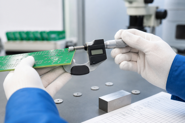
Component sourcing: 2 pin PCB connector sourcing, alternative review and BOM matching.
SMT and through-hole assembly: Suitable soldering process for different connector types.
Cable and mating check: Plug, crimp terminal and connector fit verification.
Testing support: Continuity, polarity, functional and load testing.
Quality control: IPC-based workmanship inspection and project-specific test plans.
Global delivery: China source factory production with overseas shipment.
EBest is a China PCB and PCBA source factory, not an overseas warehouse or local branch. The value is direct manufacturing, custom assembly, controlled quality, flexible OEM/ODM support and global supply.
FAQs About 2 Pin PCB Connectors
Q1: Can a 2 pin PCB connector be used with battery packs? A1: Yes. A 2 pin PCB connector is commonly used for battery positive and negative lines. However, battery circuits should use keyed housing, clear polarity marks and enough current margin. For rechargeable products, the connector, wire gauge and PCB copper path should also be checked under real charging and discharging load.
Q2: What is the difference between male and female 2 pin PCB connectors? A2: A male connector usually has exposed pins, while a female connector uses receptacle contacts. In many cable assemblies, the PCB side may be male and the cable side may be female. The final choice depends on safety, mating direction and product structure. For power input, exposed live pins should be avoided when possible.
Q3: Is a locking 2 pin PCB connector better than a friction-fit type? A3: A locking type is better when the cable may face vibration, movement or repeated handling. A friction-fit connector is simpler and often cheaper, but it may loosen more easily. For motors, fans, industrial modules and mobile devices, positive locking improves connection reliability and reduces field failure risk.
Q4: Can I use a 2 pin PCB connector for AC power? A4: Yes, but only if the connector has the correct voltage rating, current rating, insulation distance and flame-retardant material. Many small two-position connectors are only suitable for low-voltage DC. For AC input, PCB creepage, clearance and safety requirements must be checked carefully before production approval.
Q5: Why does a 2 pin PCB connector become hot? A5: Heat is usually caused by excessive current, poor mating, weak crimping, thin PCB copper, small pad area or oxidized contacts. The full current path should be reviewed, not only the connector datasheet. Check wire gauge, terminal contact, solder joint, trace width and temperature rise under real load.
Q6: What is a pluggable 2 pin PCB connector? A6: A pluggable type allows the cable or terminal plug to be removed from the PCB header. It is common in industrial controls, power modules and maintenance-friendly devices. This design makes wiring easier during installation and service. However, the mating plug, pitch and locking method must match exactly.
Q7: Can a 2 pin PCB connector be waterproof? A7: A normal PCB connector is not waterproof by default. Waterproof performance requires sealed housing, gasket, molded cable or protected enclosure design. For outdoor lighting, marine electronics or humid environments, check IP rating, connector sealing, conformal coating and enclosure protection together instead of relying on the connector alone.
Q8: What wire gauge should match a 2 pin PCB wire connector? A8: The wire gauge must match the connector terminal range. If the wire is too small, clamping may be loose. If it is too large, the terminal may deform or fail to insert. Always confirm AWG range, strip length and crimp terminal specification before cable harness assembly.
Q9: Can I replace a screw terminal with a JST 2 pin PCB connector? A9: Yes, but only when current, voltage, wire gauge and installation conditions are suitable. A screw terminal is better for field wiring and larger wires. A JST-style connector is better for compact products and controlled cable harness assembly. For high current, check temperature rise and retention force first.
Q10: What causes a 2 pin PCB connector to fall off the board? A10: Common causes include weak SMT pad design, cable pulling, insufficient solder, wrong footprint, poor wetting and no mechanical support. For connectors exposed to stress, use through-hole pins, anchor tabs, support posts or strain relief. The PCB design should consider real cable force during use.
Q11: Is a 2 pin PCB edge connector the same as a normal header? A11: No. A 2 pin PCB edge connector uses the PCB edge or plated contact area as part of the connection interface. A normal header is a separate component soldered to pads or holes. Edge connectors save height, but they require accurate board edge design and compatible mating slots.
Q12: What documents should buyers provide for connector assembly quotation? A12: Buyers should provide Gerber files, BOM, connector part number, datasheet, assembly drawing, current requirement, mating plug details and order quantity. If the exact connector is not confirmed, provide pitch, mounting style, wire gauge and target current. These details help prevent wrong footprint and wrong sourcing.
Q13: Can EBest source alternative 2 pin PCB connectors? A13: Yes. EBest can review alternatives based on pitch, footprint, current rating, height, mating plug, availability and cost. Before replacement, the alternative connector should be checked against PCB layout and cable harness. For mass production, sample approval and functional testing should be completed before batch use.
Q14: How can buyers reduce connector shortage risk? A14: Buyers can reduce shortage risk by selecting common connector series, approving second sources early and avoiding rare parts with long lead times. For repeat orders, keeping the same connector family across related products can simplify sourcing. Before PCB assembly starts, confirm stock, lead time and approved alternatives.
Q15: What sample checks are recommended before mass production? A15: Before mass production, check connector fit, mating plug insertion, polarity, solder joint quality, cable pull strength, enclosure clearance and functional performance. For a 2 pin PCB power connector, run a real load test and check temperature rise. Sample approval should confirm both electrical and mechanical reliability.
Conclusion
A reliable 2 pin PCB connector should be selected by current rating, pitch, wire gauge, mounting style, material, PCB layout, soldering process and final testing requirements. For low-current signal use, stable mating and clear polarity are important. For battery input, LED drivers, motor control and industrial wiring, current margin, copper design and mechanical support are more critical.
For procurement, do not choose a connector only by appearance or unit price. A qualified PCB assembly supplier should review the connector, footprint, mating cable, assembly process and test plan together before production. EBest Circuit is a China source PCB and PCBA manufacturer supporting custom connector assembly, OEM/ODM projects, bulk production and global delivery. Send your Gerber files, BOM and connector requirements to sales@bestpcbs.com for a fast quotation.

For professional electronics buyers, populated printed circuit boards are more than assembled boards with components soldered on them. They are production-ready PCBAs that must meet design intent, component sourcing requirements, soldering reliability, test standards, delivery schedules, and final product performance. A project may start with a Gerber file and BOM, but turning it into a stable PCBA requires engineering review, PCB fabrication control, component verification, SMT assembly, through-hole soldering, inspection, testing, and production documentation.
Best Technology provides custom populated printed circuit boards services from prototype to production. We support bare PCB manufacturing, component sourcing, PCB SMT assembly, DIP assembly, mixed assembly, AOI inspection, X-ray inspection, functional testing, packaging, and global delivery. For prototypes, low-volume builds, and batch production, our team helps customers reduce handover risks and keep the PCB-to-PCBA process under one coordinated system. For project review or quotation, please send your Gerber files, BOM, pick-and-place file, assembly drawing, quantity, and testing requirements to sales@bestpcbs.com.
What Are Populated Printed Circuit Boards?
Populated printed circuit boards are PCBs that already have electronic components mounted and soldered onto the board. These components may include resistors, capacitors, ICs, connectors, relays, LEDs, sensors, transformers, switches, and other parts required by the product design.
In practical engineering and purchasing communication, populated printed circuit boards are also called:
Populated PCBs
Assembled PCBs
PCBAs
PCB with components
Printed circuit board assemblies
A bare PCB is only the foundation. It contains copper traces, pads, vias, solder mask, silkscreen, and surface finish, but it cannot perform the final electronic function alone. After components are installed and soldered, the board becomes a functional electronic assembly.
For professional customers, the key difference is not only terminology. The real difference is responsibility.
Item
Bare PCB
Populated PCB / PCBA
Component status
No components
Components mounted and soldered
Function
Cannot work alone
Can be tested and used in a device
Supplier scope
PCB fabrication only
PCB fabrication + assembly + inspection
Main risk
Material, stack-up, copper, drilling
BOM, soldering, polarity, testing, function
Buyer focus
Board quality
Full assembly reliability
A populated PCB project usually involves more coordination than a bare PCB order. The supplier needs to understand the PCB design, BOM accuracy, part availability, assembly process, inspection requirements, and final test method. This is why many professional buyers prefer a manufacturer that can manage both PCB fabrication and PCBA assembly.
Custom Populated PCB Assembly Services We Offer
Best Technology provides custom populated PCB assembly services for customers who need more than basic component soldering. Our service is designed for projects that require controlled manufacturing, flexible order quantities, engineering communication, and reliable delivery.
Our populated PCB services include the following major areas:
1. Bare PCB Fabrication
We can manufacture the bare circuit board before assembly, which helps reduce mismatch between PCB production and assembly requirements.
We support:
FR4 PCB
HDI PCB
Rigid-flex PCB
Flexible PCB
Aluminum PCB
Copper base PCB
Ceramic PCB
Heavy copper PCB
High Tg PCB
Impedance control PCB
Multilayer PCB
Special surface finish PCB
This is useful when your populated circuit boards require special materials, controlled impedance, high-current design, thermal management, or compact routing.
2. SMT Assembly
SMT assembly is used for surface-mount components and high-density PCB designs. It is suitable for compact boards, automated production, and modern electronic products.
We support:
Resistors and capacitors
Diodes and LEDs
ICs and controllers
QFN, QFP, SOP, SOT packages
BGA assembly
Fine-pitch components
Sensors and communication modules
Small passive components
For dense PCBA projects, SMT process control is critical. Solder paste printing, placement accuracy, reflow profile, and AOI inspection all affect final board reliability.
3. Through-Hole Assembly
Some populated PCBs still require through-hole components because of mechanical strength, high current, or connector durability.
Common through-hole components include:
Pin headers
Terminal blocks
Transformers
Relays
Large capacitors
Connectors
Switches
Power components
Mechanical support parts
Through-hole assembly may involve manual soldering, wave soldering, or selective soldering, depending on the design and production quantity.
4. Mixed Assembly
Many custom populated printed circuit boards use both SMT and through-hole parts. These projects need a clear process route because the board may pass through several assembly stages.
A typical mixed assembly project may include:
Solder paste printing
SMT placement
Reflow soldering
AOI inspection
Through-hole insertion
Wave soldering or manual soldering
Final inspection
Functional testing
Mixed assembly is common in industrial control boards, power supply boards, LED driver boards, communication modules, and automotive electronic modules.
5. Component Sourcing
For turnkey populated PCB projects, we can source components according to the customer’s BOM.
Our sourcing support includes:
Manufacturer part number checking
Package verification
Quantity confirmation
Availability review
Lead time checking
Alternative part suggestion
Obsolete component warning
Customer approval before substitution
Component sourcing is one of the most important parts of populated PCB production. A wrong package, wrong voltage rating, wrong tolerance, or unapproved substitute can create serious production issues. That is why BOM review is completed before assembly starts.
6. Inspection and Testing
Inspection and testing are not optional details. They are part of the production strategy.
Depending on project requirements, we can support:
Visual inspection
AOI inspection
X-ray inspection
First article inspection
ICT
Flying probe testing
Functional testing
Customer-specific test procedure
Final quality report
For BGA, QFN, and other hidden-joint packages, X-ray inspection is especially useful because the solder joints cannot be fully checked by visual inspection alone.
7. Packaging and Delivery
Finished populated PCBs need proper packaging to avoid damage during transportation.
Packaging can be arranged based on:
Component height
Board size
Connector position
Moisture sensitivity
ESD requirements
Quantity per carton
Customer labeling requirements
Export shipping method
For professional customers, good packaging is part of quality control. A board that passes testing still needs to arrive safely.
How We Build Populated PCBs from Bare Boards?
A reliable populated PCB is not created by one assembly step. It is built through a controlled production chain. At Best Technology, the process starts with engineering review and continues through PCB fabrication, component preparation, assembly, inspection, testing, and shipment.
The typical build process includes:
1. Engineering File Review
Before production, our engineering team reviews the files provided by the customer.
We check:
Gerber file completeness
PCB stack-up and material notes
BOM accuracy
Component package matching
Polarity marks
Pick-and-place coordinates
Assembly drawing notes
Special soldering requirements
Testing requirements
This step helps identify possible problems before they enter production. For example, a mismatch between BOM package and PCB footprint can delay assembly or cause wrong placement. A missing polarity mark can create functional failure. A connector direction issue can affect final enclosure installation.
2. PCB Fabrication Preparation
Once the PCB data is confirmed, the bare board is manufactured according to the project specification.
Key points include:
Material selection
Copper thickness
Board thickness
Layer count
Surface finish
Solder mask color
Silkscreen clarity
Hole tolerance
Impedance control, if required
Panelization for assembly
For populated printed circuit boards, PCB fabrication must consider later assembly needs. Pad quality, surface finish, solder mask registration, and panel design all affect SMT performance.
3. Component and BOM Verification
Before assembly, components are checked against the BOM.
We review:
Part number
Package type
Quantity
Polarity
Moisture sensitivity
Storage condition
Substitute approval
Customer-supplied parts, if any
This is especially important for turnkey and hybrid projects. When parts are sourced by the manufacturer, clear approval rules help prevent wrong substitutions.
4. SMT Assembly
The SMT PCB assembly process includes solder paste printing, component placement, and reflow soldering.
Key control points include:
Stencil design
Solder paste volume
Printing alignment
Placement accuracy
Reflow temperature profile
Component shift control
Tombstone prevention
Solder bridge prevention
For fine-pitch ICs, BGA, QFN, small passive parts, LEDs, and thermal pads, SMT process control directly affects production yield.
5. Through-Hole and Manual Assembly
If the board includes through-hole or mechanical components, they are assembled after SMT or according to the planned route.
This stage may include:
Manual insertion
Manual soldering
Wave soldering
Selective soldering
Connector alignment check
Mechanical fit check
Professional handling is important because through-hole parts often face mechanical stress during product installation.
6. Inspection and Testing
After assembly, populated PCBs are inspected and tested according to project needs.
Common inspection steps include:
AOI for SMT defects
X-ray for BGA and QFN solder joints
Visual inspection for connectors and through-hole parts
First article inspection for new projects
Functional testing based on customer test procedure
The purpose is not only to find defects. It is to confirm that the board is ready for customer validation or final use.
Turnkey and Consigned Options for Populated PCB Projects
Professional customers often have different supply chain strategies. Some prefer a complete turnkey service. Others want to provide key components themselves. Best Technology supports both options.
Option 1: Turnkey Populated PCB Service
In turnkey service, we manage the full production chain.
This can include:
PCB fabrication
Component sourcing
BOM review
SMT assembly
Through-hole assembly
Inspection
Testing
Packaging
Shipment
Turnkey service is suitable for customers who want fewer suppliers and smoother coordination.
It is especially useful when:
The BOM contains many standard parts
The customer wants to reduce purchasing workload
The project needs faster supplier communication
PCB and assembly should be coordinated together
The customer needs prototype-to-production support
The main advantage is efficiency. Instead of managing PCB supplier, component supplier, assembly factory, and testing partner separately, the customer can work with one manufacturing team.
Option 2: Consigned Assembly
In consigned assembly, the customer provides all or part of the components. We handle the PCB fabrication and assembly work based on the provided materials and production files.
Consigned assembly is suitable when:
The customer already has approved components
Some ICs are customer-controlled
Certain parts are expensive or difficult to source
The customer has existing supplier agreements
Components require programming before assembly
The customer wants strict control over key parts
Before production, we check the received components and confirm quantity, packaging, and condition.
Option 3: Hybrid Assembly
Many projects use a hybrid model. The customer provides key ICs, programmed parts, or special components, while we source standard passive components, connectors, and common parts.
This option gives customers both control and flexibility.
Service Model
Best For
Customer Provides
Best Technology Handles
Turnkey
Full project outsourcing
Design files and BOM
PCB, parts, assembly, testing
Consigned
Customer-controlled components
Components and files
Assembly and inspection
Hybrid
Mixed sourcing strategy
Key parts
Common parts, PCB, assembly
The right choice depends on cost, lead time, component risk, and internal purchasing policy.
Prototype Populated PCB Services for Design Validation
Prototype populated PCBs are used to verify the design before batch production. This stage is important because it helps customers find design, assembly, sourcing, and testing issues early.
For professional projects, prototype production is not simply “making a few samples.” It is a risk-control step before larger investment.
What Prototype Builds Help Validate
A prototype populated PCB can help check:
Circuit function Confirm whether the board performs as designed.
Component package matching Check whether BOM parts match PCB footprints.
Polarity and orientation Verify LEDs, diodes, ICs, electrolytic capacitors, and connectors.
Mechanical fit Confirm connector direction, component height, enclosure fit, and mounting holes.
Thermal behavior Check whether heat-generating components need layout or material adjustment.
Testing method Confirm how the board should be powered, measured, programmed, and validated.
How We Support Prototype Projects
For prototype populated printed circuit boards, we can support:
Small-batch PCB fabrication
Quick SMT assembly
Through-hole assembly
Engineering file review
DFM and DFA feedback
First article inspection
Functional testing support
Production notes for next batch
The prototype stage also helps prepare for pilot production. Once the prototype is approved, we can improve stencil design, assembly route, test plan, packaging method, and production documentation for repeat orders.
This is valuable for R&D teams, startups, OEM brands, hardware companies, industrial product developers, and customers preparing for mass production.
Quality Control for Populated Printed Circuit Boards
Quality control for populated printed circuit boards must cover the full process. A board can fail because of PCB defects, wrong components, poor soldering, incorrect polarity, weak connectors, insufficient testing, or packaging damage. A reliable manufacturer must control each stage.
At Best Technology, quality control is divided into several layers.
1. PCB Quality Control
Before assembly, the bare PCB must meet the design specification.
We check:
Board dimension
Hole quality
Surface finish
Solder mask
Silkscreen
Pad condition
Warpage
Panel quality
Electrical performance, if required
PCB quality affects assembly quality. Poor pad finish or board warpage can create soldering issues.
2. Component Quality Control
Components are checked before production.
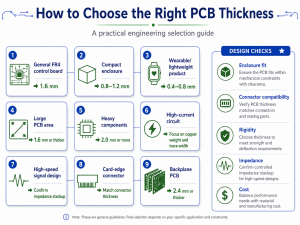
Important checks include:
Correct part number
Correct package
Correct quantity
Moisture sensitivity
Visible damage
Polarity
Storage condition
Customer approval for substitutes
This step reduces the risk of wrong assembly and functional failure.
3. SMT Process Control
During SMT assembly, solder paste printing and placement accuracy are controlled carefully.
Key inspection points include:
Solder paste coverage
Component alignment
Missing parts
Polarity direction
Solder bridges
Tombstoning
Fine-pitch solder quality
AOI inspection is widely used after reflow soldering.
4. X-Ray Inspection for Hidden Solder Joints
For BGA, QFN, LGA, and some bottom-terminated components, solder joints are hidden under the package. X-ray inspection helps check:
Solder ball alignment
Bridging
Voiding
Open joints
Insufficient solder
Short circuits
This is important for high-density and high-reliability populated PCBs.
5. Functional Testing
Functional testing checks whether the assembled board works according to the customer’s requirement.
Testing may include:
Power-on test
Voltage and current check
LED indicator check
Signal input/output test
Communication test
Firmware or programming check
Load test
Customer test fixture operation
For complex products, the customer may provide a test procedure or test fixture. We can follow the approved method during production.
6. Final Inspection and Packaging Check
Before shipment, final inspection confirms:
Board appearance
Labeling
Quantity
Packaging method
Connector protection
ESD protection
Carton information
Shipment documents
This final step helps ensure that the boards arrive in usable condition.
Custom Populated PCB Types We Can Build
Different electronic products need different PCB structures. Best Technology supports various populated PCB types for prototype, low-volume, and batch production projects.
1. FR4 Populated PCBs
FR4 populated PCBs are widely used in consumer electronics, industrial control, communication devices, power modules, and general electronic products.
They are suitable for:
Control boards
Sensor boards
Communication modules
Smart home devices
Industrial controllers
General PCBA projects
FR4 offers a practical balance of cost, mechanical strength, and electrical performance.
2. HDI Populated PCBs
HDI populated PCBs are used when the product needs compact size and high routing density.
They are suitable for:
Portable electronics
Communication devices
Medical instruments
High-density control modules
Products using small BGAs or fine-pitch ICs
HDI projects require strong coordination between PCB fabrication and assembly because pad size, via structure, and component density are more demanding.
3. Rigid-Flex Populated PCBs
Rigid-flex populated PCBs combine rigid board areas and flexible circuits. They are useful when the product has limited space or needs folding installation.
They are suitable for:
Wearable devices
Medical electronics
Compact instruments
Camera modules
Aerospace electronics
Complex mechanical designs
Rigid-flex assembly needs careful handling because the flexible area can be damaged by stress or incorrect fixture design.
4. Aluminum Populated PCBs
Aluminum populated PCBs are used when thermal dissipation is important.
They are suitable for:
LED lighting
Power modules
Motor control
Automotive lighting
High-power driver boards
The metal base helps move heat away from components, improving thermal stability.
5. Ceramic Populated PCBs
Ceramic populated PCBs are used in high-power, high-temperature, high-frequency, and high-reliability applications.
Common ceramic materials include:
Alumina
Aluminum nitride
Silicon nitride
They are suitable for:
Power electronics
Laser modules
Medical devices
RF applications
EV power modules
High-thermal-demand products
Ceramic PCB assembly requires proper process control because the substrate and metallization structure differ from standard FR4 boards.
6. Heavy Copper Populated PCBs
Heavy copper populated PCBs are designed for higher current applications.
They are suitable for:
Battery systems
Power control boards
Industrial equipment
Energy storage systems
High-current modules
Heavy copper boards need careful thermal and soldering consideration during assembly.
7. Impedance Control Populated PCBs
Impedance control populated PCBs are used for high-speed and signal-sensitive applications.
They are suitable for:
RF products
Communication equipment
High-speed digital modules
Data transmission boards
Signal control devices
These projects require controlled stack-up, trace width, dielectric thickness, and manufacturing tolerance.
Files Needed for a Populated PCB Quote
A clear quote depends on clear technical files. When customers request a populated PCB quote, incomplete information may cause delays or inaccurate pricing. To help us quote quickly and correctly, please prepare the following files.
1. Gerber Files
Gerber files define the PCB manufacturing data.
They should include:
Copper layers
Solder mask
Silkscreen
Drill data
Board outline
Surface finish notes
Panel information, if available
For special boards, please also provide material, thickness, copper weight, impedance, and stack-up requirements.
2. BOM
The BOM is one of the most important files for populated printed circuit boards.
A complete BOM should include:
Reference designator
Component value
Package
Manufacturer part number
Brand or manufacturer
Quantity
Description
Approved alternatives, if allowed
Do-not-substitute parts, if any
A clear BOM helps avoid wrong components and speeds up sourcing.
3. Pick-and-Place File
The pick-and-place file is also called a centroid file or CPL file.
It should include:
Component coordinates
Rotation
Placement side
Reference designators
This file is used for SMT programming.
4. Assembly Drawing
The assembly drawing helps confirm component orientation and mechanical details.
It may include:
Polarity marks
Connector direction
Component height notes
Manual soldering notes
Mechanical installation notes
Special assembly instructions
For complex boards, a 3D file is also helpful.
5. Testing Requirements
If functional testing is needed, please provide a clear test method.
Useful information includes:
Input voltage
Output requirement
Current limit
Signal requirement
Firmware or programming notes
Test fixture information
Pass/fail criteria
Test report format
6. Quantity and Lead Time
Please provide the target quantity and expected delivery time.
For example:
Prototype quantity
Pilot run quantity
Batch production quantity
Annual demand estimate
Urgent delivery requirement
This helps us plan material sourcing, production scheduling, and cost calculation.
Quote File Checklist
File / Information
Why It Matters
Gerber files
PCB fabrication
BOM
Component sourcing and cost
Pick-and-place file
SMT programming
Assembly drawing
Orientation and assembly details
Testing requirement
Functional verification
Quantity
Pricing and scheduling
Lead time
Production planning
Packaging notes
Shipment protection
For quotation, you can send these files to sales@bestpcbs.com.
Populated PCB Case Study: Prototype to Batch Production
This case involved a custom 6-layer heavy copper populated PCB project. The customer required strict control over copper thickness, board marking, testing, packaging, and shipment documentation before production release.
Project Specifications
Board type: 6-layer PCB
Material: FR4 IT180
Inner copper: 5 oz
Finished outer copper: 6 oz
Board thickness: 2.0828 mm / 0.082 inch, ±10%
Solder mask / silkscreen: Green solder mask, white silkscreen
Surface finish: ENIG, Au 3u”
Marking: Customer logo, YYWW date code, and RoHS label
Testing: 100% AOI and flying probe test before shipment
Reports: Shipment report required with delivery
Special requirement: Robber copper / plating thieving pattern, referring to B16P210543A0
Delivery: Single-unit boards according to customer data
Pre-production: Production files must be sent to the customer for confirmation
EQ item: Ls and Rd / DCR test values need customer confirmation
Key Engineering Controls
The main challenge was the heavy copper structure. With 5 oz inner copper and 6 oz finished outer copper, the project required careful control of plating uniformity, etching compensation, solder mask coverage, and final board thickness.
The customer also required clear product traceability. The company logo, YYWW production code, and RoHS label had to be printed clearly and placed where they would not be blocked by components, pads, or other board features.
Before production, our team reviewed the customer files and confirmed the production data. The robber copper pattern was added according to the referenced method to support more uniform copper plating. For unclear Ls and Rd / DCR testing values, EQ was raised before manufacturing.
Inspection and Shipment Requirements
Before shipment, the boards required:
100% AOI inspection
100% flying probe testing
Clear RoHS and date-code marking
Shipment report provided with goods
Packaging according to customer instructions
The packaging requirement was also important because heavy copper boards are thicker and heavier than standard PCBs. Proper packaging helped protect the ENIG surface, board edges, silkscreen labels, and shipment traceability.
Case Value
This case shows how a professional populated PCB project requires more than assembly. For heavy copper populated printed circuit boards, early engineering confirmation is essential. Copper thickness, board thickness, logo marking, RoHS label position, test reports, packaging, and EQ items must be confirmed before production.
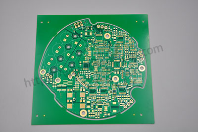
By reviewing the production data in advance, applying the required copper balancing pattern, and completing 100% AOI plus flying probe testing, the project could move from prototype confirmation to batch delivery with better process control.
FAQs About Populated Printed Circuit Boards
Q1. Are populated printed circuit boards the same as PCBA? Yes. In most manufacturing and purchasing situations, populated printed circuit boards and PCBA refer to the same type of product: a PCB with components mounted and soldered onto it.
Q2. Can Best Technology provide both PCB fabrication and assembly? Yes. We can manufacture the bare PCB and complete the assembly process. This one-stop service helps reduce communication between separate suppliers.
Q3. Do you support turnkey populated PCB assembly? Yes. We can support PCB fabrication, component sourcing, SMT assembly, through-hole assembly, inspection, testing, packaging, and shipment.
Q4. Can customers provide their own components? Yes. We support consigned assembly. Customers can provide all components or only key parts. We can also source the remaining components if needed.
Q5. What files are needed for a populated PCB quote? The basic files include Gerber files, BOM, pick-and-place file, assembly drawing, quantity, and testing requirements.
Q6. Can you assemble BGA, QFN, and fine-pitch components? Yes. We support BGA, QFN, QFP, fine-pitch ICs, SMD passives, connectors, LEDs, and mixed assembly projects.
Q7. Can populated PCBs be tested before shipment? Yes. We can provide AOI, X-ray inspection, visual inspection, ICT, functional testing, and customer-specific test procedures based on project needs.
Q8. Do you support prototype populated PCBs? Yes. We support prototype assembly for design validation, engineering review, functional testing, and preparation before batch production.
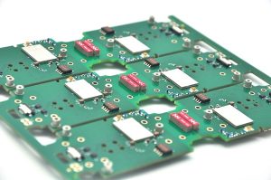
Q9. What industries use populated printed circuit boards? They are used in industrial control, medical electronics, automotive electronics, communication equipment, LED lighting, smart devices, power electronics, and consumer products.
Q10. How do I start a populated PCB project with Best Technology? You can send your Gerber files, BOM, pick-and-place file, assembly drawing, quantity, and testing requirements to sales@bestpcbs.com. Our team will review the project and provide a quotation.
All in all, custom populated printed circuit boards require more than component placement. A successful PCBA project depends on accurate engineering files, reliable PCB fabrication, correct component sourcing, controlled SMT assembly, stable soldering, proper inspection, functional testing, and safe packaging.
For professional buyers, the right supplier should not only build the board. The supplier should help reduce project risk from prototype to production. That includes reviewing the BOM, checking component packages, confirming assembly details, supporting turnkey or consigned options, and preparing the project for repeatable batch manufacturing.
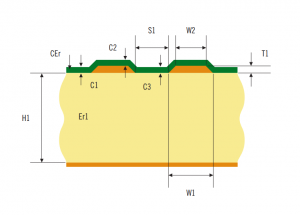
Best Technology provides custom populated printed circuit boards services for prototypes, small batches, and production orders. We support PCB fabrication, SMT assembly, through-hole assembly, component sourcing, AOI inspection, X-ray inspection, functional testing, and global delivery.
If you are preparing a populated PCB project, please send your Gerber files, BOM, pick-and-place file, assembly drawing, quantity, and testing requirements to sales@bestpcbs.com. Our engineering and sales team will review your files and provide a practical quotation for your next build.
This website uses cookies to enhance your experience, remember your preferences, and help us understand how visitors use our site. You can accept all cookies, reject non-essential cookies, or manage your settings.
This website uses cookies to improve your experience while you navigate through the website. Out of these cookies, the cookies that are categorized as necessary are stored on your browser as they are essential for the working of basic functionalities of the website. We also use third-party cookies that help us analyze and understand how you use this website. These cookies will be stored in your browser only with your consent. You also have the option to opt-out of these cookies. But opting out of some of these cookies may have an effect on your browsing experience.
Necessary cookies are absolutely essential for the website to function properly. These cookies ensure basic functionalities and security features of the website, anonymously.
Cookie
Duration
Description
cookielawinfo-checkbox-analytics
11 months
This cookie is set by GDPR Cookie Consent plugin. The cookie is used to store the user consent for the cookies in the category "Analytics".


cookielawinfo-checkbox-functional
11 months
The cookie is set by GDPR cookie consent to record the user consent for the cookies in the category "Functional".
cookielawinfo-checkbox-necessary
11 months
This cookie is set by GDPR Cookie Consent plugin. The cookies is used to store the user consent for the cookies in the category "Necessary".
cookielawinfo-checkbox-others
11 months
This cookie is set by GDPR Cookie Consent plugin. The cookie is used to store the user consent for the cookies in the category "Other.
cookielawinfo-checkbox-performance
11 months
This cookie is set by GDPR Cookie Consent plugin. The cookie is used to store the user consent for the cookies in the category "Performance".
viewed_cookie_policy
11 months
The cookie is set by the GDPR Cookie Consent plugin and is used to store whether or not user has consented to the use of cookies. It does not store any personal data.
Functional cookies help to perform certain functionalities like sharing the content of the website on social media platforms, collect feedbacks, and other third-party features.
Performance cookies are used to understand and analyze the key performance indexes of the website which helps in delivering a better user experience for the visitors.
Analytical cookies are used to understand how visitors interact with the website. These cookies help provide information on metrics the number of visitors, bounce rate, traffic source, etc.
Advertisement cookies are used to provide visitors with relevant ads and marketing campaigns. These cookies track visitors across websites and collect information to provide customized ads.