PCB manufacturing PCB manufacturing
Home > Blog

BGA assembly

What Is PoP Package on Package?
Thursday, June 25th, 2026

PoP Package on Package is a stacked IC packaging method that places one package, usually memory, on top of another package, usually a logic processor, to save PCB area and shorten signal paths. This article explains how PoP works, what its structure looks like, how package on package PoP assembly is handled, and what engineers should know before using it in compact electronic products.

As electronic products become thinner, faster, and more functionally dense, many buyers face a familiar challenge: the PCB layout has less room, but the product still needs stronger computing power, larger memory, and stable manufacturing yield.

What problems do customers often face when a compact PCB design requires logic and memory in the same limited area?

  • PCB space disappears quickly. The processor, memory, power circuits, and RF sections compete for the same board area.
  • High-speed routing becomes crowded. Dense signal lines between the processor and memory may increase layout complexity.
  • Hidden solder joints are hard to inspect. BGA and PoP solder joints cannot be judged by visual inspection alone.
  • Warpage can create unstable defects. Fine-pitch packages may suffer from open joints or head-in-pillow defects during reflow.
  • Supplier communication becomes unclear. If the PoP stack, ball layout, and assembly process are not confirmed early, production risk increases.

A professional PCBA manufacturer reduces these risks by checking the package structure, SMT process, and inspection plan before mass production.

  • For limited PCB space, we review whether PoP can reduce component footprint and improve layout efficiency.
  • For crowded routing, we check ball pitch, escape routing, layer stack-up, and impedance requirements.
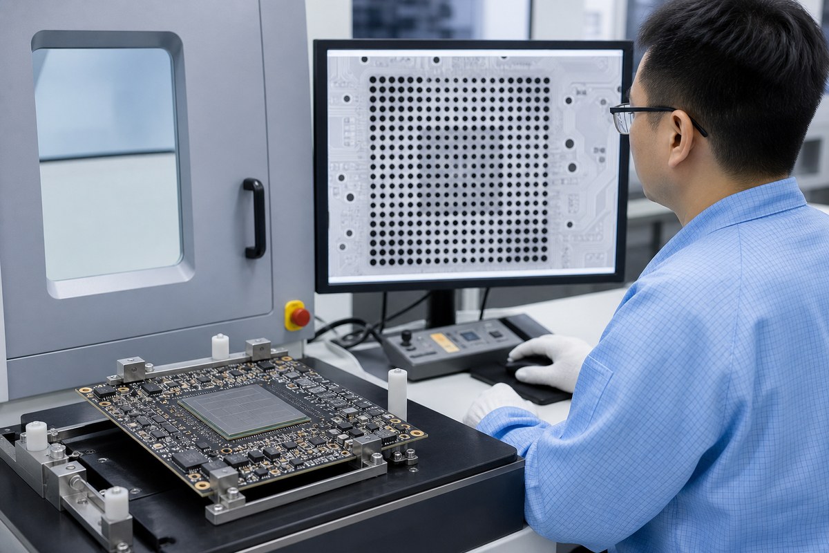
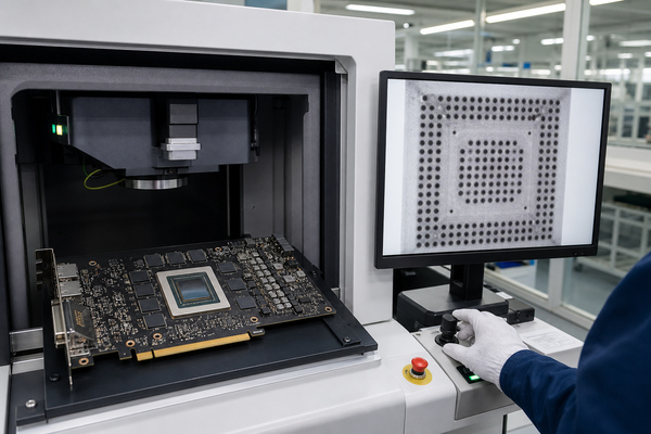
  • For hidden solder joints, we use X-ray inspection and process control for BGA and PoP assembly.
  • For warpage risk, we control baking, placement accuracy, flux or solder paste dipping, and reflow profiling.
  • For unclear specifications, we confirm datasheets, top and bottom package compatibility, test requirements, and production notes before assembly.

EBest Circuit (Best Technology) provides PCB manufacturing and PCBA assembly services for compact, high-density, and advanced electronic products. Our engineering team supports SMT assembly, BGA assembly, X-ray inspection, functional testing, and turnkey PCBA assembly services. If your project involves PoP Package on Package, BGA, fine-pitch components, or high-density PCB assembly, you can send your Gerber files, BOM, placement file, and assembly requirements to sales@bestpcbs.com for engineering review.

PoP Package on Package

What Is PoP Package on Package?

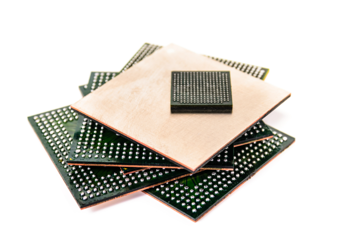
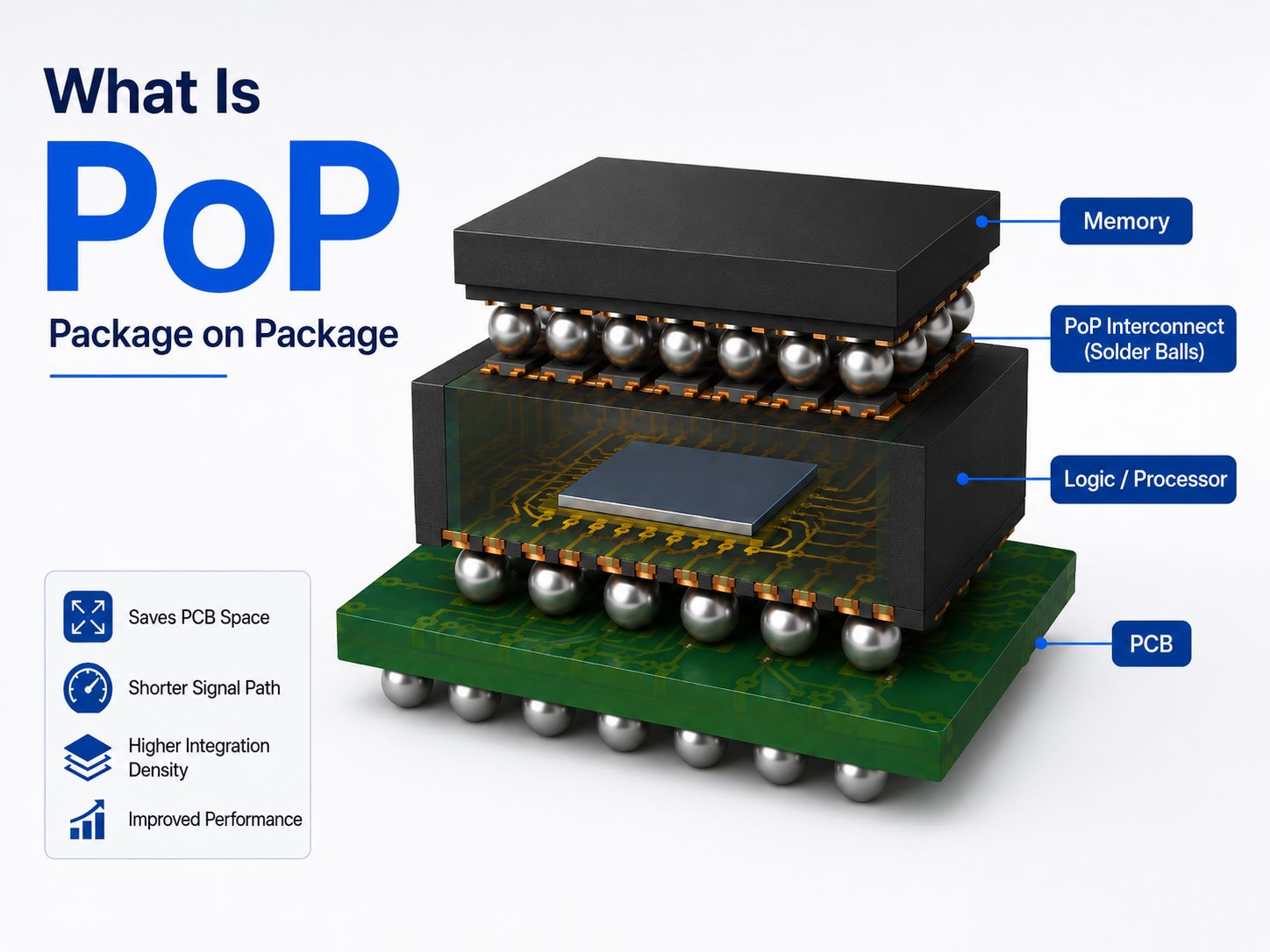
PoP Package on Package is a 3D IC packaging approach where two or more completed packages are vertically stacked. The most common combination is a bottom logic package and a top memory package. Instead of placing the processor and memory side by side on the PCB, PoP places them in a vertical structure.

In simple terms, PoP means “package stacked on package.”

A typical PoP stack looks like this:

LayerTypical DeviceMain Function
Top PackageLPDDR, NAND Flash, MemoryData storage
Bottom PackageApplication Processor, SoC, Logic ICComputing and control
PCBMain circuit boardElectrical connection and system support

This structure allows the designer to use the same PCB footprint for two functional blocks. For smartphones, wearable devices, compact modules, and portable electronics, this can be very valuable.

The main idea is simple:

Board area saving ≈ footprint of the top package if it were mounted separately − extra keep-out and routing margin

PoP does not remove all design complexity, but it gives engineers a practical way to increase system integration without enlarging the PCB. That is why engineers, buyers, and product developers often study PoP when they want to understand how compact electronics achieve higher performance in limited space.

In short, PoP Package on Package is not just a packaging name. It is a space-saving and performance-oriented structure used when logic and memory need to work closely together.

How Does Package on Package PoP Work?

Package on Package PoP works by connecting the top package to the bottom package through solder balls, while the bottom package connects to the PCB through its own solder balls. The upper and lower packages are designed to match each other mechanically and electrically.

The bottom package usually has two connection interfaces:

  • Bottom-side solder balls for connection to the PCB.
  • Top-side pads or exposed connection points for connection to the upper memory package.

The top package has solder balls on its bottom side. During assembly, these balls are aligned with the top-side pads of the bottom package. After reflow soldering, the top and bottom packages become one stacked structure.

A simplified connection path looks like this:

Connection PathPurpose
Top memory package to bottom logic packageData transfer
Bottom logic package to PCBSystem connection
PCB routing to other circuitsPower, control, RF, I/O

The most important feature is vertical interconnection. Traditional PCB design connects processor and memory through horizontal traces on the PCB. PoP shortens part of this path by stacking the packages vertically.

This brings several engineering benefits:

  • Shorter processor-to-memory connection
  • Smaller PCB footprint
  • Higher system packaging density
  • Flexible memory selection
  • Better use of limited board space

However, PoP also increases assembly sensitivity. The solder balls between the top and bottom packages are hidden, and the final solder quality depends on package coplanarity, placement accuracy, flux activity, solder volume, and reflow temperature control.

So, package on package PoP works through a matched vertical interconnect system. It saves space, but it also requires careful design and controlled SMT assembly.

What Is PoP Package on Package Assembly?

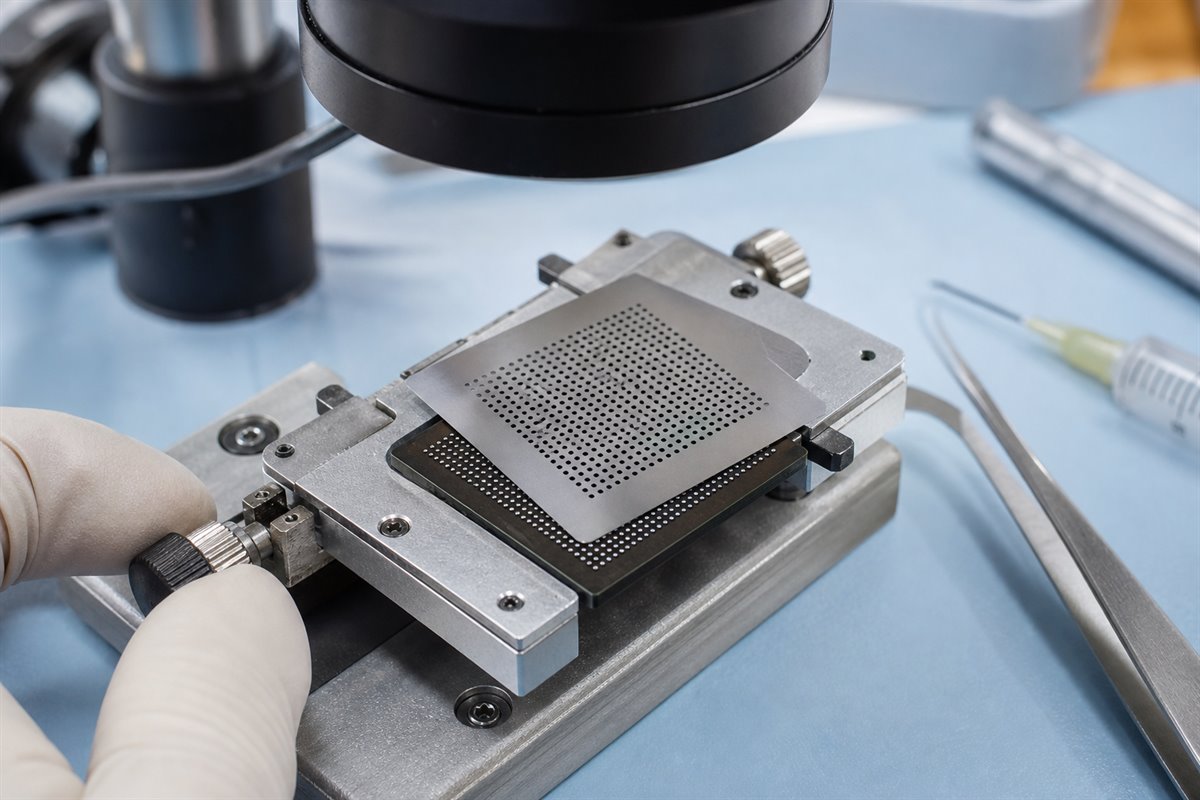
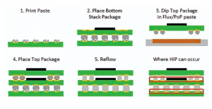
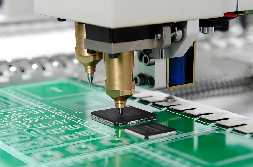
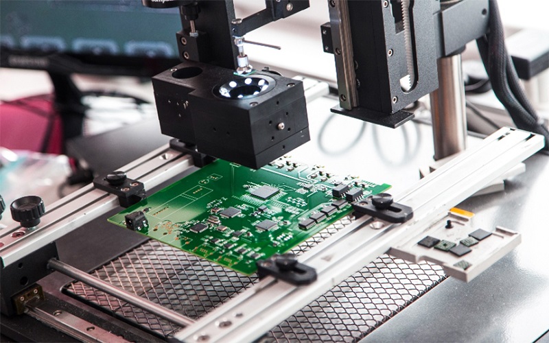
PoP Package on Package assembly is the SMT process used to mount the bottom package onto the PCB and then mount the top package onto the bottom package. It is closely related to the SMT PoP (Package on Package) process, which focuses on solder paste printing, component placement, flux or solder paste dipping, reflow soldering, and X-ray inspection.

In many PCBA factories, PoP assembly follows this general flow:

  • PCB preparation
    The PCB is checked for cleanliness, flatness, solder mask quality, and pad condition.
  • Solder paste printing
    Solder paste is printed onto the PCB pads for the bottom PoP component.
  • Bottom package placement
    The logic package or SoC is placed onto the PCB with high-precision SMT equipment.
  • Top package dipping
    The memory package is dipped into flux or a controlled solder paste layer.
  • Top package placement
    The top package is placed onto the bottom package with accurate alignment.
  • Reflow soldering
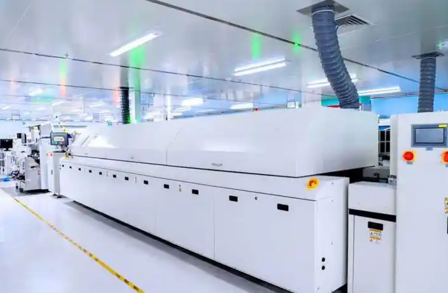
    The full PoP stack passes through the reflow oven to form solder joints.
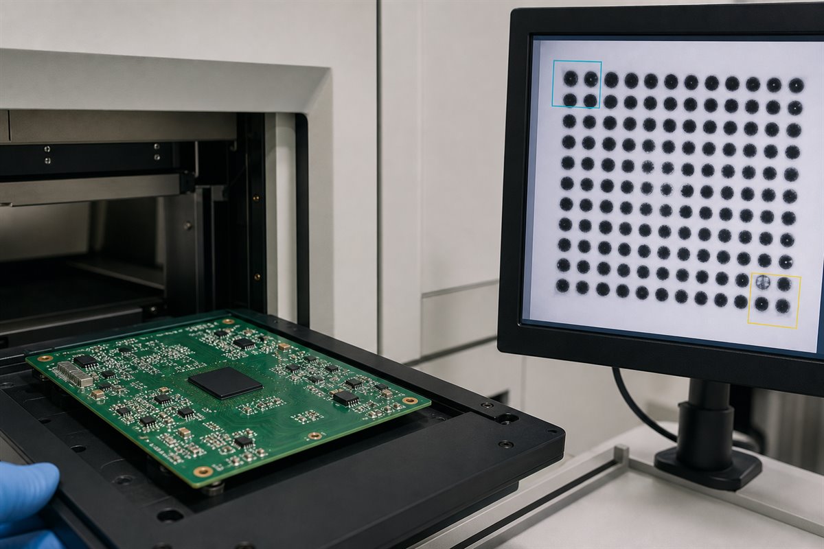
  • X-ray inspection
    Hidden joints are inspected to check solder quality, alignment, voiding, and bridging.
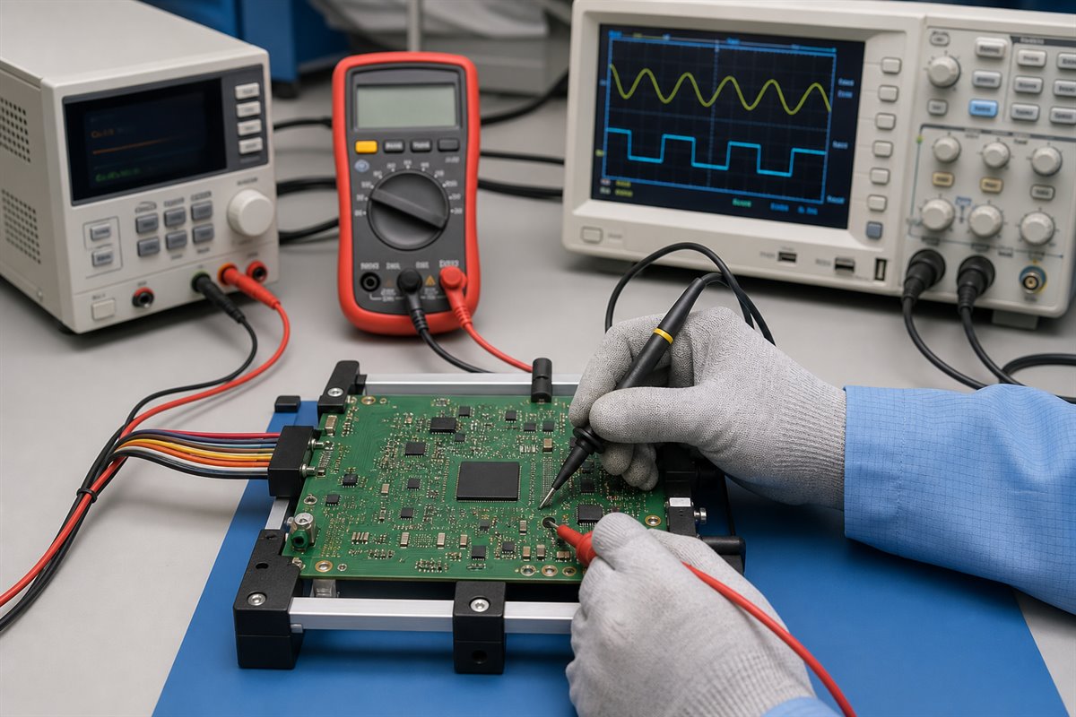
  • Electrical and functional testing
    The completed PCBA is tested based on the product requirement.

The key difference between ordinary BGA assembly and package on package pop assembly is that PoP has two soldering interfaces:

Assembly TypeSoldering Interface
Standard BGABGA to PCB
PoP AssemblyTop package to bottom package + bottom package to PCB

This means PoP assembly needs tighter process control than ordinary SMT mounting. The placement system must align both packages accurately, and the reflow profile must support the full stack without causing package warpage.

PoP Package on Package assembly is therefore not only about placing two packages together. It is a controlled PCBA process that combines fine-pitch SMT, BGA assembly, reflow profiling, and X-ray inspection.

What Is the Typical Structure of PoP Package on Package?

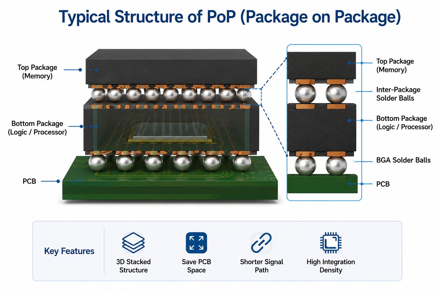
The typical structure of PoP Package on Package includes a bottom logic package, a top memory package, solder balls between the two packages, and solder balls between the bottom package and the PCB. This vertical structure is the foundation of PoP technology.

A common PoP structure includes:

Structure PartTypical Role
Top PackageMemory or storage
Inter-package Solder BallsConnection between top and bottom package
Bottom PackageProcessor, SoC, or logic IC
Bottom BGA BallsConnection to PCB
PCB PadsBoard-level electrical interface

The bottom package is usually larger because it often contains the logic IC, substrate routing, and top-side connection pads. The top package is commonly a memory device, but the exact structure depends on product design.

The structure can vary by application. Some designs use standard solder ball connected PoP. More advanced designs may use TMV, also known as through-mold via technology, to create a thinner and more compact package interface.
Common PoP structure types include:

  • Solder Ball Connected PoP
    The upper package connects to the lower package through solder balls.
  • TMV PoP
    Through-mold vias expose connection points through the mold compound for top package attachment.
  • Folded PoP
    Flexible circuit structures are folded to connect different package layers.
  • BVA PoP
    Bond Via Array technology supports fine-pitch vertical interconnects.
  • Memory Stacked PoP
    Multiple memory dies or memory packages are stacked for higher capacity.

The structure selected depends on package height, I/O count, cost target, signal performance, and manufacturing capability.

In short, the typical PoP Package on Package structure is built around one main purpose: placing logic and memory into a compact vertical package system while keeping each package manufacturable and testable.

PoP Package on Package

How Does the Ball Grid Work in PoP Package on Package?

The ball grid in PoP Package on Package provides the electrical and mechanical connection between the stacked packages and the PCB. In a standard BGA, the ball grid connects one package to the board. In PoP, the ball grid may connect both the bottom package to the PCB and the top package to the bottom package.

A PoP design may include two ball-grid levels:

Ball Grid PositionFunction
Top-to-bottom package ballsConnect memory to logic
Bottom-to-PCB ballsConnect logic package to PCB

The ball grid must support electrical performance, mechanical stability, and manufacturability. If the grid is too dense, PCB escape routing becomes difficult. If the ball pitch is too small, soldering and inspection become more demanding.

Important ball-grid factors include:

  • Ball pitch
  • Ball diameter
  • Pad size
  • Solder mask opening
  • Coplanarity
  • Warpage behavior
  • Reflow compatibility

In fine-pitch PoP packages, solder balls are often discussed in micron-level dimensions. Engineers may review ball diameter, standoff height, and solder joint reliability when checking package compatibility and assembly risk.

A useful way to think about PoP ball-grid risk is:

Smaller pitch + larger package size + higher warpage = higher assembly difficulty

This does not mean smaller pitch should be avoided. It means that process control must match the package requirement.

The ball grid is one of the most important parts of PoP Package on Package because it directly affects electrical connection, solder reliability, inspection difficulty, and PCB layout feasibility.

What Should Engineers Know About PoP Ball Layout?

PoP ball layout refers to the arrangement of solder balls and pads used to connect the top package, bottom package, and PCB. It affects routing density, signal integrity, solder reliability, and production yield.

For engineers and buyers, the practical question is clear: can the PCB and SMT PCB assembly process support this package safely?

Before production, engineers should check these key items:

  • Ball pitch
    Fine pitch improves density but increases routing and assembly difficulty.
  • Escape routing
    The PCB must have enough layer count and trace width/spacing capability to route signals out from the BGA area.
  • Pad design
    Pad size, solder mask defined pads, and non-solder mask defined pads must follow package recommendations.
  • Solder mask registration
    Misregistration can reduce solder joint quality or create bridging risk.
  • Power and ground ball placement
    Good power and ground distribution helps signal return paths and power integrity.
  • High-speed signal grouping
    Memory signals should be routed with controlled length, impedance, and return path planning.
  • Keep-out area
    The package area must leave enough space for assembly tolerance and inspection needs.

A compact comparison is shown below:

Design ItemWhy It Matters
Ball PitchControls density and difficulty
Pad DesignAffects solder quality
Escape RoutingDecides PCB layer need
Power/Ground BallsSupports stability
Warpage MarginReduces open-joint risk

A good PoP ball layout is not only a package drawing. It is a manufacturing guide. If the layout is not reviewed before PCB fabrication, problems may appear during PCB SMT assembly, X-ray inspection, or functional testing.

In short, PoP ball layout connects packaging design with real PCBA manufacturability.

How Does SMT Support High-Density PoP Package-on-Package Assembly?

SMT supports high-density PoP Package-on-Package assembly by providing accurate solder paste printing, fine-pitch placement, controlled dipping, stable reflow soldering, and X-ray inspection. Without a controlled SMT process, PoP packaging cannot deliver its expected space-saving and performance benefits.
Advanced PoP structures may use finer pitches, smaller solder joints, thinner package bodies, and TMV through-mold via technology. SMT assembly must be able to handle these features consistently.

The production side usually focuses on these process controls:

  • Stencil design
    Aperture size and solder paste volume must match the bottom package pad design.
  • Solder paste selection
    Paste type should support fine-pitch printing and stable reflow behavior.
  • Flux or solder paste dipping
    The top package may need controlled dipping to support inter-package soldering.
  • Placement accuracy
    Both top and bottom packages require precise alignment.
  • Reflow profile
    Temperature ramp, soak, peak temperature, and cooling rate must be controlled.
  • X-ray inspection
    Hidden solder joints must be inspected after reflow.
  • MSL control
    Moisture-sensitive packages may require dry storage or baking before assembly.

For high-density PoP assembly, the process window can be narrow. A small placement shift, uneven solder paste deposit, or poor reflow profile may create hidden defects.

Common defects include:

  • Head-in-pillow
  • Solder bridging
  • Open joints
  • Insufficient solder
  • Voids
  • Package warpage
  • Misalignment

The SMT process is therefore the bridge between the PoP package design and the final working PCBA. PoP Package on Package depends on strong packaging design, but it also depends on disciplined SMT execution.
What Is TMV PoP with Through-Mold Vias?

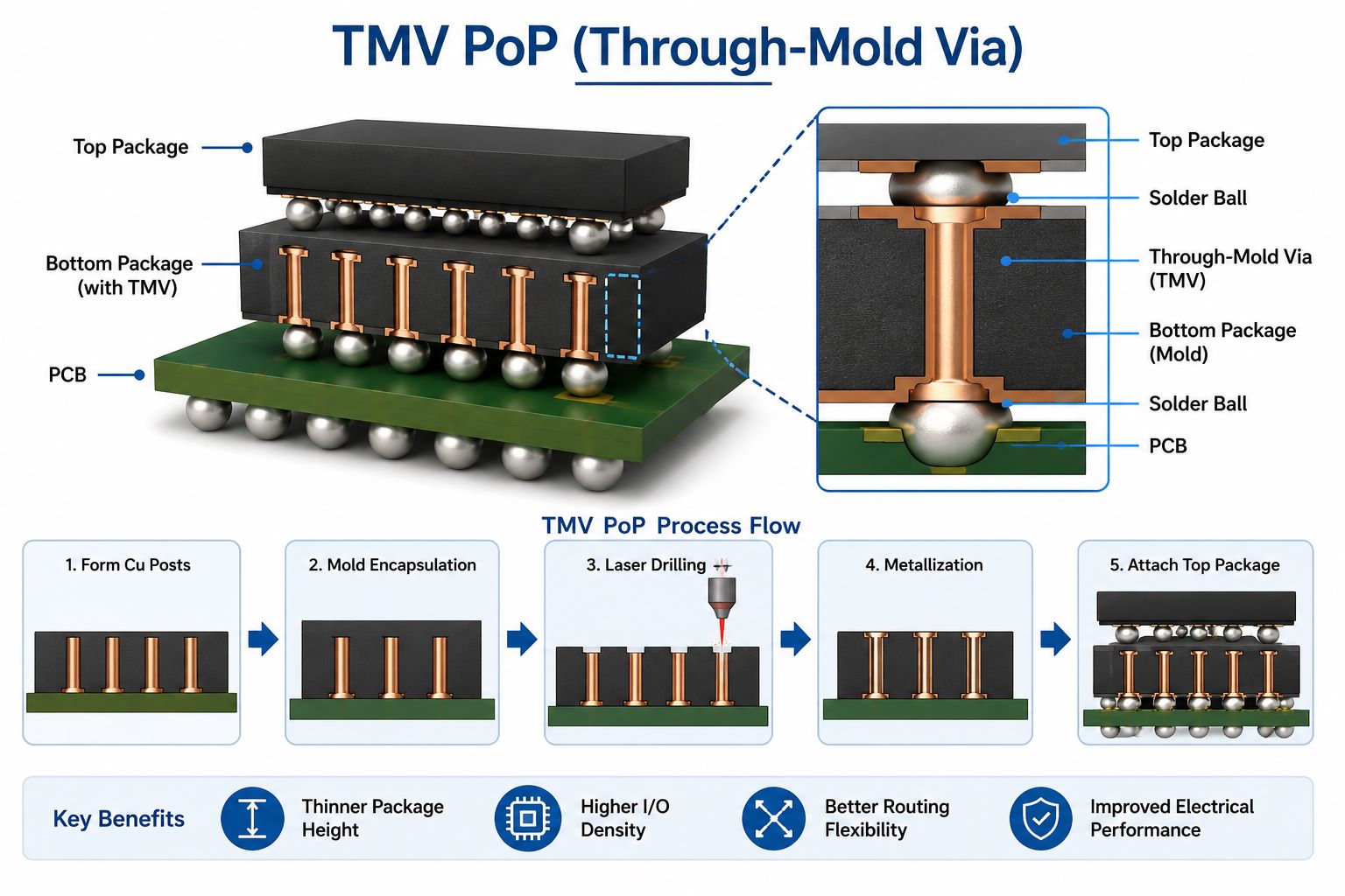
TMV PoP with through-mold vias is an advanced PoP structure where vertical connection paths are formed through the mold compound of the bottom package. TMV stands for Through-Mold Via. This technology helps create thinner PoP structures and supports high-density vertical interconnection.

In a traditional solder ball connected PoP, the top package connects to solder balls or pads exposed on the bottom package. In TMV PoP, laser drilling or similar processes can expose vertical interconnect points through the molded package structure.

A simplified comparison:

PoP TypeConnection MethodMain Benefit
Solder Ball PoPBall-to-pad connectionMature and common
TMV PoPThrough-mold via connectionThinner and denser
Folded PoPFlexible circuit connectionStructure flexibility
BVA PoPBond via arrayFine-pitch interconnect

TMV PoP is useful when the product requires:

  • Lower package height
  • Higher I/O density
  • Better vertical integration
  • Compact system design
  • Improved package-level routing flexibility

However, TMV PoP also requires stronger control over package manufacturing and SMT assembly. The bottom package structure, exposed via quality, solder ball height, and top package alignment all affect final reliability.

For product teams, the key point is simple: TMV PoP can support more compact and advanced designs, but it should be reviewed early with both the package supplier and the PCBA manufacturer.

TMV PoP with through-mold vias is not just a thinner version of PoP. It is a packaging structure designed for higher-density electronic systems.

PoP Package on Package

Where Is PoP Package on Package Used?

PoP Package on Package is mainly used in products that need high computing performance, compact PCB size, and short signal paths between logic and memory. It is common in mobile, portable, and miniaturized electronics.

Typical application areas include:

ApplicationWhy PoP Is Used
SmartphonesSaves space for processor and memory
TabletsSupports compact system integration
Wearable DevicesReduces PCB footprint
Camera ModulesHelps compact imaging electronics
IoT DevicesSupports small connected products
Portable Medical DevicesSaves internal space
Communication ModulesImproves integration density

Smartphones are one of the most common examples. An application processor may be placed in the bottom package, while LPDDR memory is stacked on top. This allows the design to keep the processor and memory very close without using extra PCB area.

Wearable devices also benefit from PoP because the internal space is extremely limited. Smart watches, health monitoring devices, wireless earbuds, and compact sensor modules often need more functions in smaller product bodies.

PoP is also useful when the product needs fast communication between logic and memory. The shorter interconnect path can help reduce routing complexity compared with placing the components far apart on the PCB.

However, PoP is not suitable for every project. If the product has enough PCB area, low-speed requirements, or a cost-sensitive design, a side-by-side processor and memory layout may still be more practical.

PoP Package on Package is best used when space saving, high integration, and processor-memory proximity are more important than the extra assembly complexity.

PoP Package on Package

FAQs about PoP Package on Package

Q1: What does PoP Package on Package mean?
PoP Package on Package means one IC package is stacked on top of another IC package. The most common structure is memory on top and a logic processor or SoC at the bottom.

Q2: Is PoP the same as BGA?
No. BGA is a package connection style using solder balls. PoP often uses BGA-style solder balls, but it is a stacked package structure, not just a single BGA package.

Q3: What is the difference between PoP and standard SMT assembly?
Standard SMT assembly mounts components onto the PCB. PoP assembly mounts the bottom package onto the PCB and also mounts the top package onto the bottom package.

Q4: Why is PoP used in smartphones?
PoP is used in smartphones because it saves PCB space, keeps memory close to the processor, and supports high-density system design.
Q5: What is package on package pop assembly?
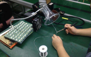
Package on package pop assembly is the SMT assembly process used to build the stacked PoP structure. It includes solder paste printing, bottom package placement, top package dipping, top package placement, reflow soldering, and X-ray inspection.

Q6: Why is X-ray inspection important for PoP?
PoP solder joints are hidden under the packages and between package layers. X-ray inspection helps check solder bridging, open joints, voids, and alignment problems.

Q7: What are package on package pop assembly balls?
They are solder balls used to connect the top package to the bottom package and the bottom package to the PCB. Their size, pitch, and coplanarity directly affect assembly reliability.

Q8: What is TMV in PoP packaging?
TMV means Through-Mold Via. It is a vertical interconnect technology used in advanced PoP packages to support thinner and denser package structures.

Q9: Is PoP suitable for every PCB project?
No. PoP is most useful when PCB space is limited and high integration is required. For simple or low-cost products, standard side-by-side component placement may be enough.

Q10: What files should I provide for a PoP assembly quotation?
You should provide Gerber files, BOM, pick-and-place file, assembly drawing, datasheets for the top and bottom packages, and any special inspection or testing requirements.

To conclude, PoP Package on Package is a stacked IC packaging method that places one package on top of another to save PCB space, improve integration density, and support compact electronic system design. This article explained what PoP means, how package on package PoP works, how PoP assembly is handled, why ball grid and ball layout matter, how SMT supports high-density PoP production, and where TMV PoP is used.

For product teams, the main value of PoP is clear: it helps combine logic and memory in a smaller area while supporting modern compact electronics. But the process also requires accurate PCB design, compatible package selection, controlled SMT assembly, and reliable inspection.

EBest Circuit (Best Technology) supports high-density PCB manufacturing and PCBA assembly for products that use BGA, fine-pitch components, PoP Package on Package, and advanced SMT assembly. Our team can help review your PCB files, BOM, component package details, and inspection requirements before production.

For PoP Package on Package assembly support or PCBA quotation, please contact us at sales@bestpcbs.com.

You may also like

BGA Assembly
Wednesday, March 18th, 2026

BGA Assembly (Ball Grid Array Assembly) is a PCB assembly process where components are mounted using an array of solder balls underneath the package instead of leads. It provides higher connection density, better thermal performance, and improved electrical reliability, making it ideal for high-speed and high-performance electronics such as CPUs, GPUs, and communication devices.

BGA Assembly is a critical process in modern electronics, enabling high-density, high-speed, and high-reliability PCB designs. In this guide, you will understand BGA PCB assembly from process control to supplier selection, helping you reduce defects and improve production stability.

BGA Assembly

BGA Assembly

Looking for Reliable BGA Assembly? Why Right Partner Is Important?

Many projects encounter hidden failures during BGA assembly, especially when scaling from prototype to mass production. Since solder joints are located beneath the package, defects cannot be seen directly and often appear only after testing or field use.

Typical challenges include:

  • Hidden defects such as voids and head-in-pillow
  • Warpage during reflow causing open joints
  • Inconsistent yield across production batches
  • Difficult inspection and rework
  • Reliability risks under thermal cycling

Because of these risks, selecting the right bga pcb assembly manufacturer becomes a key factor in product success rather than a simple sourcing decision.

EBest Circuit – How We Serve You?

EBest Circuit (Best Technology) provides one-stop bga assembly services, including PCB fabrication, component sourcing, SMT assembly, inspection, and final delivery. With over 20 years of experience, we focus on both engineering support and stable production.

What we provide:

  • Turnkey BGA PCB assembly service
  • DFM & DFA support before production
  • Quick turn prototyping and mass production
  • Advanced inspection (SPI + X-ray + AOI)
  • Certified system (ISO9001, ISO13485, IATF16949, AS9100D)

Our goal is not only to assemble boards, but to reduce risk and improve yield from the beginning.

Our BGA Assembly Capabilities

BGA assembly requires precision, process stability, and advanced inspection. Our capability is built around real production control and engineering support.

Technical Capabilities

  • Minimum BGA pitch down to 0.3 mm
  • Placement accuracy up to ±25 µm
  • Support for uBGA, CSP, LGA, PoP, fine-pitch BGA
  • Double-sided SMT and mixed assembly (SMT + THT + BGA)
  • HDI, multilayer, and high-speed PCB support
  • Lead-free and RoHS-compliant processes
  • Full support from prototype to mass production
  • 100% X-ray inspection available for BGA joints
  • SPI inspection for solder paste volume control
  • Multi-zone reflow profiling for thermal consistency
  • BGA rework capability with dedicated stations
  • Void rate control typically <10%
  • Support for tight-pitch, high-density PCB layouts
  • MSL-controlled component handling
  • ESD-controlled production environment
  • Functional testing and validation support
  • Quick turn service for urgent projects

What Is BGA Assembly and Why Is It Critical in Modern PCB Design?

BGA assembly is a process where components with solder balls are mounted onto PCB pads and soldered during reflow. Compared with traditional packages, BGA provides higher pin density and shorter signal paths.

This makes it essential for:

  • High-speed signal transmission
  • Compact electronic devices
  • Better thermal dissipation
  • High-performance computing and communication systems

As product complexity increases, BGA PCB assembly becomes a standard requirement rather than an option.

What Makes BGA PCB Assembly So Challenging?

BGA assembly introduces several technical challenges due to its structure and process sensitivity. Even small deviations can lead to hidden defects.

Key challenges include:

  • Invisible solder joints under the package
  • Thermal warpage during reflow
  • Head-in-pillow defects
  • Solder voids affecting reliability
  • Complex and costly rework process

Because of these factors, advanced process control and inspection are required.

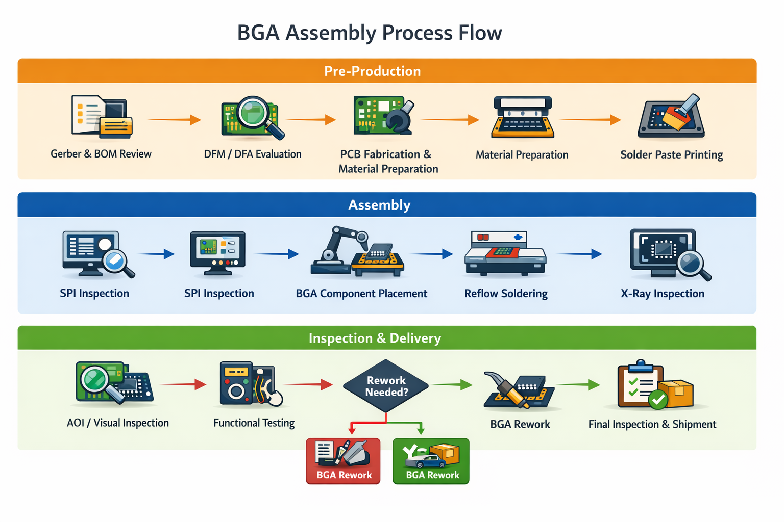
How Does the BGA Assembly Process Work Step by Step?

BGA assembly follows a tightly controlled workflow, because each stage directly affects solder joint reliability and final product performance. A typical BGA PCB assembly process can be summarized as follows:

How Does the BGA Assembly Process Work Step by Step?

To make the process easier to understand, each step serves a specific purpose in controlling quality and reducing hidden BGA defects:

1. Gerber & BOM Review
First, the engineering team reviews the design files and bill of materials to confirm manufacturability and component availability.

2. DFM / DFA Evaluation
Next, design for manufacturability and design for assembly checks are performed, helping identify risks such as pad mismatch, spacing issues, or thermal concerns before production starts.

3. PCB Fabrication & Material Preparation
After that, the PCB and components are prepared, while moisture-sensitive devices are handled according to proper storage and baking requirements.

4. Solder Paste Printing
Then, solder paste is printed onto the PCB pads with carefully controlled volume, because excessive or insufficient paste can directly affect BGA joint quality.

5. SPI Inspection
Before placement, solder paste inspection verifies paste height, area, and consistency, which helps reduce process variation early.

6. BGA Component Placement
The BGA device is then placed using high-precision pick-and-place equipment, ensuring accurate alignment between the solder balls and PCB pads.

7. Reflow Soldering
Next, the board passes through the reflow oven, where the solder balls melt and form electrical and mechanical connections under a controlled temperature profile.

8. X-ray Inspection
Since BGA joints are hidden beneath the package, X-ray inspection is used to check for voids, bridging, opens, and insufficient solder wetting.

9. AOI / Visual Inspection
In addition, visible components and surrounding areas are inspected to confirm overall assembly quality.

10. Functional Testing
Once inspection is complete, electrical and functional tests are performed to verify that the assembled board works as intended.

11. Rework if Needed
If defects are detected, qualified technicians use dedicated BGA rework equipment to remove and replace the component under controlled conditions.

12. Final Inspection & Shipment
Finally, the board goes through final quality verification before packaging and shipment.

Each parameter must be tightly controlled to ensure stable solder joints and minimize defects.

What Equipment Is Required for High-Quality BGA Assembly?

High-quality BGA assembly depends on both equipment and process control.

  • High-precision pick-and-place machines
  • Multi-zone reflow ovens
  • SPI systems for solder paste inspection
  • X-ray inspection systems
  • AOI systems

Among these, X-ray inspection is essential because it allows detection of hidden solder defects.

China BGA PCB Assembly vs Your Local Manufacturing

Choosing between China BGA PCB assembly and local manufacturing depends on project priorities.

FactorChinaLocal
Cost20–40% lowerHigher
CapabilityAdvancedVaries
Lead timeCompetitiveFaster locally
ScalabilityHighMedium

For many companies, China offers a strong balance between cost and capability.

Which Industries Require Advanced BGA Assembly Services?

BGA assembly is widely used in:

  • Consumer electronics
  • Automotive systems
  • Industrial control
  • Medical devices
  • Aerospace

These industries require both performance and reliability.

How to Choose the Right BGA PCB Assembly Manufacturer?

When selecting a partner, focus on both technical capability and process control.

Key factors include:

  • Proven BGA assembly experience
  • X-ray and inspection capability
  • Process control and thermal profiling
  • Quality certifications
  • Engineering support

A reliable partner helps reduce defects and improve production consistency.

FAQs about BGA Assembly Services

1. What are the main advantages of BGA over QFP?

The primary advantage of Ball Grid Array (BGA) over Quad Flat Package (QFP) is its higher connection density. Since BGAs use the entire bottom surface for interconnects rather than just the perimeter, they allow for hundreds of pins in a smaller footprint. Additionally, BGAs offer better thermal dissipation and lower parasitic inductance, which improves high-speed signal integrity.

2. Can BGA components be inspected visually?

No, BGA solder joints cannot be inspected with the naked eye or standard optical equipment because they are hidden beneath the component body. To ensure joint integrity, manufacturers use Automated X-Ray Inspection (AXI) to look through the package and detect defects like solder voids, bridging, or insufficient wetting.

3. What is the most common cause of BGA assembly failure?

The most common cause of BGA failure is an incorrect reflow temperature profile. If the temperature rises too quickly or unevenly, it can lead to “popcorning” (internal package cracking due to moisture), solder ball bridging (shorts), or “head-in-pillow” defects where the solder ball and paste fail to merge.

4. Can you hand-solder a BGA package?

While technically possible for advanced hobbyists with a hot air station, hand-soldering BGAs is not practical or recommended for production. BGAs require precise alignment and a specific thermal profile that can only be consistently achieved using automated pick-and-place machines and multi-zone reflow ovens.

5. Why is “underfill” used in BGA assembly?

Underfill is a specialized epoxy resin injected under the BGA package after soldering. It is used to improve the mechanical reliability of the device by spreading the stress of thermal expansion and physical shock (like dropping a phone) across the entire component rather than just the individual solder balls.

6. What is a “Fine-Pitch” BGA?

A Fine-Pitch BGA (FPBGA), sometimes called a MicroBGA, refers to components where the distance between the centers of the solder balls (the “pitch”) is 0.8mm or less. As the pitch decreases to 0.5mm or 0.4mm, the assembly process becomes significantly more challenging, often requiring advanced PCB technologies like “via-in-pad” to route signals.

Ready for Fast and Reliable BGA Assembly? Get a Quote Today

If you are looking for a reliable bga pcb assembly manufacturer, EBest Circuit is ready to support your project.

  • DFM feedback within 24 hours
  • Process optimization suggestions
  • Fast quotation

Contact: sales@bestpcbs.com

You may also like

BGA Assembly Manufacturer in China, Over 19 Years
Tuesday, October 21st, 2025

Why choose BGA assembly? Let’s discover definition, pros and cons, application, assembly process, quality control methods, package types for BGA assembly.

Are you troubled with these problems?

  • Solder joint voiding/shorting causing yield stuck below 95%?
  • Struggling with 01005 components & 0.25mm BGA pitch—high density, long cycle times?
  • Prototype validation taking 7 days? Slowing time-to-market?

As a BGA assembly manufacturer, EBest Circuit (Best Technology) can provide you service and solutions:

  • Solder joint precision ≤0.02mm, yield >99.8%: eliminate voiding/shorting, cut rework costs by 30%.
  • Full support for 01005/2mil trace/space/0.25mm BGA pitch: over 5,000 solder joints per board, 40% smaller size with 50% higher functionality.
  • 7-day rapid prototyping: 4 SMT lines + 2 BGA lines sync operation, 40% faster than industry average, doubles product lifespan.

Welcome to contact us if you have any inquiry for BGA assembly service: sales@bestpcbs.com.

What Is BGA Assembly?

BGA Assembly is an advanced packaging process that achieves electrical connection between integrated circuits (ICs) and printed circuit boards (PCBs) through an array of solder balls arranged at the bottom. Its core feature lies in replacing traditional pins with tin balls, forming high-density, low-resistance interconnection structures via reflow soldering technology. This approach is particularly suited for high-pin-count, high-performance chips such as processors and GPUs.

What Is BGA Assembly?

What Are Pros and Cons of BGA Assembly Service?

Advantages of BGA Assembly Service

  • High density and miniaturization: Ball grid array layout increases pin count per unit area by 30%-50%. For equivalent capacity, its volume is only one-third of TSOP packages, suitable for miniaturization needs of high-pin-count chips like CPUs and GPUs.
  • Superior electrical performance: Short-path design reduces parasitic inductance/capacitance, cutting signal transmission delay by 40%-60%. Supports high-frequency applications above 100MHz and high-speed communication with 2-3 times improved crosstalk resistance.
  • Outstanding thermal efficiency: Solder balls increase contact area by 3-5 times. Combined with metal substrates or thermal materials, chip operating temperature decreases by 15-20°C, ideal for high-power scenarios like servers and automotive electronics.
  • High mechanical reliability: Solder ball structure buffers thermal expansion stress, improving shock resistance by 50%. Suitable for vibration-prone environments like mobile devices and industrial controls, reducing failure rates by 30%.
  • Optimized production efficiency: Reflow soldering self-alignment reduces placement errors, improving yield by 10%-15%. Automated equipment supports mass production, cutting costs by 20%-30%

Disadvantages of BGA Assembly Service

  • Complex inspection and repair: Requires X-ray/industrial CT for internal defect detection (e.g., voids, cracks) with high equipment costs. Rework needs specialized hot air guns or laser reflow devices. BGA becomes non-reusable post-removal, increasing repair costs by 50%-100%.
  • High costs and technical barriers: Materials (e.g., lead-free solder balls), equipment (high-precision pick-and-place machines), and inspection costs are 30%-50% higher than traditional QFP packaging. Process control requires ±0.05mm placement accuracy.
  • Environmental sensitivity: Requires strict storage conditions (humidity <10% RH, temperature 20-25°C). Prolonged logistics may cause solder ball oxidation, affecting welding quality.
  • Coplanarity and warpage risks: Full-array packaging demands coefficient of thermal expansion (CTE) matching between substrate and PCB (difference <5ppm/°C). Otherwise, coplanarity errors or post-soldering warpage may cause voids or shorts.
  • Competition from alternative technologies: Faces competition from CSP, flip-chip, and other packaging technologies. Requires continuous innovation (e.g., 3D stacked BGA) to maintain market edge, increasing R&D costs by 20%-30%.
What Are Pros and Cons of BGA Assembly Service?

Applications of BGA Assembly

  • Smartphones and tablets: Processors, memory chips, and RF modules.
  • Laptops: CPUs, GPUs, and mainboard components.
  • Server systems: Data center CPUs, GPUs, and storage controllers.
  • High-end graphics cards and workstations: High-speed computing modules.
  • 5G base stations and network equipment: Switch/router integrated circuits.
  • Automotive systems: ADAS domain controllers, navigation units, and control modules.
  • Industrial automation: Microprocessors for harsh environment equipment.
  • Aerospace systems: Satellite/radar microprocessors and image processors.
  • Medical devices: CT machine data processors and patient monitor chips.
  • AI and quantum computing: Multi-chip module (MCM) integration platforms.

What Problems Can BGA Assembly Solve?

  • Enhanced Routing Density: BGA’s bottom grid array design achieves over 1,000 I/O integrations at 0.4mm pitch, increasing pin density by 3-5x compared to traditional QFP packaging. This resolves routing constraints in compact spaces like smartphones and servers. For instance, 0.3mm pitch BGA with laser soldering technology improves ball placement yield to 99.7%, enabling high-density layouts.
  • Signal Stability Optimization: Differential routing and impedance matching (e.g., PCIe 85Ω/100Ω standards) minimize high-speed signal crosstalk and reflections in 5G base stations and high-end GPUs. Blind/buried via technology shortens signal paths, reducing losses and ensuring stability in high-frequency scenarios.
  • Thermal Efficiency Improvement: Spherical solder joints expand heat dissipation area, combined with ceramic substrates, thermal via arrays, and heat sinks, to address overheating in high-power chips like GPUs and FPGAs, extending device lifespan.
  • Process Reliability Enhancement: X-ray inspection and SPC (Statistical Process Control) mitigate hidden defects like voiding and opens in solder joints. Moisture sensitivity classification (per J-STD-020) and baking processes prevent package warpage, while CTE-matched designs reduce solder fatigue in automotive/industrial environments.
  • Cost-Performance Balance: Standardized packaging supports automated SMT assembly, while HDI (High-Density Interconnect) technology optimizes routing density. This balances performance upgrades with PCB layer count and material cost control, ideal for mass production in consumer electronics. For example, PBGA packaging reduces costs by 30% compared to CBGA while maintaining electrical performance.

Common BGA Package Types

PBGA (Plastic Ball Grid Array)

  • Substrate: BT resin/glass laminate, solder balls made of 63Sn37Pb eutectic or lead-free solder.
  • Features: Low cost, good thermal matching (CTE ≈14ppm/°C), compatible with PCB (CTE ≈17ppm/°C), supports self-alignment soldering.
  • Applications: Consumer electronics chips like CPUs and GPUs, e.g., Intel Pentium II/III/IV processors.
  • Limitations: Susceptible to moisture (requires moisture-proof packaging), reliability affected by “popcorn effect,” slightly taller than QFP.

CBGA (Ceramic Ball Grid Array)

  • Substrate: Multilayer ceramic, solder balls use 10Sn90Pb high-temperature solder, requires low-temperature solder for auxiliary connection.
  • Features: Excellent air tightness (moisture resistance), low thermal conductivity (ceramic substrate CTE ≈7ppm/°C), superior heat dissipation, good electrical insulation.
  • Applications: High-reliability scenarios like aerospace and military, early Intel Pentium Pro processors.
  • Limitations: High cost, significant thermal expansion coefficient difference with PCB (causing thermal stress), solder joint fatigue failure risk.

TBGA (Tape Ball Grid Array)

  • Substrate: PI multilayer wiring substrate, solder balls use high-melting-point solder (e.g., 10Sn90Pb), soldered with low-melting-point solder.
  • Features: Ultra-thin profile (thickness ≤1mm), better heat dissipation than PBGA, good thermal matching with flexible tape and PCB.
  • Applications: Mobile devices and high-frequency communication chips, e.g., smartphone processors.
  • Limitations: Moisture sensitivity, reliability affected by multi-material combinations, larger self-alignment deviation.

FCBGA (Flip-Chip Ball Grid Array)

  • Structure: Chip flip-mounted, connected to substrate via gold bumps or high-lead solder (e.g., 90Pb10Sn).
  • Features: High density (pin count >1000), short signal paths (low inductance/capacitance), supports 3D stacking.
  • Applications: High-performance computing like server CPUs/GPUs, Intel Pentium III mobile processors.
  • Limitations: Complex process, requires precise placement accuracy (±0.05mm), underfill needed for mechanical strength.

CCGA (Ceramic Column Grid Array)

  • Structure: Solder columns (diameter 0.5mm, height 1.25-2.2mm) replace solder balls, mitigating thermal stress.
  • Features: Strong fatigue resistance, suitable for high-vibration environments (e.g., automotive electronics).
  • Applications: Industrial controls, automotive ECUs, long-term reliability scenarios.

Micro BGA/High-Density BGA

  • Features: Solder ball pitch ≤0.5mm (Micro BGA) or ≤0.3mm (high-density BGA), pin density increased by 300%.
  • Applications: Portable devices (e.g., smartwatches), high-performance microprocessors, ultra-thin design (thickness <1mm).
  • Challenges: Requires X-ray/CT inspection for internal defects, high repair costs, sensitive to humidity (<10% RH).

EBGA (Enhanced Ball Grid Array with Heatsink)

  • Structure: Integrated metal heatsink or thermal spreader for enhanced heat dissipation.
  • Applications: High-power chips (e.g., server CPUs), optimized thermal performance via thermal interface materials (TIMs).
Common BGA Package Types

BGA Assembly Process Flow

1. Solder Paste Printing Precision Control

  • Utilize 0.12-0.15mm thick stencils with laser-cut apertures to ensure solder paste volume deviation ≤10% for 0.4mm pitch BGA pads. For sub-0.3mm fine-pitch applications, adopt Type 4 solder paste (particle size 15-25μm) with printing speed 30-50mm/s and squeegee pressure 5-10N to prevent solder defects like insufficient solder, bridging, or collapse. Implement AOI systems for real-time monitoring and automatic adjustment for pads with ≥0.1mm misalignment.

2. 3D SPI Detection & Closed-Loop Feedback

  • Employ phase-measuring profilometry (PMP) 3D SPI technology for full-field detection of solder paste volume, height, and shape, unaffected by PCB color/reflection. Data feeds back to the printer for dynamic adjustment of squeegee pressure or stencil cleaning. Integrate SPC control to trigger automatic alarms for consecutive critical defects, enabling proactive process optimization.

3. High-Precision Placement & Vision Alignment

  • Placement machines achieve positioning accuracy ≤±0.03mm and repeatability ≤±0.015mm, with nozzles matched to BGA size/weight. Control placement pressure within 5-20N to avoid PCB warping or pad damage. Post-placement verification via dual-camera vision systems ensures alignment accuracy <1/4 pad diameter; misalignment >0.1mm triggers automatic rework.

4. Reflow Soldering Profile Optimization

  • Customize four-stage temperature profiles based on solder paste melting points (e.g., 217-227°C for lead-free solder): preheat (150-180°C/60-90s), soak (180-210°C/30-60s), reflow (peak 20-30°C above melting point/30-45s), and cooling (≤4°C/s gradient). Nitrogen atmosphere (O₂ <500ppm) reduces oxidation and void rates. Control furnace temperature uniformity within ±2°C and conveyor speed 50-100cm/min.

5. Multi-Stage Cleaning & Residue Control

  • Remove flux residues using water-based/semi-aqueous cleaning processes to prevent ionic contamination. For BGA pads, employ specialized cleaners with solder wick to ensure surface flatness. Post-cleaning X-ray inspection verifies solder joint quality, with void rates <25% and no defects like cold joints or bridges.

6. X-ray & AOI Synergistic Inspection

  • 3D X-ray CT scans detect internal defects (voids, cracks, missing solder balls), while 2D X-ray focuses on center and perimeter regions. Post-reflow AOI performs three-point correlation analysis to trace defect origins. Data links to equipment via IPC-CFX protocol for smart factory integration.

7. Electrical Testing & Functional Verification

  • ICT tests detect solder bridges, opens, and component failures; FT validates circuit continuity and signal integrity. Environmental stress screening (85°C/85%RH/1000h) and ESS accelerate defect detection. Test coverage meets AQL 1.0 standards for reliability assurance.

8. Rework Process & Quality Control

  • Use hot-air rework stations for BGA removal (preheat ≤120°C, removal temperature matching peak reflow profile). Clean pads and re-place components with secondary vision alignment. Post-rework executes 100% X-ray inspection and functional testing per IPC-7095C standards, with full process data logged for traceability.
BGA Assembly Process Flow

Quality Inspection Methods for BGA Assembly

1. Visual Inspection and Surface Defect Screening

  • Application Scenario: First-article and in-process monitoring on production lines.
  • Technical Points: Use high-magnification microscopes (≥20X) to inspect solder ball appearance, focusing on bridges, solder balls residue, solder collapse, and oxidation. According to IPC-A-610 standards, the solder wetting angle must be ≤90°, with pad coverage ≥75%.
  • Limitations: Only detects surface defects; cannot evaluate internal joint integrity.

2. X-ray Inspection Technology (2D/3D)

  • 2D X-ray: Uses planar imaging to detect two-dimensional defects like solder shift, shorts, or insufficient solder volume. Overlapping depth data may cause misjudgment (e.g., stacked layer shadows). Equipment like the YXLON Cougar S series achieves 1μm resolution.
  • 3D X-ray (CT Scanning): Employs tomography for 3D modeling, quantifying void ratios, crack lengths, and interface bonding states. Per IPC 7095, Class 3 products require void diameters ≤30% (or area ≤9%); medical/military sectors demand ≤25%. Space-grade BGA mandates total void area ≤5%.

3. Ultrasonic Scanning Acoustic Microscopy (C-SAM)

  • Principle: Utilizes 50MHz ultrasonic waves to detect delamination, voids, and interface defects via reflection differences. Excels at identifying microvoids ≤50μm.
  • Case Study: Automotive MCUs undergo C-SAM validation post -40°C~125°C thermal cycling, requiring delamination area ≤10% of joint cross-section. “Popcorn effect” (moisture-induced cracking) is detectable via abnormal attenuation coefficients.

4. Thermal Imaging Testing

  • Thermal Analysis: Infrared thermal cameras monitor temperature distribution during BGA operation; faulty joints show ≥5°C abnormal rises. Dynamic load testing locates thermal failure points.

5. Electrical Performance Testing

  • Electrical Test Systems: ICT/Flying Probe: Tests open/short circuits via PCB contact points; 0.4mm-pitch BGA requires spring-loaded probe arrays (±0.02mm accuracy).
  • Boundary Scan (JTAG): IEEE 1149.1-compliant chip self-testing verifies logic functions and pin connectivity with ≤0.1% false error rates.
  • High-Frequency Signal Testing: 1GHz+ signals demand insertion loss ≤0.5dB, phase shift ≤5°, using shielded chambers (≥80dB@1GHz) to avoid EMI.

6. Destructive Physical Analysis

  • Red Dye Penetration Test: Dye penetration visualizes voids/cracks in joint cross-sections. Requires 100°C/4h baking for dye curing, with ≥25mm cutting margins to prevent artificial damage.
  • Shear Strength Testing: JEDEC standards mandate 6gf minimum shear force for 0.8mm-pitch balls; automotive-grade components require ≤15% strength degradation post-125°C/2000h aging.
  • Metallographic Cross-Section Analysis: Samples embedded in cold resin undergo grinding/polishing for SEM crack analysis (≤50μm acceptable), paired with EDS for elemental anomaly detection.

7. Environmental Stress and Reliability Verification

  • Thermal Cycling: -40°C~125°C for 1000 cycles (500 cycles for industrial), 1h per cycle; crack growth ≤50μm. Automotive-grade components require AEC-Q200 certification for 10-year equivalent lifespans.
  • Humidity Testing: 85°C/85%RH for 1000h; insulation resistance ≥10MΩ, solder corrosion ≤5%.
  • Mechanical Shock: 1500g/0.5ms pulse simulates drop impacts; no package detachment or joint cracking.

    Why Choose EBest Circuit (Best Technology) as BGA Assembly Manufacturer?

    Reasons why choose us as BGA assembly manufacturer in China:

    • Ultra-Precision BGA Ball Placement Process with Yield Exceeding 99.8%: Achieves solder ball position accuracy ≤0.02mm through precision mechanical calibration and multi-stage verification, eliminating void soldering/short-circuit risks while reducing client rework costs by over 30%.
    • Ultra-Fine Pitch PCBA Integration Capability: Supports 01005 component packaging, 2mil line width/spacing, and 40μm laser microvias. Enables integration of over 5,000 BGA solder joints per board, reducing product volume by 40% while increasing functional density by 50%.
    • 7-Day Rapid NPI Verification Service: Four fully automated SMT lines + two dedicated BGA packaging lines enable prototype delivery within 7 days, 40% faster than industry average, accelerating time-to-market for clients.
    • DFM-Driven Cost Optimization Solution: Optimizes BGA packaging layers through Design for Manufacturability (DFM) analysis, combined with cost-effective material substitution and bulk procurement advantages, reducing total PCBA costs by 15% for enhanced market competitiveness.
    • End-to-End Transparent Quality Control: MES system enables full barcode traceability from material intake to final shipment, with real-time cloud synchronization of critical process parameters. Clients gain instant access to production progress and quality reports for zero-distance quality monitoring.
    • Green Manufacturing Compliance System: Uses lead-free solder paste and halogen-free substrates with 100% compliant wastewater/gas emissions. ISO 14001 certified, ensuring seamless compliance with EU RoHS/REACH regulations to avoid trade barriers.
    • Multi-Scenario Failure Analysis Support: Equipped with X-ray inspection, ultrasonic scanning microscopy, and cross-section analysis tools. Offers 24/7 failure analysis services with root cause reports delivered within 48 hours to minimize production line downtime.
    • Agile Supply Chain Assurance System: Strategic inventory partnerships with top-tier component manufacturers reduce critical material lead time to 3 days. Multi-site factory coordination ensures stable delivery of large-volume orders while mitigating supply chain risks.

    Our BGA Assembly Capabilities

    ItemCapabilities
    Placer Speed13,200,000 chips/day
    Bare Board Size0.2″ × 0.2″ – 20″ × 20″ / 22″ × 47.5″
    Minimum SMD Component01005 (0.4mm × 0.2mm)
    Minimum BGA Pitch0.25mm (10mil)
    Maximum Components50mm × 150mm (Board Area)
    Assembly TypeSMT / THT / Mixed Assembly
    Component PackageReels / Cut Tape / Tube / Tray / Loose Parts
    Lead Time1 – 5 days (Standard)

    How to Get a Quote for BGA Assembly Services?

    All documents required to obtain a quote for BAG assembly services:

    • Submit Design Files: Provide Gerber files, a bill of materials (BOM) (including BGA model/parameters), PCB design drawings, and 3D models (if available). Ensure the file version is the final production version.
    • Specify BGA technical details: Indicate the BGA pad size, ball diameter, ball pitch (e.g., 0.25mm), package type (e.g., PGA/LGA), and solder requirements (e.g., lead-free/lead-containing).
    • Confirm production capacity and delivery time: Indicate annual demand, batch order quantity, and target lead time (e.g., 7 days/15 days/30 days). Indicate whether expedited service is required.
    • Specify testing standards: Indicate whether X-ray inspection, AOI optical inspection, flying probe testing, or functional testing is required, and whether third-party certification (e.g., AEC-Q100) is required.
    • Indicate material sources: Specify the sourcing method (customer-furnished/contract manufacturing) for BGA chips and other key components, as well as brand preference (e.g., Intel/AMD/Murata).
    • Fill out the Quote Request Form: Submit the Quote Request Form containing the above information via our official website or designated email address, along with contact information and decision-maker information for follow-up.

    Welcome to contact us if you have any request for BGA assembly services: sales@bestpcbs.com.

    You may also like