A PCB jumper creates an intentional connection between two circuit-board nodes for routing, configuration, an approved engineering change, or trace repair. Select it as an electrical and mechanical interconnect: define conductor size, insulation, terminations, routing, clearance, documentation, inspection, and test limits before production.

What Is a PCB Jumper and How Does It Work?
A PCB jumper is a controlled conductive path that joins two nodes to cross, select, bypass, or restore a circuit connection.
- Electrical role: It becomes part of the net’s resistance, inductance, current path, voltage spacing, and test coverage.
- Physical forms: Common implementations include a formed bare link, insulated wire, solder-bridge pads, removable shunt, and zero-ohm component.
- Required definition: Specify both endpoints, default open/closed state, material, installed route, termination method, and acceptance test.
- Bypass check: Confirm that the connection does not defeat a fuse, filter, current limiter, isolation feature, test function, or fault-detection element.
Why Are Jumpers Used in PCB Design, Assembly and Repair?
Use a jumper only for a defined routing, configuration, ECO, assembly-variant, repair, or diagnostic task.
- Routing crossover: A wire link can cross an existing conductor on a single-sided or routing-constrained board without creating an unintended connection.
- Product configuration: A solder jumper or removable shunt can select an address, boot mode, voltage option, feature, or test state.
- Engineering change: A controlled wire connection can implement an approved ECO before a redesigned PCB revision is available.
- Assembly adaptation: A production jumper can support one PCB across several approved variants when the BOM and assembly instructions define each state.
- Trace repair: A jumper wire can restore continuity around an open, lifted, burned, or intentionally cut copper trace after the root cause is understood.
- Debug access: A temporary, controlled connection can support laboratory diagnosis, but it should not silently become a production solution.
What Types of PCB Jumpers Are Available for Different Applications?
Choose the jumper type from the required length, change frequency, assembly method, insulation, current path, and service access.
| Jumper Type | Physical Form | Primary Use | Main Design Control | Key Limitation |
| Bare wire link | Formed solid conductor | Short crossover on controlled boards | Spacing and formed height | Requires controlled clearance from conductive features |
| Insulated wire jumper | Solid or stranded insulated wire | ECO, repair, or longer routing that needs insulation | Gauge, insulation, attachment, routing | Manual routing and attachment can vary |
| Solder jumper | Two or more exposed copper pads | Low-cycle configuration or fixed assembly option | Pad gap, mask opening, solder volume | Repeated rework can damage pads or mask |
| Removable shunt | Conductive cap over header pins | Field or service configuration | Pin pitch, retention, access, labeling | Extra height and removable part |
| Zero-ohm component link | Through-hole or SMT component | Automated assembly and routing option | Package rating and placement process | Not a true zero-impedance path |
- Choose wire: Use it for longer paths, conductor crossovers, repairs, or routes that require insulation.
- Choose solder pads: Use them for compact, low-cycle configuration when soldering and inspection access are available.
- Choose a shunt: Use it when authorized users must change the state without soldering.
- Choose a zero-ohm link: Use it when standard component placement offers better production control than manual wire installation.
How Do Jumper Connection Methods Differ for Production and Configuration?
Select the connection method by who must change it, how often it changes, and how production will install and verify it.
| Decision Dimension | Wire Link | Solder Jumper | Removable Shunt | Zero-Ohm Link |
| Preferred task | Routing, ECO, repair | Assembly configuration | Field configuration | Automated production option |
| Assembly method | Manual or formed-wire insertion | Controlled solder deposit | Header placement plus shunt | Standard component placement |
| Change frequency | Low | Low | Moderate to frequent, within the connector rating | Low |
| Mechanical control | Routing, staking, and strain relief as required | Pad integrity and a low-profile solder bridge | Header retention, access, and enclosure clearance | Land pattern and solder-joint integrity |
| Inspection focus | Joints, insulation, strain relief | Bridge continuity and shorts | Correct pin position, presence, and retention | Placement and solder joints |
| Main risk | Movement or routing damage | Unintended bridge or incomplete wetting | Missing or displaced shunt | Wrong population state |
- High current: Verify conductor and termination temperature; do not select a small solder bridge by convenience.
- Field changes: Prefer a rated removable interface when users must change the state repeatedly.
- Volume production: Prefer the option with the most repeatable placement, inspection, and variant control.
When Should a PCB Jumper Be Used or Avoided in PCB Design?
Use a PCB jumper when it provides a documented, testable connection with lower total risk than a PCB revision or alternative interconnect.
- Suitable uses: A controlled product option, single-sided crossover, approved low-volume ECO, or repair that preserves the intended circuit function.
- Temporary production use: A prototype-to-production change with revision control, a defined removal plan, and complete build/test instructions.
- Safety path: The jumper would bypass a fuse, isolation barrier, current limiter, protective impedance, or required safety spacing.
- Signal sensitivity: The added loop area, stub, or uncontrolled impedance would compromise a high-speed, low-noise, clock, RF, or precision analog net.
- Mechanical exposure: The wire can be pinched, abraded, flexed, contacted by hardware, or moved during service.
- Thermal stress: Expected current or ambient temperature could cause unacceptable conductor or joint heating.
- Process dependence: Correct function relies on an undocumented operator decision rather than a controlled BOM and work instruction.
- Redesign trigger: Revise the PCB when jumper count, routing complexity, inspection difficulty, or manual touch time makes direct copper routing more reliable.
- Regulated products: Accept a jumper only when product risk controls, traceability, environmental qualification, inspection, and customer or regulatory requirements permit it.
How Should Jumper Wire Size Be Selected for Current and Temperature Requirements?
Select jumper wire size from voltage drop, temperature rise, insulation rating, installed length, duty cycle, and termination capability—not from current alone.
- Define current: Record continuous, peak, inrush, fault, and duty-cycle values instead of using only nominal current.
- Set voltage-drop limit: Allocate an acceptable drop for the complete jumper path, including contact and solder-joint resistance.
- Calculate conductor loss: Use R = ρL/A, V = IR, and P = I²R with conductor resistivity at the expected temperature and the actual installed length.
- Check temperature: Evaluate the wire, insulation, solder joints, pads, bundling, enclosure ambient, airflow, and nearby heat sources.
- Check terminations: Confirm that the pad and plated-hole geometry can accept the conductor without poor wetting, pad lifting, or excessive heat input.
- Validate a sample: Measure voltage drop and stabilized temperature at the defined load; record the conditions and acceptance limits.
Example: A 20 mΩ jumper carrying 2 A drops 40 mV and dissipates 80 mW. This calculation does not approve the design; confirm stabilized wire and joint temperatures on the installed assembly because termination resistance can dominate local heating.
How Should Solder Jumper Pads, Spacing and Routing Be Designed?
Design solder jumper pads so the required state is easy to assemble and test without accidental bridging, pad damage, or clearance loss.
- Define the states: Specify whether the default assembly state is open or closed and identify every approved variant.
- Select pad geometry: Provide enough exposed copper for controlled solder wetting without creating an unnecessarily large molten solder mass.
- Set the gap: Choose a gap compatible with the soldering process and with the required open-state resistance and electrical clearance.
- Control solder mask: Define the opening and mask dam so solder bridges only the intended pads; confirm achievable registration and dam limits during DFM.
- Protect neighboring nets: Keep pads, vias, metal hardware, and component terminals far enough away for the voltage, environment, and workmanship process.
- Provide access: Leave room for the soldering tip, inspection optics, cleaning, and electrical probes.
- Label the function: Use an unambiguous reference designator and state marking that matches the schematic, BOM, assembly drawing, and test instruction.
- Route wire safely: Keep a wire jumper short but not taut; avoid sharp bends, hot parts, cutting edges, screw heads, latches, component leads, and moving mechanisms.
- Protect crossings: Use suitable insulation and maintain required spacing along the full installed route when crossing exposed conductors.
- Verify the footprint: Review paste, mask, copper, courtyard, assembly notes, and net assignments before release.
How Do Wire Links Affect Signal Integrity, RF Performance and High-Voltage Safety?
A wire link changes resistance, inductance, loop area, coupling, return-current flow, and spacing; evaluate the installed geometry, not only the schematic connection.
- High-speed digital: Minimize length and stubs, keep the return path close, and avoid reference-plane gaps that force return current around the jumper.
- RF and low-level analog: Control loop area and coupling to reduce ringing, emissions, susceptibility, timing error, and noise pickup; measure the final waveform or RF response.
- Differential and clock nets: Do not introduce uncontrolled skew or impedance discontinuity without analysis and validation.
- High voltage: Determine clearance and creepage from working voltage, transient overvoltage, pollution, altitude, material group, coating, and the applicable product standard. Include wire sag and assembly tolerance.
- Isolation barriers: Do not cross a barrier unless the connection is an intentional, reviewed part of the isolation design.
- Power switching: Check voltage drop, joint temperature, magnetic loop area, nearby sensitive nets, waveforms, and emissions under worst-case load.
How Should a PCB Jumper Be Defined in Schematic, PCB Layout, BOM and Assembly Files?
Define every PCB jumper in the files that control connectivity, material, installation, variant state, and acceptance.
- Schematic: Give the jumper a reference designator, net connection, default state, and functional note. Show whether it is a component, solder bridge, wire link, or approved rework.
- PCB layout: Include the correct footprint, pad or hole geometry, routing keepouts, assembly clearance, and installed-wire path when the path is controlled.
- BOM: Define the wire or component specification, insulation, conductor construction, length or preparation rule, population state, and approved alternates where applicable.
- Assembly drawing: Show termination points, route, maximum loop height, bend direction, attachment locations, polarity or orientation if relevant, and open/closed variant states.
- ECO record: State the reason, affected revisions, exact cut/add operations, inspection, test, disposition, and planned incorporation into the next design revision.
- Test instruction: Identify the expected continuity, resistance, voltage, function, and configuration result for each approved state.
Release check: Compare the actual net, state, endpoints, material, and route across files. File presence alone does not detect a schematic marked “closed” while the BOM omits the link or the drawing points to the wrong pad.
How Are Production Jumpers Manufactured, Installed and Inspected During PCB Assembly?
Install production jumpers through a revision-controlled process with defined material, routing, soldering, inspection, and electrical acceptance.
- Confirm the revision: Verify the approved BOM, assembly drawing, ECO, route, and connection state before material is issued.
- Verify material: Check conductor type, gauge, insulation, color if controlled, length, stripping requirement, and lot traceability required by the project.
- Prepare the wire: Cut, strip, form, and tin only as the approved work instruction permits. Avoid nicking strands or reducing conductor area.
- Prepare the board: Confirm pad condition, cleanliness, accessibility, and absence of damage around both termination points.
- Install the connection: Place the conductor without tension, excessive slack, sharp bends, or contact with prohibited components and edges.
- Solder the terminations: Apply a qualified soldering profile or manual process that achieves wetting without burning insulation, overheating pads, or leaving exposed strands.
- Clean and inspect: Remove residues when required and inspect solder shape, wetting, conductor entry, insulation setback, route, clearance, and foreign material.
- Secure the wire: Add approved attachment or strain relief where movement, vibration, length, or service handling creates mechanical risk.
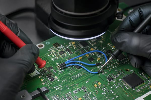
- Perform electrical tests: Confirm the required continuity, isolation, resistance, voltage drop, and functional state.
- Record acceptance: Retain the inspection and test evidence required by the drawing, quality plan, ECO, or customer specification.
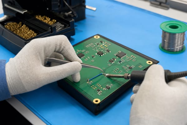
Use both workmanship and electrical evidence: visual inspection cannot prove the net is correct, while continuity cannot prove acceptable routing or strain relief. IPC-A-610J includes jumper-wire acceptance requirements; the drawing and contract must still identify the applicable class and project-specific criteria.
How Can a Broken PCB Trace Be Repaired with a Jumper Wire?
Repair a broken trace with jumper wire only after identifying the failure cause, confirming the net, and proving that repair is permitted for the product.
- Find the root cause: Determine whether the trace opened because of mechanical damage, overcurrent, corrosion, overheating, a manufacturing defect, or an intentional cut.
- Confirm the net: Use the schematic, layout data, and measurement to identify both connection points and verify that no protection element is being bypassed.
- Remove unstable damage: Clean carbonized, lifted, contaminated, or loose material as allowed by the approved repair procedure.
- Select termination points: Use sound pads, vias, component leads, or exposed conductor locations with adequate mechanical strength and electrical access.
- Select the jumper: Match conductor size, insulation, length, and temperature capability to the current, voltage, environment, and repair geometry.
- Route and solder: Keep the path controlled, avoid tension and hazards, and form acceptable solder joints without damaging adjacent features.
- Secure the repair: Apply approved strain relief when wire length or product loading could transfer force to the terminations.
- Inspect and test: Verify workmanship, continuity, isolation, resistance or voltage drop, and complete circuit function under appropriate load.
- Document the repair: Record the board identity, revision, defect, repair method, operator or process record, inspection, test result, and disposition.
- Approved method: The repair procedure may use IPC-7711/21D for rework and printed-board circuit repair, but product authorization and acceptance criteria must be defined.
- Burn damage: Correct the overcurrent, contamination, spacing, or thermal cause before restoring copper; otherwise the repaired path can fail again.
- Scrap decision: Require engineering disposition for high-energy, high-voltage, high-frequency, safety-related, carbonized, or structurally damaged areas.
Which Jumper Defects and Reliability Problems Should Be Avoided?
Control each jumper defect with a defined cause, detection method, and preventive action.
| Defect or Risk | Likely Cause | Detection Method | Preventive Control |
| Wrong connection | Drawing, netlist, or ECO mismatch | Netlist-based continuity/isolation and functional test | File-to-file release review |
| Intermittent joint | Poor wetting, contamination, or strain | Visual inspection plus continuity or resistance while applying the approved movement or stress | Qualified soldering and strain relief |
| Pad lifting | Excess heat or mechanical force | Magnified inspection | Controlled heat input, dwell time, and wire strain |
| Insulation damage | Hot tools, sharp edges, or abrasion | Route inspection plus insulation-resistance or withstand testing when specified | Protected routing and attachment |
| Excessive heating | Undersized conductor or high-resistance joint | Voltage-drop and temperature test | Current analysis and loaded validation |
| Unintended short | Loose strands, solder splash, or low clearance | Visual inspection and adjacent-net isolation test | Controlled stripping, soldering, and spacing |
| Wire fatigue | Vibration, repeated flexing, or unsupported length | Route inspection and product-specific vibration or movement test | Controlled slack, routing, and strain relief |
| Leakage or corrosion | Moisture, ionic residue, or damaged insulation | Cleanliness, insulation-resistance, and environmental testing as specified | Cleaning, spacing, coating when approved, and insulation protection |
What Should Be Verified Before Releasing a PCB with Jumpers for Production?
Release the design only when production can build and verify every jumper from controlled files without verbal instructions.
- Revision control: Identify the approved PCB revision, assembly revision, BOM variant, and ECO status.
- Connectivity: Compare schematic nets, layout pads, jumper states, and test expectations.
- Material definition: Specify wire construction, gauge, insulation, component or shunt part, approved alternates, and preparation.
- Electrical limits: Review current, voltage drop, temperature, signal integrity, isolation, and fault behavior.
- Physical routing: Check length, loop height, bend radius, access, spacing, hardware conflicts, moving parts, and heat sources.
- Workmanship: Define soldering, cleaning, insulation setback, attachment, and acceptable visual condition.
- Test coverage: Assign continuity, isolation, resistance, voltage-drop, thermal, functional, or system tests according to risk.
- Variant control: Make every open/closed or populated/unpopulated state unambiguous in the BOM, drawing, traveler, and software configuration where applicable.
- DFM closure: Resolve pad, mask, hole, access, clearance, and assembly concerns with the manufacturer before release.
- RFQ package: State whether the jumper is an original feature, temporary ECO, or approved repair; provide Gerber or ODB++, schematic where permitted, BOM, assembly drawings, route/state instructions, quantity, attachment requirements, test records, and acceptance criteria.
FAQs About PCB Jumpers
Q1: Can a PCB jumper be installed on either side of the board?
A1: Yes, if the controlled drawing permits it. Verify clearance, soldering access, inspection visibility, enclosure interference, and moving parts on the selected side.
Q2: Does jumper wire color define its electrical function?
A2: No universal PCB jumper color code applies. Color may support assembly control, but the drawing, reference designator, net, and work instruction define function.
Q3: Can a jumper wire run underneath a component?
A3: Only when clearance, heat, compression, inspection, and service access are controlled. Prefer a visible route when hidden placement is not required.
Q4: Can conformal coating be applied over a jumper wire?
A4: Yes, after the jumper passes inspection and test. Confirm coating compatibility with the insulation and joints, and preserve access if later configuration is required.
Q5: Should a PCB jumper use solid or stranded wire?
A5: Use solid wire for stable formed routes and stranded wire where qualified movement tolerance is needed. Stranded wire requires controlled stripping, strand capture, and termination.
Q6: Can a PCB jumper wire include a splice?
A6: Use a splice only when an approved procedure permits it. A continuous conductor normally eliminates an added resistance, insulation, and mechanical failure point.
Q7: Can a solder jumper be opened and closed many times?
A7: No; treat it as a low-cycle configuration feature. Use a rated connector or switch when frequent changes are required.
Q8: Does a PCB jumper need polarity or orientation marking?
A8: A simple wire is not polarized, but its endpoints and installed state must be unambiguous. Mark keyed shunts, crossed routes, and nearby selectable positions.
Q9: Should unused jumper pads remain open?
A9: Keep them in the documented default state. For an open state, inspect and test for solder, contamination, or damage that could create conduction.
Q10: How should assembled boards with exposed jumpers be packaged?
A10: Protect the highest wire loop and both terminations. Use packaging that prevents compression, snagging, abrasion, ESD exposure, and movement during handling and transport.
For PCB jumper design review, fabrication, assembly, ECO implementation, or prototype-to-production support, contact EBest Circuit. Send your Gerber or ODB++, BOM, quantity, stack-up, assembly drawings, jumper instructions, programming method, and test requirements to sales@bestpcbs.com for engineering review and a quotation.