PCB manufacturing PCB manufacturing
Home > Blog

stripline vs microstrip loss

Stripline vs Microstrip: Impedance, Loss, Delay, and PCB Routing
Wednesday, July 29th, 2026

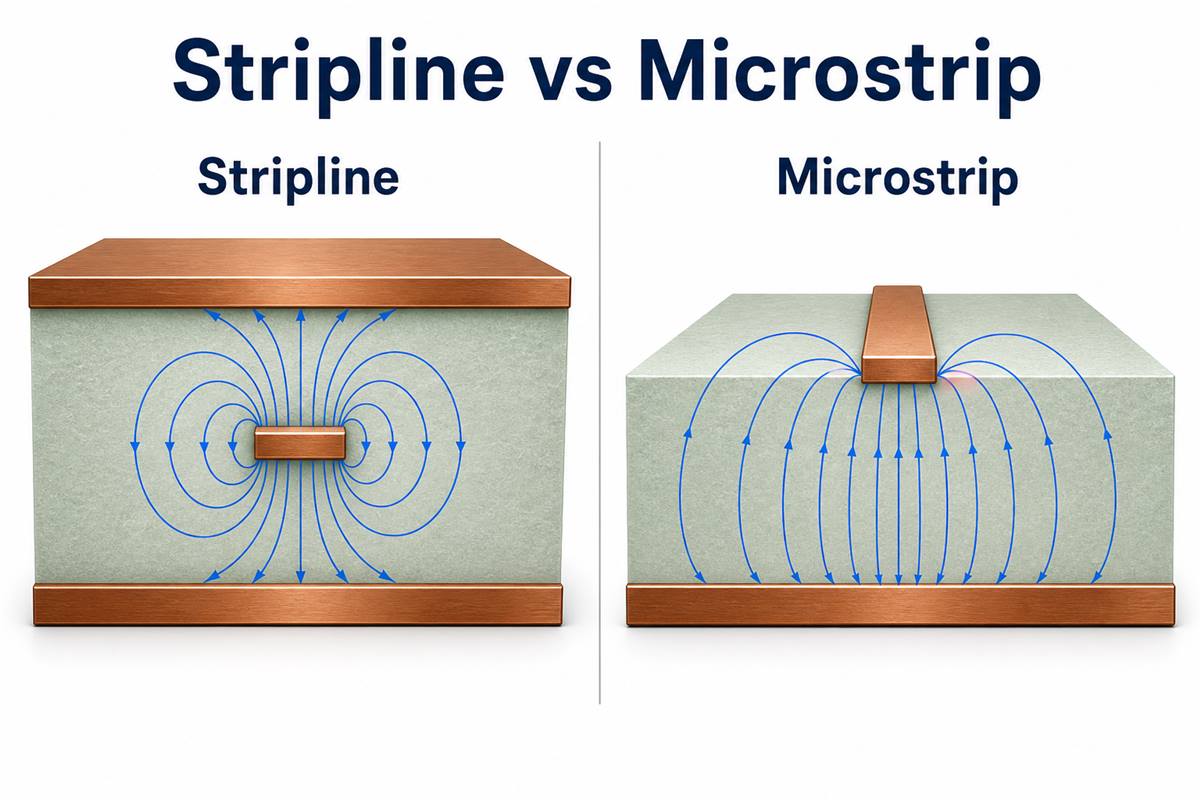
Stripline vs microstrip is a choice between an inner-layer transmission line surrounded by dielectric and an outer-layer transmission line exposed to air and solder mask. Stripline provides stronger field containment and isolation. Microstrip usually gives easier probing, direct access to surface components, and fewer layer-transition vias.

Neither structure is automatically better. The right choice depends on the target impedance, frequency or edge rate, channel length, loss budget, EMI risk, layer count, via transitions, routing density, and manufacturing tolerance. This guide compares those tradeoffs and shows what engineers should define before releasing controlled-impedance PCB data.
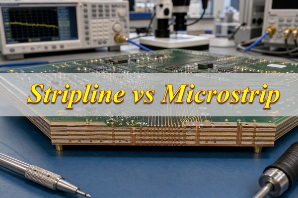
Stripline vs Microstrip PCB cross-section showing field containment

What Is the Difference Between Stripline and Microstrip?

Microstrip is a surface trace referenced mainly to one adjacent plane, while stripline is an internal trace embedded between two reference planes. This placement changes the electromagnetic field, effective dielectric constant, propagation delay, coupling, probing access, and the number of vias needed to reach components.

  • Microstrip: The trace sits on an outer copper layer. Part of its field travels through PCB dielectric and part through air or solder mask, so it behaves as a quasi-TEM transmission line.
  • Stripline: The trace is surrounded by dielectric between two planes. Its field is more tightly contained, and a symmetric structure can approximate a TEM transmission line.
  • Embedded microstrip: A covered outer-layer-like trace under a dielectric layer is not the same as a true stripline. Its field and impedance must be modeled with the actual stackup.
  • Asymmetric stripline: The trace is not centered between its reference planes. Different dielectric heights above and below the trace change its impedance and coupling.

A PCB can use both structures. For example, a short route from a surface BGA pad may begin as microstrip and then change to stripline for a longer, better-contained channel. The transition itself must be included in the channel design.

Stripline vs Microstrip Pros and Cons

The practical differences are field containment, accessibility, propagation environment, layer usage, and transition cost. The table compares the two structures without assuming the same trace width or dielectric spacing.

Design Factor Microstrip Stripline
Trace location Outer PCB layer Inner PCB layer between two planes
Field containment Partly exposed above the board Mostly contained inside dielectric
Component access Direct route to surface pads Normally requires a via transition
Probing and rework Easier to access Hidden after lamination
Layer resources Uses an outer signal layer and one nearby plane Uses an inner signal layer bounded by two planes
Environmental sensitivity Affected by solder mask and material above the trace More stable when the internal dielectric structure is controlled
Isolation More exposed to neighboring fields Usually better field containment and isolation

These are tendencies, not universal performance guarantees. A carefully designed microstrip can outperform a poorly designed stripline channel. Trace length, spacing, material loss, copper roughness, plane continuity, and via geometry still control the result.

The final stripline vs microstrip decision should therefore be based on the complete channel and the producible stackup, not on one isolated advantage.

How Does Stripline vs Microstrip Impedance Differ?

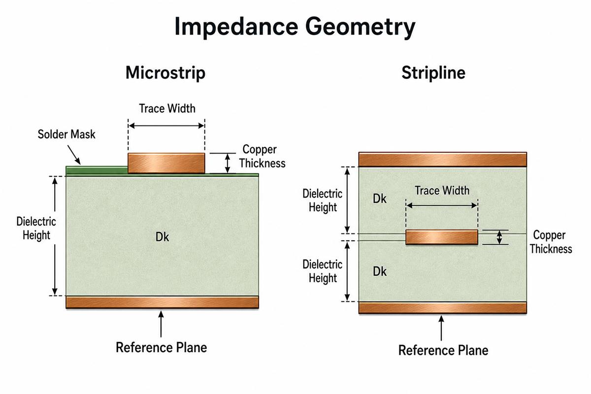
Stripline vs microstrip impedance differs because the electromagnetic field sees different dielectric environments and reference-plane geometry. Neither structure has a fixed characteristic impedance; both must be calculated from the finished production stackup.

Important single-ended impedance inputs include:

  • finished trace width and copper thickness;
  • dielectric height to the reference plane or planes;
  • material Dk at the relevant frequency;
  • etch shape and conductor sidewall profile;
  • solder mask thickness and Dk for microstrip;
  • surface copper plating and final finish;
  • whether the stripline is symmetric or asymmetric.
Impedance geometry inputs for microstrip and stripline PCB traces

For the same target impedance, the required line width can differ substantially between structures. Copying a microstrip width onto an inner stripline layer will not preserve impedance. Start with the fabricator’s proposed stackup, calculate each geometry separately, and then confirm the producible width and spacing.

Which Structure Has Lower Transmission Loss?

There is no universal winner for stripline vs microstrip loss. Stripline keeps its field inside the dielectric and may experience more dielectric loss, while microstrip can suffer more radiation, surface-condition sensitivity, and conductor-related effects. The total channel loss depends on the actual geometry and materials.

Evaluate the following loss mechanisms together:

  • Dielectric loss: Driven by material Df, frequency, field distribution, and route length.
  • Conductor loss: Influenced by finished copper cross-section, skin effect, and copper roughness.
  • Radiation loss: More relevant when fields are less contained or reference paths are disrupted.
  • Discontinuity loss: Added by vias, pads, connectors, neck-downs, stubs, and plane transitions.

Do not compare loss using the same line width alone. A fair comparison holds the target impedance and material system constant, then optimizes the geometry of each structure. Long multi-gigabit or RF channels may require field-solver modeling and insertion-loss simulation rather than a simple closed-form calculator.

How Does Propagation Delay Differ?

Stripline is generally slower than microstrip of the same physical length because its field propagates through the PCB dielectric, while part of a microstrip field travels through air or solder mask with a lower effective permittivity. The exact propagation delay microstrip vs stripline relationship depends on stackup geometry and material Dk.

This difference matters when timing is compared across routes. Two traces with equal physical length can have different electrical delay if one is microstrip and the other is stripline. For clocks, source-synchronous buses, matched RF paths, and multi-lane SerDes:

  • keep matched members on the same transmission-line structure where possible;
  • match electrical delay, not only CAD length;
  • include package, connector, via, and layer-transition delay;
  • use the laminate’s frequency-dependent Dk rather than a generic FR-4 value when timing margin is tight.

The same principle applies when interpreting an eye diagram: additional skew, attenuation, and reflections can reduce eye width and eye height even when the nominal route lengths appear matched.

How Do Differential Pairs Behave in Each Structure?

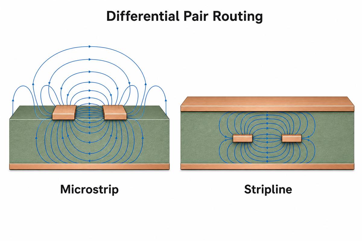
Differential pair stripline vs microstrip requires comparing both the trace-to-plane coupling and the coupling between the two traces. Pair spacing, line width, dielectric height, copper thickness, and reference geometry determine the differential impedance and odd-mode behavior.

Microstrip pairs are accessible and can route directly from surface pads, but their fields are less confined and solder mask affects impedance. Stripline pairs are better contained, but their required widths and spacing must fit the inner-layer design rules. Broadside-coupled stripline is another option, yet layer registration becomes a critical manufacturing variable.
Differential pair routing comparison for microstrip and stripline

Good differential routing practice includes:

  • using one approved geometry for the critical part of the pair;
  • keeping both traces on the same layer and reference structure;
  • avoiding unnecessary uncoupling around pads and vias;
  • minimizing pair skew without adding excessive serpentine coupling;
  • defining both the differential target and any single-ended constraint required by the interface.

Which Structure Controls EMI and Crosstalk Better?

Stripline generally provides better field containment because the signal trace is bounded by two reference planes. That can reduce emissions and coupling to other circuits, but it does not correct poor spacing, plane voids, long parallel routes, or a badly designed via transition.
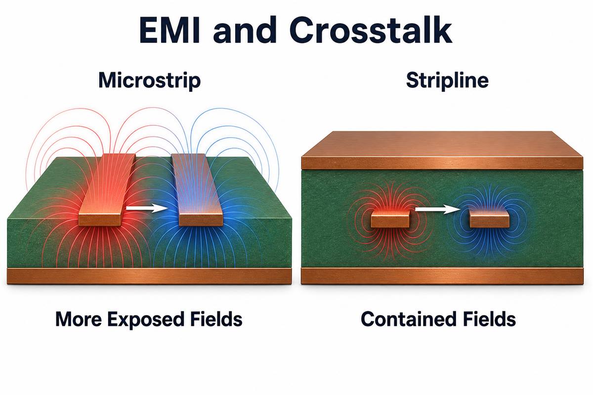
EMI and crosstalk field containment in microstrip and stripline routing

Microstrip can also achieve good signal integrity when it runs close to a continuous reference plane and maintains adequate separation from other nets. Problems increase near board edges, connectors, plane splits, apertures, or noisy switching nodes.

For both structures:

  • keep a continuous reference plane under or around the complete route;
  • increase spacing when parallel coupling is a concern;
  • avoid routing critical traces across plane splits and voids;
  • control return-current transitions near signal vias;
  • review connector launches and breakout regions, not only long straight traces.

Our guide to high-speed digital PCB design covers the wider relationship between stackup, crosstalk, reflection, via structures, and power integrity.

What Do Via Transitions and Return Paths Add?

A layer change adds a three-dimensional discontinuity that can outweigh the benefit of moving from microstrip to stripline. The signal via contributes inductance and capacitance, while unused via barrel can behave as a stub. The return current also needs a short path between reference planes.
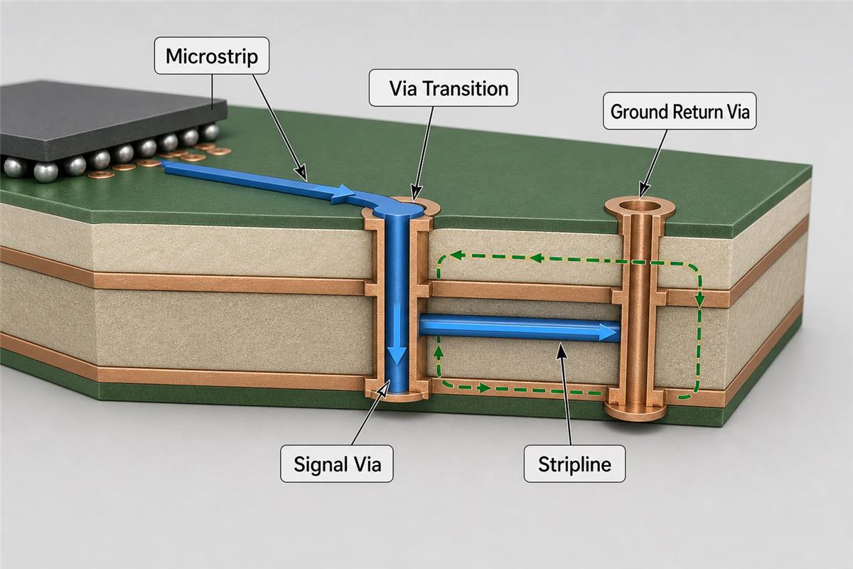
Microstrip to stripline signal via transition with a nearby ground return via

Place an appropriate ground return via close to a signal-via transition when both routing layers reference ground planes. If the reference changes between ground and power, provide a low-inductance return path that matches the interface and power-distribution design.

For thick boards or very high data rates, review residual stub length and consider whether blind vias or PCB backdrilling are justified. The right solution depends on channel bandwidth, board thickness, via diameter, breakout constraints, and cost.

When Should You Use Microstrip?

Use microstrip when direct access to surface components, probing, short routing, or fewer layer transitions matters more than maximum field containment. It is often practical for connector launches, short RF paths, test points, antennas, and surface-component fanout.

Microstrip is a strong candidate when:

  • the route can stay short and continuously referenced;
  • the design must avoid extra signal vias;
  • lab probing or tuning access is important;
  • the solder mask and final copper geometry are included in the impedance model;
  • adequate spacing from aggressors and board edges is available.

Do not choose it only because it appears simpler in a calculator. Surface plating, etching, solder mask, nearby components, and environmental exposure still affect the finished channel.

When Should You Use Stripline?

Use stripline when field containment, route-to-route isolation, or protected inner-layer routing is more valuable than probe access and via-free connection to surface components. It is often suitable for long internal routes, sensitive clocks, dense high-speed buses, and channels near noisy circuits.

Stripline is a strong candidate when:

  • the stackup can provide two continuous reference planes;
  • inner-layer line width and spacing remain manufacturable;
  • layer-transition vias and their return paths are designed as part of the channel;
  • the extra layer resources fit the board cost and thickness target;
  • finished dielectric thickness and layer registration can be controlled.

A practical 10-layer PCB stackup may use both microstrip and stripline layers so placement, breakout, isolation, and routing density can be balanced instead of forcing one topology across the whole board.

What Should Be Specified to the PCB Fabricator?

Controlled impedance should be agreed with the fabricator before layout is frozen. A trace width calculated from a nominal online stackup may change after the actual laminate, prepreg construction, finished copper, and producible etch geometry are selected.

Provide or confirm:

  • layer count, finished board thickness, and proposed stackup;
  • laminate family and frequency-relevant Dk and Df requirements;
  • single-ended and differential impedance targets with tolerances;
  • which layers use microstrip, embedded microstrip, or stripline;
  • finished copper weight, permitted line-width adjustment, and minimum spacing;
  • solder mask state over controlled microstrip traces;
  • coupon, TDR report, and any frequency-domain test requirement;
  • critical via structures, backdrill depth, and maximum residual stub if applicable.

Mark controlled-impedance nets and layers clearly in the fabrication drawing. Do not leave the manufacturer to infer which geometry or tolerance applies from Gerber files alone.

How Is Controlled Impedance Verified?

Controlled impedance is commonly verified with dedicated coupons built on the same production panel and measured by time-domain reflectometry. The coupon should represent the relevant layer, copper construction, dielectric thickness, and transmission-line geometry.
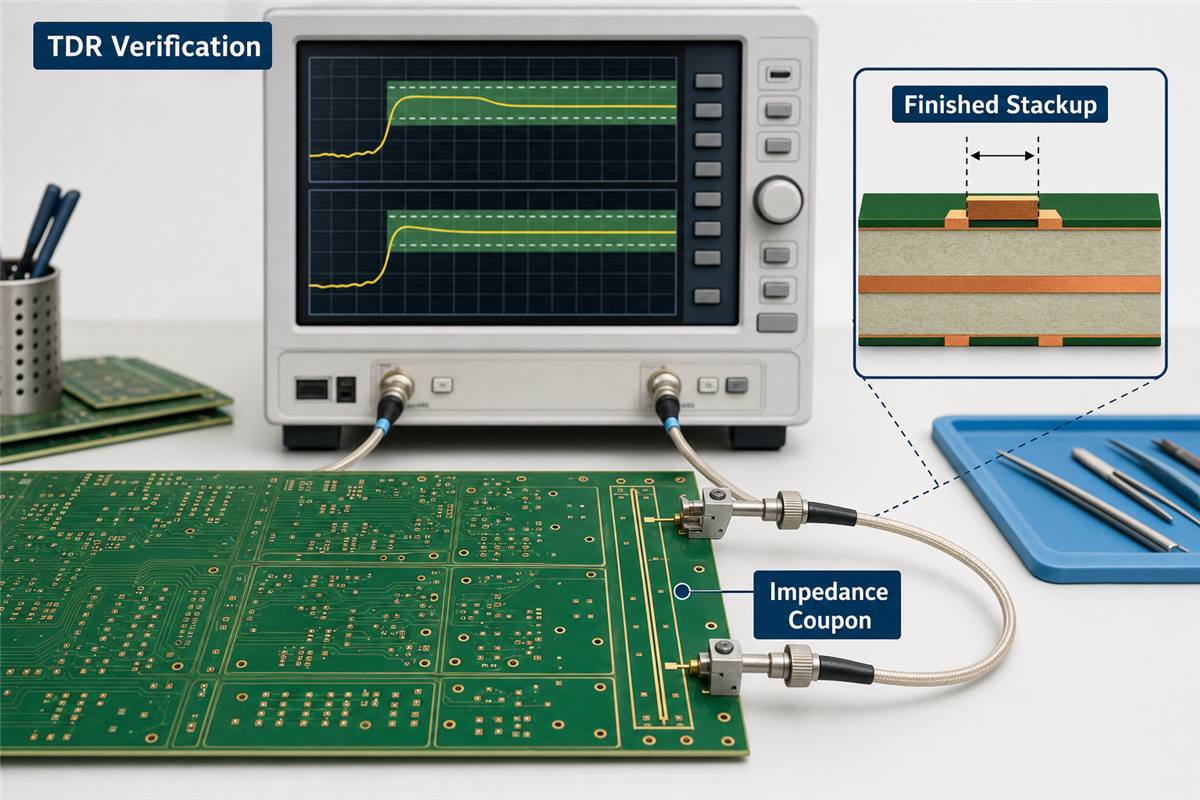
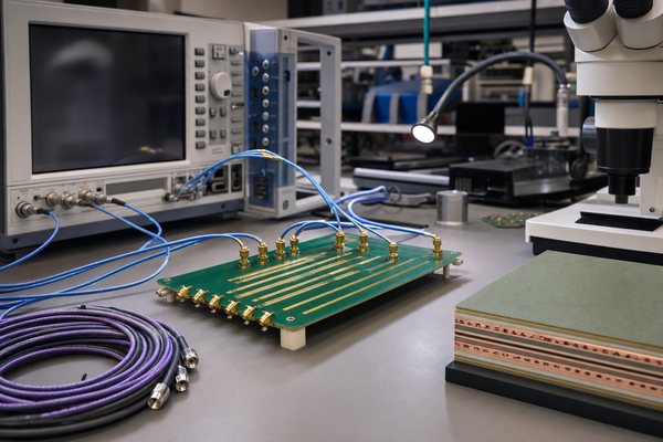
TDR verification of a controlled-impedance PCB coupon and finished stackup

Verification should connect design intent to the finished build:

  1. Confirm the released stackup and target geometries.
  2. Fabricate representative coupons with the production panel.
  3. Measure the coupon using the agreed TDR method.
  4. Compare the result with the specified target and tolerance.
  5. Record any approved line-width compensation for repeat builds.

A passing coupon does not automatically prove every channel is free from discontinuities. Connector launches, pads, neck-downs, plane crossings, and vias still require layout review or channel simulation. The broader PCB return-path guide explains why reference continuity remains important after nominal impedance is correct.

FAQ About Stripline and Microstrip

Is stripline always better than microstrip?

No. Stripline usually offers stronger field containment, while microstrip offers easier access and can avoid layer-transition vias. The better structure is the one that meets channel, stackup, manufacturing, test, and cost constraints with adequate margin.

Can stripline and microstrip have the same impedance?

Yes. Both can be designed for the same target impedance, but they normally require different trace widths, dielectric heights, and spacing. Each geometry must be calculated from its own finished stackup.

Does solder mask change microstrip impedance?

Yes. Solder mask changes the dielectric environment above a microstrip trace. Its thickness and Dk should be included when the required impedance tolerance or operating frequency makes the effect significant.

Is stripline always lower loss?

No. Stripline can reduce radiation and improve mode containment, but its field travels through dielectric and it may require lossy via transitions. Compare total insertion loss using the actual material, geometry, frequency, and channel length.

Can one differential pair change from microstrip to stripline?

Yes, but the transition needs a properly designed pair of signal vias, suitable antipads, controlled stubs, and nearby return paths. Keep the pair symmetrical and include the transition in simulation or validation when channel margin is limited.

How Can EBest Circuit Support Controlled-Impedance PCB Projects?

At EBest Circuit, we support controlled-impedance PCB projects by reviewing stackup, material, routing geometry, copper construction, via requirements, and inspection needs before fabrication. We can work with designs that combine surface microstrip and internal stripline when both structures are defined against the production stackup.

For a manufacturing review, send your Gerber or ODB++ data, fabrication drawing, layer stackup, impedance table, material requirement, board quantity, and any TDR or coupon requirement to sales@bestpcbs.com. We will review the data and clarify manufacturability before quotation.


You may also like

Stripline vs Microstrip: How to Choose for High-Speed PCB Routing?
Wednesday, July 29th, 2026

Choose microstrip when short surface routes, direct component access and easy probing matter most; choose stripline when stronger field containment and internal-layer isolation are the priority. Neither structure is automatically better or lower loss. The correct stripline vs microstrip decision depends on the production stackup, target impedance, frequency content, route length, copper profile, transition count and verification plan.

Stripline vs Microstrip title over a high-speed multilayer PCB engineering scene

For high-speed digital and RF engineers, the choice comes down to which geometry still meets impedance and channel targets after fabrication tolerances are applied. The sections below connect electromagnetic behavior with layout, manufacturing and test decisions so the selected trace can be built and verified, not merely drawn.

What Is Stripline vs Microstrip in PCB Design?

Microstrip is an outer-layer trace referenced mainly to one plane, while stripline is an internal trace routed between reference planes. Both are PCB transmission-line structures used when an interconnect is electrically long compared with the signal rise time or wavelength. At that point, trace geometry and the surrounding dielectric control characteristic impedance, propagation velocity and field behavior.

A surface microstrip usually has dielectric below the trace and air, solder mask or coating above it. Its fields therefore occupy more than one dielectric environment, making it a quasi-TEM structure with an effective dielectric constant below the laminate’s bulk Dk. A stripline is surrounded by PCB dielectric and bounded by planes, so its fields are more fully contained and its propagation is closer to transverse electromagnetic behavior.

Stripline vs Microstrip Stackup: How Do Their Structures Differ?

The structural difference is the trace’s position relative to dielectric and reference planes. Microstrip provides surface accessibility and a simple path to component pads. Stripline uses an internal signal layer and one plane on each side, which contains more of the electric field but requires vias to reach surface-mounted components.

Comparison Dimension Microstrip Stripline Design Consequence
Signal-layer position Outer layer Inner layer Microstrip reaches components directly; stripline needs transitions
Primary references Usually one nearby plane Planes above and below Stripline normally provides stronger field containment
Dielectric environment Mixed dielectric and air or coating Mostly PCB dielectric Microstrip uses effective Dk; stripline is governed more directly by laminate Dk
Probe access Direct Indirect Debugging an internal route may require coupons, pads or test structures
Fabrication inputs Core/prepreg, copper and solder mask Two dielectric separations, copper and plane geometry Both must use the actual pressed production stackup
Microstrip and stripline field distribution and containment

Symmetric stripline places the trace near the midpoint between two planes. Offset or asymmetric stripline moves it closer to one plane, changing impedance and coupling. A designer should not call every buried trace “stripline”: if the upper reference is missing, distant or interrupted, the return-current behavior may no longer match the assumed model.

Stripline vs Microstrip Impedance: What Controls Each Structure?

Impedance is controlled by the complete cross-section, not by trace width alone. For both structures, wider traces and smaller dielectric spacing generally reduce impedance, while narrower traces and larger spacing generally raise it. Copper thickness, etched sidewall shape, dielectric constant and nearby conductors also shift the result.

Microstrip impedance is sensitive to the substrate height below the trace, finished trace width, copper thickness, effective Dk and any solder mask covering. Stripline impedance depends on trace width and thickness, laminate Dk, and the distance to both reference planes. For differential pairs, spacing between the two conductors introduces odd-mode coupling, so a single-ended width calculation cannot establish differential impedance by itself.

Input Microstrip Effect Stripline Effect Production Check
Trace width Strong impedance control Strong impedance control Use finished top and bottom width after etching
Dielectric spacing Distance to the main reference plane Distance to both reference planes Use pressed thickness, not only nominal prepreg data
Dielectric constant Effective Dk includes the upper environment Bulk laminate Dk has greater influence Confirm frequency and test method for Dk values
Solder mask Can lower impedance by adding dielectric above the trace Normally no direct effect on an internal trace Include mask thickness and coverage in the model when relevant
Adjacent copper Ground coplanar features may add coupling Nearby routes and plane openings disturb fields Model the actual clearance and anti-pad geometry

A 50-ohm microstrip width should never be copied directly to a stripline layer and assumed to remain 50 ohms. The layer geometry is different, and the required stripline width may change substantially. Freeze the material construction and finished copper assumptions with the PCB manufacturer before final length tuning.

Why Do Microstrip and Stripline Have Different Propagation Delays?

Stripline is usually slower because its field propagates through more dielectric, while part of a microstrip field travels through air or coating above the board. Propagation delay is approximately proportional to the square root of the effective relative permittivity. The relevant value for microstrip is effective Dk; for stripline it is closer to the laminate Dk seen by the field.

For a first-pass estimate, use approximately 84.7 × √Dk ps/in for a homogeneous TEM line. A stripline behaving near Dk 4, for example, would be close to 169 ps/in. Microstrip on the same laminate has a lower effective Dk and therefore a shorter delay per inch. Treat these as preliminary values, not production acceptance limits, because resin content, glass style, frequency, copper roughness and geometry change the result.

Delay matters when matching clocks, memory buses, serial links and differential-pair members. Length matching by geometry alone can be misleading if two routes occupy different transmission-line environments. When a channel changes from microstrip to stripline, calculate electrical delay for each segment and include the vias and package transitions instead of matching only total routed length.

Stripline vs Microstrip Loss: Which Has Lower Insertion Loss?

Neither geometry is always lower loss; total insertion loss depends on conductor, dielectric, radiation and transition losses across the required frequency range. Stripline limits radiation but often uses a narrower trace for a target impedance and keeps the field inside dielectric, which can increase conductor and dielectric loss. Microstrip can use a wider conductor and place part of its field in air, yet it may radiate more and can suffer from solder-mask and surface-roughness effects.

Loss Component Microstrip Stripline Primary Control
Conductor loss Depends on width, thickness and surface profile Can rise when the required trace is narrower Finished geometry, copper roughness and skin effect
Dielectric loss Part of the field may travel outside the laminate More field energy remains in the dielectric Material Df, frequency and route length
Radiation loss Generally higher, especially near discontinuities Generally lower because of plane containment Reference continuity, geometry and transitions
Transition loss Low for direct surface launches May require more vias and stubs Via length, anti-pad, return vias and launch design

Compare loss with a channel model that uses the proposed laminate’s Dk and Df at a relevant frequency, a realistic copper profile and the complete transition count. For long high-speed channels, review insertion loss as S21 over frequency instead of reducing the result to a single “better” label. Select the structure that meets the channel budget without sacrificing EMI margin, routing density or manufacturability.

How Do Microstrip and Stripline Affect Crosstalk, EMI and Bandwidth?

Stripline normally offers better field containment, but spacing, coupled length and reference continuity can matter more than the layer name. A tightly packed stripline bundle can still exhibit unacceptable crosstalk, while a well-spaced microstrip with an uninterrupted plane can perform cleanly. EMI and crosstalk must therefore be evaluated from geometry and return-current paths.

Microstrip fields extend farther into the region above the board, increasing exposure to neighboring conductors, connectors, enclosures and external noise. Stripline fields terminate mainly on the adjacent planes, reducing radiation and susceptibility. However, a plane split, void, poorly placed stitching via or oversized anti-pad can force return current to detour and create a larger loop that undermines the expected benefit.

Usable bandwidth is not fixed by choosing microstrip or stripline. It is limited by frequency-dependent loss, dispersion, impedance discontinuities, resonant stubs, connector launches and receiver margin. Microstrip has greater dielectric inhomogeneity and can exhibit more dispersion, while stripline may accumulate more dielectric loss. Simulate the complete channel to the highest significant spectral content rather than using only the clock frequency or data rate.

How Does Differential Pair Routing Differ Between Stripline and Microstrip?

Differential pairs in both structures require controlled odd-mode coupling, but stripline adds stronger dependence on plane symmetry and the spacing to two references. Microstrip pairs are easier to probe and launch from surface components. Stripline pairs provide stronger containment but require carefully designed layer transitions.

  • Pair geometry: Solve trace width, intra-pair gap, copper thickness and dielectric spacing together for the target differential impedance.
  • Plane symmetry: Keep stripline pairs consistently positioned between their reference planes unless an asymmetric construction has been modeled.
  • Skew control: Match electrical delay, not only routed length, when pair members cross glass-weave regions or different layer environments.
  • Coupled length: Maintain intended pair coupling while controlling spacing to unrelated aggressor traces.
  • Layer transitions: Route both members through comparable vias and place return vias symmetrically to limit mode conversion.

Do not tune a differential pair with excessive serpentine segments in a confined area. Closely spaced turns can couple to each other, changing the intended delay and impedance. If tuning is necessary, use solver-informed spacing and place the correction where the reference environment remains continuous.

What Are the Pros and Cons of Stripline vs Microstrip?

Microstrip favors accessibility and simple launches; stripline favors isolation and field containment. Apply the following trade-offs to the actual stackup instead of treating them as a universal ranking.

Decision Dimension Microstrip Stripline Preferred Condition
Component launch Direct and short Requires a via transition Microstrip for short surface escapes
Debug access Easy to probe Limited without test features Microstrip for development and tuning access
Field containment Lower Higher Stripline for dense or EMI-sensitive internal routing
Route isolation Requires disciplined spacing Benefits from adjacent planes Stripline when plane continuity is assured
Transition count Can remain on the surface Often adds vias Use the option with the cleaner end-to-end channel
Loss outcome Potentially wider trace and less dielectric participation Lower radiation but potentially higher dielectric participation Choose from modeled insertion loss, not a rule of thumb

Many successful multilayer boards use both. A route can begin as microstrip at a BGA escape or connector launch, transition to stripline for the long internal segment, and return to microstrip near the destination. This hybrid approach is effective only when the transitions, return paths and accumulated discontinuities are included in the channel analysis.

How Do Solder Mask, Copper Roughness and Fabrication Tolerances Affect Performance?

Fabrication details can shift impedance and loss enough to invalidate a nominal calculator result. The production model should use finished geometry, the selected material construction and realistic process tolerances rather than ideal CAD dimensions.

  • Solder mask: A dielectric coating above microstrip increases effective permittivity and generally lowers impedance; the effect depends on thickness, coverage and frequency.
  • Copper roughness: Rough copper increases the effective current path and conductor loss as skin depth decreases with frequency.
  • Etch shape: A trapezoidal finished trace has different top and bottom widths, so impedance should not be modeled from nominal artwork width alone.
  • Pressed dielectric: Prepreg thickness changes during lamination according to resin content, copper distribution and process conditions.
  • Material Dk: Datasheet values depend on test method and frequency and may not equal the design Dk used by a field solver.
  • Registration: Layer-to-layer offset can change spacing to nearby copper and disturb tightly coupled differential geometry.

Before routing is frozen, request a proposed production stackup and confirm which dimensions the manufacturer will adjust to meet impedance. A clear impedance table should identify layer, net type, target impedance, tolerance, reference plane, nominal width and gap. This prevents an uncontrolled last-minute width change from affecting routing clearance or pair coupling.

How Should Microstrip-to-Stripline Via Transitions and Return Paths Be Designed?

A layer transition must provide both a low-discontinuity signal path and a nearby path for return current to change reference planes. Treat the signal via, anti-pad, unused stub and return vias as one electromagnetic structure.

  1. Identify the reference plane used by the incoming microstrip and the planes that bound the destination stripline.
  2. Place ground return vias close to the signal transition so return current does not travel around a large plane opening.
  3. Keep differential-pair signal vias and return vias geometrically balanced to reduce common-mode conversion.
  4. Optimize the via pad, anti-pad and capture-pad geometry with a 3D model when data rate or channel margin justifies it.
  5. Reduce an electrically significant unused via stub by selecting an appropriate layer transition or considering backdrilling.
  6. Avoid routing the transition through plane splits, voids, dense anti-pad clusters or poorly referenced connector regions.
  7. Include the connector, package breakout and every layer change in the final channel simulation.

There is no reliable universal rule for return-via quantity or spacing. Minimize loop area and maintain a continuous reference transition over the signal’s relevant spectrum. For differential channels, inspect both differential insertion loss and mode conversion; equal-looking vias do not guarantee electrical balance.

How Should Stripline and Microstrip Impedance Be Calculated, Simulated and Verified?

Use equations for an initial estimate, a field solver for the production cross-section and measurements to verify the fabricated result. No single tool covers geometry definition, process variation and physical acceptance by itself.

  1. Define the target single-ended or differential impedance and the allowed tolerance from the interface requirement.
  2. Obtain the proposed laminate family, layer construction, finished copper and pressed dielectric dimensions.
  3. Use a closed-form calculator to establish a practical starting width and spacing.
  4. Build the actual microstrip or stripline cross-section in a 2D field solver, including solder mask and trapezoidal copper where relevant.
  5. Run a tolerance sweep for dielectric thickness, Dk, finished width, copper thickness and pair gap.
  6. Use a 3D solver for vias, launches, connectors, plane changes and other discontinuities that a 2D cross-section cannot represent.
  7. Release an impedance table that links each target to a specific layer, reference and geometry.
  8. Fabricate an impedance coupon with the same layer construction and process conditions as the board.
  9. Measure the coupon with TDR and correlate failures with microsection dimensions when necessary.
  10. Use VNA S-parameters for insertion loss, return loss and mode conversion when the channel specification requires frequency-domain evidence.
Stripline and microstrip impedance verification with TDR and VNA equipment

TDR shows impedance versus time or distance but does not, by itself, prove that an entire assembled link meets its insertion-loss budget. A microsection confirms physical dimensions at a sampled location but does not measure every electrical discontinuity. VNA data reveals frequency-domain behavior but requires suitable fixtures, calibration and de-embedding. Use the measurements together according to the acceptance question.

When Is Coplanar Waveguide Better Than Microstrip or Stripline?

Grounded coplanar waveguide can be preferable when a surface RF route needs lateral ground control, compact launches or convenient grounding around components. It places ground copper beside the signal trace and normally uses a reference plane below, creating a geometry controlled by trace width, side gap, substrate height and ground-via arrangement.

CPW works well around RF connectors, filters, matching networks and exposed measurement points where surface grounding and launch shaping matter. It is not automatically superior: tight side gaps may challenge etching capability, sparse ground vias can allow unwanted modes, and nearby ground copper changes impedance. Model the actual side clearance and via fence.

Use microstrip for a simple surface route when lateral ground is unnecessary. Use stripline for a long internal route requiring greater containment. Evaluate grounded CPW as a separate option when the surface launch, component grounding or isolation requirement justifies its extra geometry and fabrication controls.

When Should You Use Stripline vs Microstrip for High-Speed PCB Routing?

Start with the dominant system constraint, then verify the decision against the complete channel. Many boards use microstrip for short launches and stripline for longer internal routing instead of forcing one geometry everywhere.

  1. Choose microstrip first when the route is short, remains near surface components, needs probing or must avoid extra vias.
  2. Choose stripline first when routing density, isolation, crosstalk control or radiated-emission margin dominates.
  3. Compare modeled insertion loss using the selected laminate, realistic copper roughness and the actual route length.
  4. Count every transition and determine whether its via stub and return path consume more margin than the preferred routing layer saves.
  5. Confirm that the fabricator can hold the required geometry and impedance tolerance on the proposed stackup.
  6. Define coupon, TDR and optional S-parameter acceptance before releasing production data.

For an RF launch or a short clock route, accessible microstrip may be the cleanest solution. For a dense serial backplane channel or a timing-critical bus surrounded by aggressors, stripline may provide valuable isolation. The final choice should be recorded in the stackup and impedance table so layout, simulation, fabrication and inspection use the same geometry.

What Are the Most Common Questions About Stripline vs Microstrip?

These supplementary answers address practical questions that arise after the main geometry has been selected.

Q1: Can a power plane serve as the reference for a high-speed transmission line?

A1: Yes, if the power plane is continuous and provides a sufficiently low-impedance return path over the signal spectrum. The return current may need nearby decoupling capacitors when a transition changes between power and ground references. Do not route across power-plane splits or isolated islands, because the resulting return-path detour increases loop area and discontinuity.

Q2: Do rounded corners improve stripline or microstrip performance?

A2: Rounded corners are rarely the primary performance control for ordinary digital routing. A well-designed 45-degree bend is generally more practical than an abrupt 90-degree corner, but the effect depends on width and frequency. Reference continuity and transition geometry usually matter more. Very high-frequency RF bends may require mitering or electromagnetic optimization.

Q3: Can guard traces reduce crosstalk beside a microstrip route?

A3: A grounded guard trace can help only when it is connected to the reference plane with an appropriate via pattern and does not create a resonant floating conductor. It also consumes routing space and changes the local field geometry. Increasing separation is often the cleaner first action; simulate the guard structure when spacing alone cannot satisfy coupling limits.

Q4: How does glass weave affect differential stripline and microstrip pairs?

A4: The two conductors can encounter different local resin and glass environments, creating unequal effective permittivity and differential skew. The risk grows with longer routes, finer geometry and faster edges. Use weave-aware routing when the timing margin is small, such as routing at an angle, selecting a spread-glass construction or working with the fabricator on laminate style.

Q5: Is broadside differential stripline equivalent to edge-coupled stripline?

A5: No. Edge-coupled pairs place both conductors on one layer, while broadside pairs place them on adjacent layers. Broadside geometry is more sensitive to layer registration and dielectric thickness between the pair. Model broadside coupling as its own structure; do not reuse the width and gap from an edge-coupled differential pair.

Q6: Does copper plating affect controlled-impedance traces?

A6: It can. Outer-layer traces may gain copper during plating, changing finished thickness and etched shape, while inner-layer traces follow a different process path. The impedance model should therefore use finished conductor geometry supplied or approved by the fabricator. Distinguish base copper from finished copper in the stackup and impedance documentation.

Q7: How does temperature affect propagation delay and impedance?

A7: Temperature can change dielectric properties and physical dimensions, so both delay and impedance may shift. The significance depends on laminate characteristics, temperature range and system margin. Use temperature-dependent material data for critical environments, and validate the complete channel when automotive, aerospace, power or outdoor operation creates a wide thermal range.

Q8: Can a chassis or enclosure replace the PCB reference plane?

A8: Not for normal controlled-impedance routing. A distant chassis does not provide the same tightly coupled return path as an adjacent solid PCB plane. It may influence common-mode radiation and shielding, but it should not be treated as the primary transmission-line reference. Keep the intended reference plane continuous beneath or around the route.

Q9: Should unused copper be removed near stripline and microstrip routes?

A9: Copper pours can remain if their clearance, reference connection and effect on impedance are defined. Floating or inconsistently spaced copper can change local coupling and create resonances. Apply a controlled keepout or intentionally grounded copper rule rather than allowing automatic pours on production artwork to approach a critical route unpredictably.

Q10: How should impedance tolerance be selected for a new PCB?

A10: Start with the interface requirement and channel sensitivity, then confirm what the proposed stackup and fabrication process can hold. A tighter tolerance may require more coupon control, engineering adjustment and cost without improving system performance. Specify the widest tolerance that still protects link margin, and agree on the measurement method before production.

Stripline and microstrip are engineering options, not competing quality grades. Select the structure that meets impedance, loss, timing, EMI, density and test-access requirements with the strongest fabrication margin. Freeze the production stackup, model transitions and define measurement evidence before final routing.

If you are looking for reliable OEM manufacturing, ODM production, prototype development, mass production or custom engineering solutions, contact EBest Circuit. Send your Gerber/ODB++, BOM, quantity, stackup, impedance targets, assembly requirements and test plan to sales@bestpcbs.com for engineering review and a quotation.

You may also like