Stripline vs microstrip is a choice between an inner-layer transmission line surrounded by dielectric and an outer-layer transmission line exposed to air and solder mask. Stripline provides stronger field containment and isolation. Microstrip usually gives easier probing, direct access to surface components, and fewer layer-transition vias.
Neither structure is automatically better. The right choice depends on the target impedance, frequency or edge rate, channel length, loss budget, EMI risk, layer count, via transitions, routing density, and manufacturing tolerance. This guide compares those tradeoffs and shows what engineers should define before releasing controlled-impedance PCB data.
What Is the Difference Between Stripline and Microstrip?
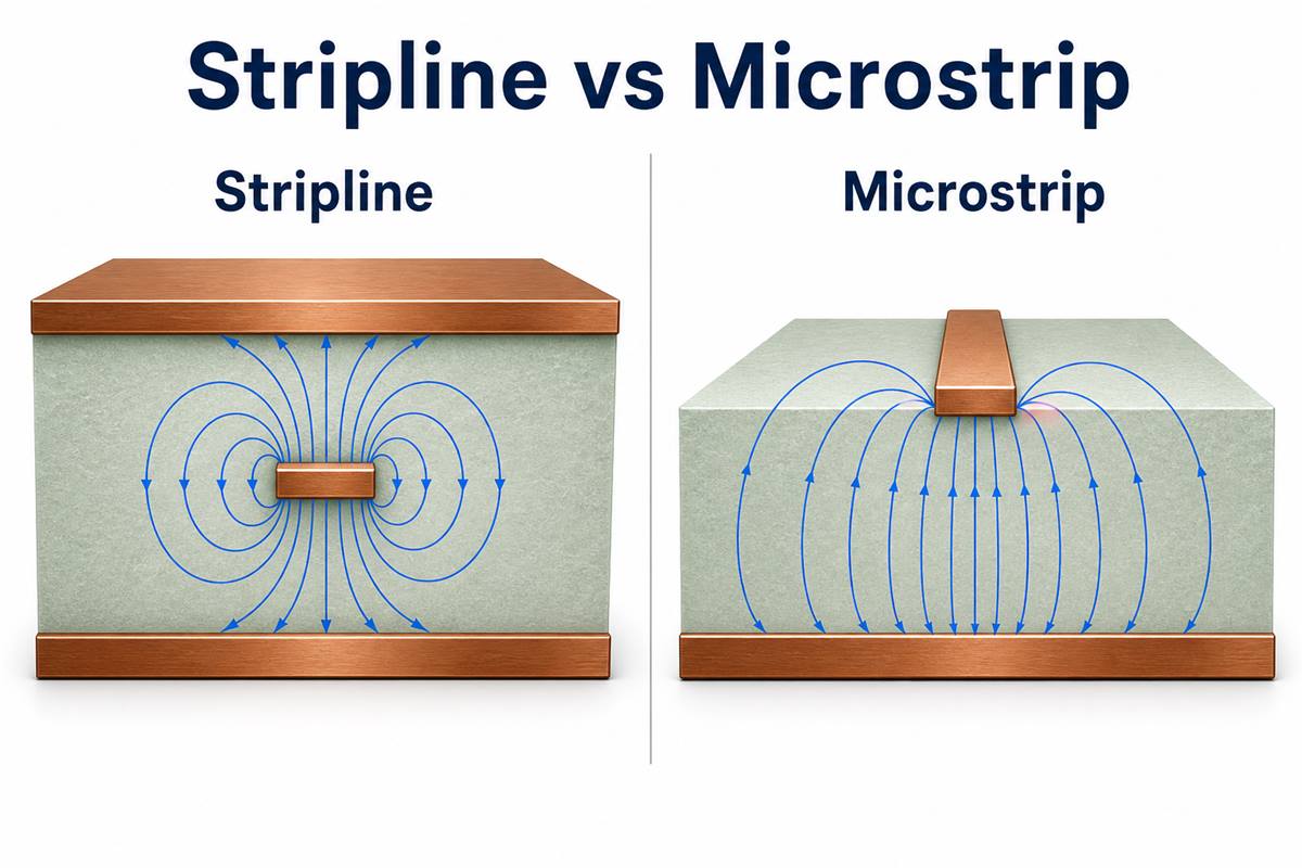
Microstrip is a surface trace referenced mainly to one adjacent plane, while stripline is an internal trace embedded between two reference planes. This placement changes the electromagnetic field, effective dielectric constant, propagation delay, coupling, probing access, and the number of vias needed to reach components.
- Microstrip: The trace sits on an outer copper layer. Part of its field travels through PCB dielectric and part through air or solder mask, so it behaves as a quasi-TEM transmission line.
- Stripline: The trace is surrounded by dielectric between two planes. Its field is more tightly contained, and a symmetric structure can approximate a TEM transmission line.
- Embedded microstrip: A covered outer-layer-like trace under a dielectric layer is not the same as a true stripline. Its field and impedance must be modeled with the actual stackup.
- Asymmetric stripline: The trace is not centered between its reference planes. Different dielectric heights above and below the trace change its impedance and coupling.
A PCB can use both structures. For example, a short route from a surface BGA pad may begin as microstrip and then change to stripline for a longer, better-contained channel. The transition itself must be included in the channel design.
Stripline vs Microstrip Pros and Cons
The practical differences are field containment, accessibility, propagation environment, layer usage, and transition cost. The table compares the two structures without assuming the same trace width or dielectric spacing.
| Design Factor | Microstrip | Stripline |
|---|---|---|
| Trace location | Outer PCB layer | Inner PCB layer between two planes |
| Field containment | Partly exposed above the board | Mostly contained inside dielectric |
| Component access | Direct route to surface pads | Normally requires a via transition |
| Probing and rework | Easier to access | Hidden after lamination |
| Layer resources | Uses an outer signal layer and one nearby plane | Uses an inner signal layer bounded by two planes |
| Environmental sensitivity | Affected by solder mask and material above the trace | More stable when the internal dielectric structure is controlled |
| Isolation | More exposed to neighboring fields | Usually better field containment and isolation |
These are tendencies, not universal performance guarantees. A carefully designed microstrip can outperform a poorly designed stripline channel. Trace length, spacing, material loss, copper roughness, plane continuity, and via geometry still control the result.
The final stripline vs microstrip decision should therefore be based on the complete channel and the producible stackup, not on one isolated advantage.
How Does Stripline vs Microstrip Impedance Differ?
Stripline vs microstrip impedance differs because the electromagnetic field sees different dielectric environments and reference-plane geometry. Neither structure has a fixed characteristic impedance; both must be calculated from the finished production stackup.
Important single-ended impedance inputs include:
- finished trace width and copper thickness;
- dielectric height to the reference plane or planes;
- material Dk at the relevant frequency;
- etch shape and conductor sidewall profile;
- solder mask thickness and Dk for microstrip;
- surface copper plating and final finish;
- whether the stripline is symmetric or asymmetric.
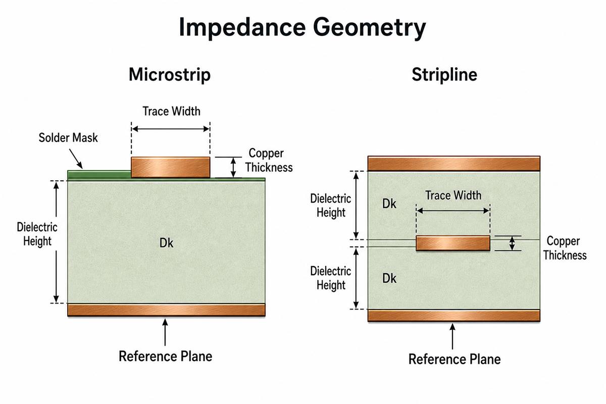
For the same target impedance, the required line width can differ substantially between structures. Copying a microstrip width onto an inner stripline layer will not preserve impedance. Start with the fabricator’s proposed stackup, calculate each geometry separately, and then confirm the producible width and spacing.
Which Structure Has Lower Transmission Loss?
There is no universal winner for stripline vs microstrip loss. Stripline keeps its field inside the dielectric and may experience more dielectric loss, while microstrip can suffer more radiation, surface-condition sensitivity, and conductor-related effects. The total channel loss depends on the actual geometry and materials.
Evaluate the following loss mechanisms together:
- Dielectric loss: Driven by material Df, frequency, field distribution, and route length.
- Conductor loss: Influenced by finished copper cross-section, skin effect, and copper roughness.
- Radiation loss: More relevant when fields are less contained or reference paths are disrupted.
- Discontinuity loss: Added by vias, pads, connectors, neck-downs, stubs, and plane transitions.
Do not compare loss using the same line width alone. A fair comparison holds the target impedance and material system constant, then optimizes the geometry of each structure. Long multi-gigabit or RF channels may require field-solver modeling and insertion-loss simulation rather than a simple closed-form calculator.
How Does Propagation Delay Differ?
Stripline is generally slower than microstrip of the same physical length because its field propagates through the PCB dielectric, while part of a microstrip field travels through air or solder mask with a lower effective permittivity. The exact propagation delay microstrip vs stripline relationship depends on stackup geometry and material Dk.
This difference matters when timing is compared across routes. Two traces with equal physical length can have different electrical delay if one is microstrip and the other is stripline. For clocks, source-synchronous buses, matched RF paths, and multi-lane SerDes:
- keep matched members on the same transmission-line structure where possible;
- match electrical delay, not only CAD length;
- include package, connector, via, and layer-transition delay;
- use the laminate’s frequency-dependent Dk rather than a generic FR-4 value when timing margin is tight.
The same principle applies when interpreting an eye diagram: additional skew, attenuation, and reflections can reduce eye width and eye height even when the nominal route lengths appear matched.
How Do Differential Pairs Behave in Each Structure?
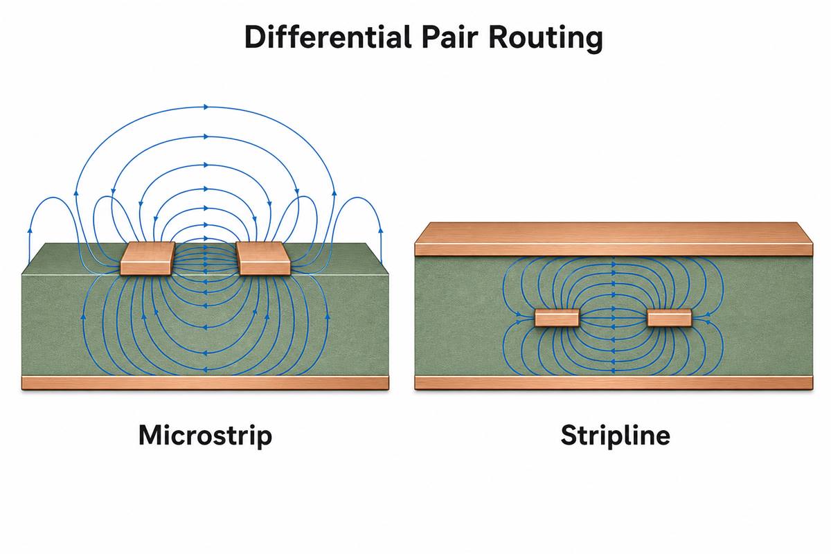
Differential pair stripline vs microstrip requires comparing both the trace-to-plane coupling and the coupling between the two traces. Pair spacing, line width, dielectric height, copper thickness, and reference geometry determine the differential impedance and odd-mode behavior.
Microstrip pairs are accessible and can route directly from surface pads, but their fields are less confined and solder mask affects impedance. Stripline pairs are better contained, but their required widths and spacing must fit the inner-layer design rules. Broadside-coupled stripline is another option, yet layer registration becomes a critical manufacturing variable.
Good differential routing practice includes:
- using one approved geometry for the critical part of the pair;
- keeping both traces on the same layer and reference structure;
- avoiding unnecessary uncoupling around pads and vias;
- minimizing pair skew without adding excessive serpentine coupling;
- defining both the differential target and any single-ended constraint required by the interface.
Which Structure Controls EMI and Crosstalk Better?
Stripline generally provides better field containment because the signal trace is bounded by two reference planes. That can reduce emissions and coupling to other circuits, but it does not correct poor spacing, plane voids, long parallel routes, or a badly designed via transition.
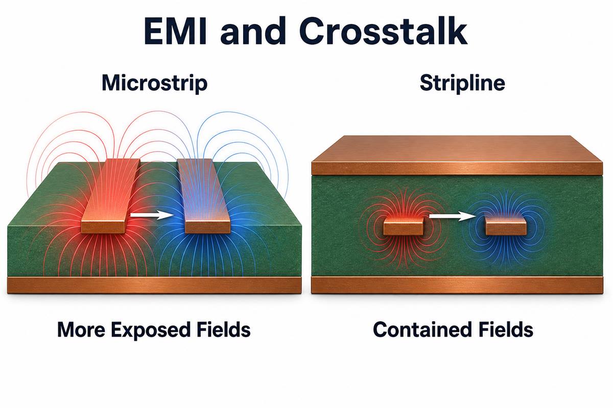
Microstrip can also achieve good signal integrity when it runs close to a continuous reference plane and maintains adequate separation from other nets. Problems increase near board edges, connectors, plane splits, apertures, or noisy switching nodes.
For both structures:
- keep a continuous reference plane under or around the complete route;
- increase spacing when parallel coupling is a concern;
- avoid routing critical traces across plane splits and voids;
- control return-current transitions near signal vias;
- review connector launches and breakout regions, not only long straight traces.
Our guide to high-speed digital PCB design covers the wider relationship between stackup, crosstalk, reflection, via structures, and power integrity.
What Do Via Transitions and Return Paths Add?
A layer change adds a three-dimensional discontinuity that can outweigh the benefit of moving from microstrip to stripline. The signal via contributes inductance and capacitance, while unused via barrel can behave as a stub. The return current also needs a short path between reference planes.
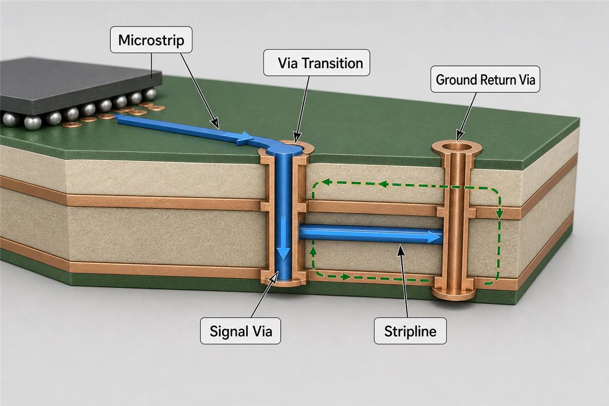
Place an appropriate ground return via close to a signal-via transition when both routing layers reference ground planes. If the reference changes between ground and power, provide a low-inductance return path that matches the interface and power-distribution design.
For thick boards or very high data rates, review residual stub length and consider whether blind vias or PCB backdrilling are justified. The right solution depends on channel bandwidth, board thickness, via diameter, breakout constraints, and cost.
When Should You Use Microstrip?
Use microstrip when direct access to surface components, probing, short routing, or fewer layer transitions matters more than maximum field containment. It is often practical for connector launches, short RF paths, test points, antennas, and surface-component fanout.
Microstrip is a strong candidate when:
- the route can stay short and continuously referenced;
- the design must avoid extra signal vias;
- lab probing or tuning access is important;
- the solder mask and final copper geometry are included in the impedance model;
- adequate spacing from aggressors and board edges is available.
Do not choose it only because it appears simpler in a calculator. Surface plating, etching, solder mask, nearby components, and environmental exposure still affect the finished channel.
When Should You Use Stripline?
Use stripline when field containment, route-to-route isolation, or protected inner-layer routing is more valuable than probe access and via-free connection to surface components. It is often suitable for long internal routes, sensitive clocks, dense high-speed buses, and channels near noisy circuits.
Stripline is a strong candidate when:
- the stackup can provide two continuous reference planes;
- inner-layer line width and spacing remain manufacturable;
- layer-transition vias and their return paths are designed as part of the channel;
- the extra layer resources fit the board cost and thickness target;
- finished dielectric thickness and layer registration can be controlled.
A practical 10-layer PCB stackup may use both microstrip and stripline layers so placement, breakout, isolation, and routing density can be balanced instead of forcing one topology across the whole board.
What Should Be Specified to the PCB Fabricator?
Controlled impedance should be agreed with the fabricator before layout is frozen. A trace width calculated from a nominal online stackup may change after the actual laminate, prepreg construction, finished copper, and producible etch geometry are selected.
Provide or confirm:
- layer count, finished board thickness, and proposed stackup;
- laminate family and frequency-relevant Dk and Df requirements;
- single-ended and differential impedance targets with tolerances;
- which layers use microstrip, embedded microstrip, or stripline;
- finished copper weight, permitted line-width adjustment, and minimum spacing;
- solder mask state over controlled microstrip traces;
- coupon, TDR report, and any frequency-domain test requirement;
- critical via structures, backdrill depth, and maximum residual stub if applicable.
Mark controlled-impedance nets and layers clearly in the fabrication drawing. Do not leave the manufacturer to infer which geometry or tolerance applies from Gerber files alone.
How Is Controlled Impedance Verified?
Controlled impedance is commonly verified with dedicated coupons built on the same production panel and measured by time-domain reflectometry. The coupon should represent the relevant layer, copper construction, dielectric thickness, and transmission-line geometry.
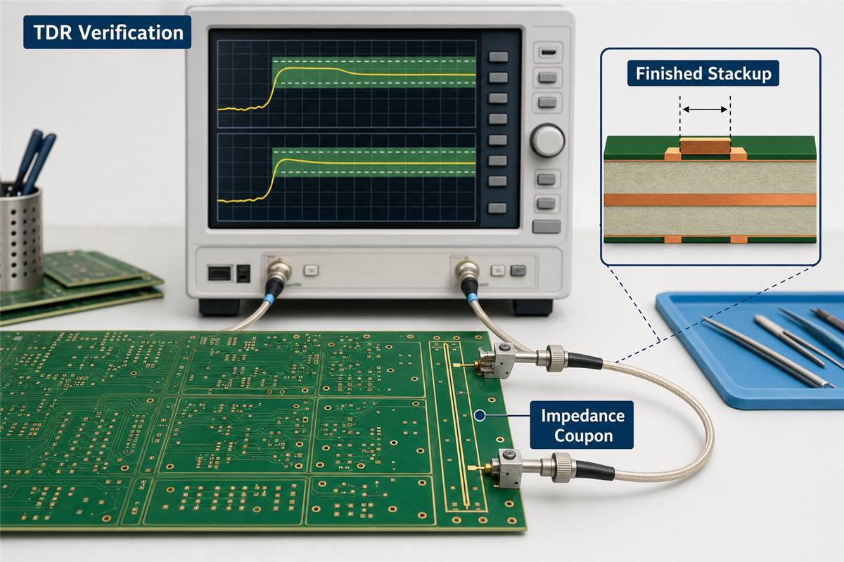
Verification should connect design intent to the finished build:
- Confirm the released stackup and target geometries.
- Fabricate representative coupons with the production panel.
- Measure the coupon using the agreed TDR method.
- Compare the result with the specified target and tolerance.
- Record any approved line-width compensation for repeat builds.
A passing coupon does not automatically prove every channel is free from discontinuities. Connector launches, pads, neck-downs, plane crossings, and vias still require layout review or channel simulation. The broader PCB return-path guide explains why reference continuity remains important after nominal impedance is correct.
FAQ About Stripline and Microstrip
Is stripline always better than microstrip?
No. Stripline usually offers stronger field containment, while microstrip offers easier access and can avoid layer-transition vias. The better structure is the one that meets channel, stackup, manufacturing, test, and cost constraints with adequate margin.
Can stripline and microstrip have the same impedance?
Yes. Both can be designed for the same target impedance, but they normally require different trace widths, dielectric heights, and spacing. Each geometry must be calculated from its own finished stackup.
Does solder mask change microstrip impedance?
Yes. Solder mask changes the dielectric environment above a microstrip trace. Its thickness and Dk should be included when the required impedance tolerance or operating frequency makes the effect significant.
Is stripline always lower loss?
No. Stripline can reduce radiation and improve mode containment, but its field travels through dielectric and it may require lossy via transitions. Compare total insertion loss using the actual material, geometry, frequency, and channel length.
Can one differential pair change from microstrip to stripline?
Yes, but the transition needs a properly designed pair of signal vias, suitable antipads, controlled stubs, and nearby return paths. Keep the pair symmetrical and include the transition in simulation or validation when channel margin is limited.
How Can EBest Circuit Support Controlled-Impedance PCB Projects?
At EBest Circuit, we support controlled-impedance PCB projects by reviewing stackup, material, routing geometry, copper construction, via requirements, and inspection needs before fabrication. We can work with designs that combine surface microstrip and internal stripline when both structures are defined against the production stackup.
For a manufacturing review, send your Gerber or ODB++ data, fabrication drawing, layer stackup, impedance table, material requirement, board quantity, and any TDR or coupon requirement to sales@bestpcbs.com. We will review the data and clarify manufacturability before quotation.