PCB manufacturing PCB manufacturing
Home > Blog

PCB Button Manufacturing Guide for Reliable PCB Assembly

August 3rd, 2026

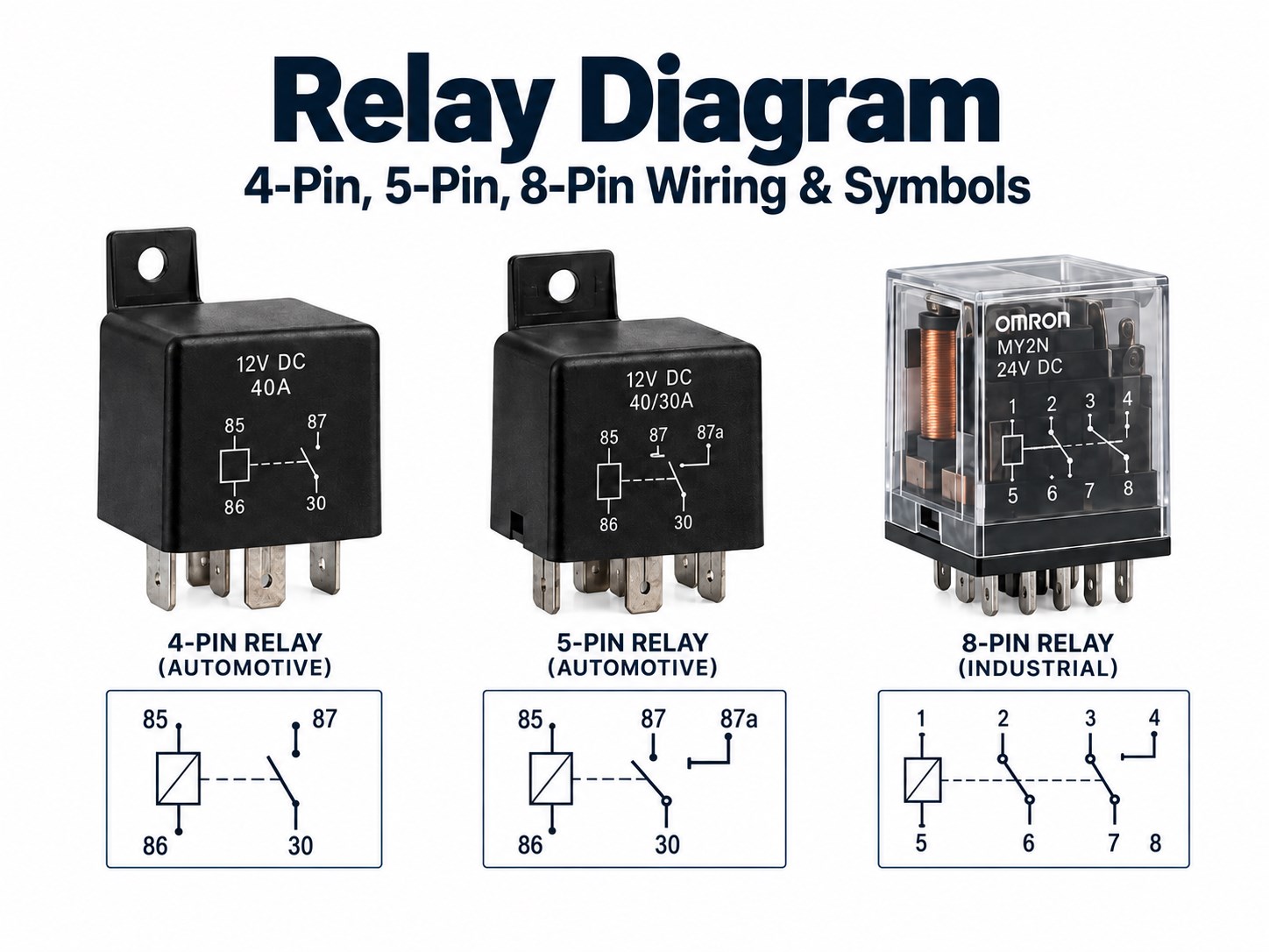
PCB button is a small input structure on a printed circuit board, but it can decide whether a product feels reliable, passes assembly smoothly, or creates repeated field complaints. In real manufacturing projects, “PCB button” may refer to a tactile switch soldered to a PCB, a metal dome contact pad, a push button switch mounted through the board, or a custom keypad area built into the board design.

For engineers and buyers, the key question is not only what the button does electrically. The bigger production question is whether the PCB footprint, surface finish, enclosure height, soldering method, inspection plan, and test method are clear before the order moves into fabrication and assembly.

EBest Circuit (Best Technology) supports customized PCB fabrication, PCB layout manufacturability review, component sourcing coordination, PCBA assembly, inspection, and testing support for button PCB projects used in control panels, handheld devices, industrial equipment, medical electronics, consumer products, and smart hardware. If your project includes PCB button structures or push-button switch assembly, you can contact sales@bestpcbs.com for engineering review before production.

PCB button
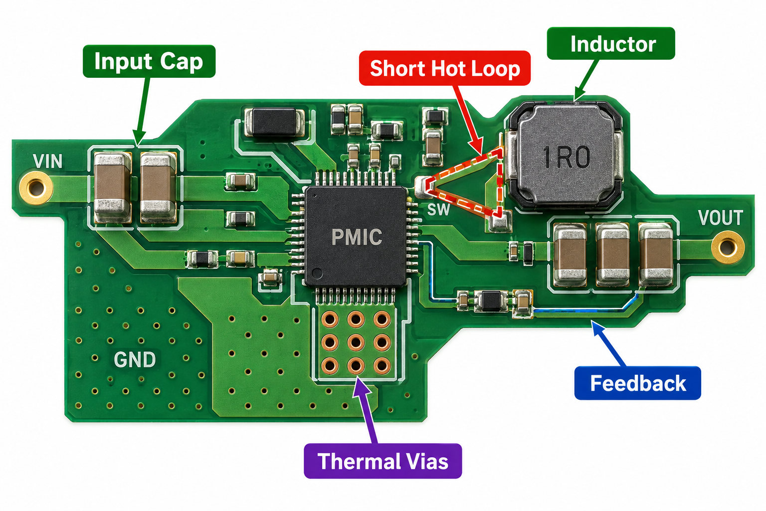
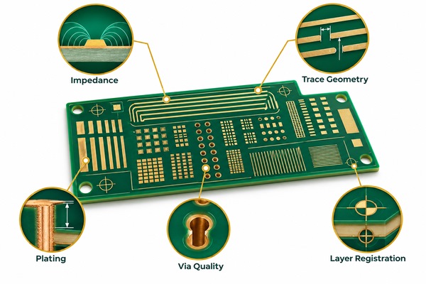
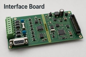
PCB button projects should be reviewed as PCB fabrication, component fit, assembly quality, and final product usability.

What Is a PCB Button?

A PCB button is a button function built on or mounted to a printed circuit board. It allows a user to press a physical area or switch and send an electrical signal to the circuit.

In real products, a PCB button can appear in several forms:

  • A tactile switch soldered by SMT or through-hole assembly
  • A metal dome placed over PCB contact pads
  • A rubber keypad pressing onto carbon or plated contacts
  • A panel-mounted push button connected to the PCB
  • A small board-level switch used for reset, mode selection, power, pairing, or user input

This is why buyers should not treat “PCB button” as one fixed structure. Two products may both use PCB buttons, but the manufacturing risk can be completely different.

For example, a simple reset button on an internal control board may only need a low-profile tactile switch and basic functional testing. A user-facing button on an industrial controller may require repeated pressing, stable tactile feedback, accurate enclosure alignment, strong solder joints, and contact surfaces that do not oxidize too quickly.

The first RFQ question should be:

  • Is the button a soldered component?
  • Is it a metal dome/contact pad structure?
  • Is it part of a rubber keypad?
  • Is it a panel switch connected to the PCB?
  • Does the customer need PCB fabrication only, or PCB fabrication plus PCBA assembly?

When these points are clear, the PCB manufacturer can review the layout, material, surface finish, assembly process, and test plan more accurately.

PCB Button vs PCB Switch: What Should Buyers Specify?

A PCB button usually describes the user input function. A PCB switch usually describes the actual component or switching structure that opens or closes the circuit. In sourcing and manufacturing communication, the two terms are often mixed, but they should not be treated as identical.

A buyer may say, “We need a PCB button,” while the production file may actually require a tactile switch, a side-actuated switch, a metal dome array, or a through-hole push button.

What buyers should specify:

Item Why It Matters
Button type Determines footprint, soldering, and assembly method.
Mounting method SMT, through-hole, panel mount, or contact pad.
Actuator direction Top-press, side-press, or enclosure-driven.
Height requirement Affects enclosure fit and user feel.
Operating force Affects tactile feedback and component choice.
Expected use Reset, power, mode, emergency, keypad, or signal input.
Testing method Continuity, functional, fixture, or product-level test.

A common mistake is choosing a PCB switch only by size or price. In production, the better question is whether the switch matches the PCB footprint, soldering process, enclosure design, operator access, and product reliability target.

If the button will be pressed frequently, the project may need stronger solder joint control, better mechanical support, and functional testing after assembly. If the button is rarely used, such as an internal reset button, cost and space may be more important than long-term tactile feel.

How Does a Button PCB Work in Real Products?

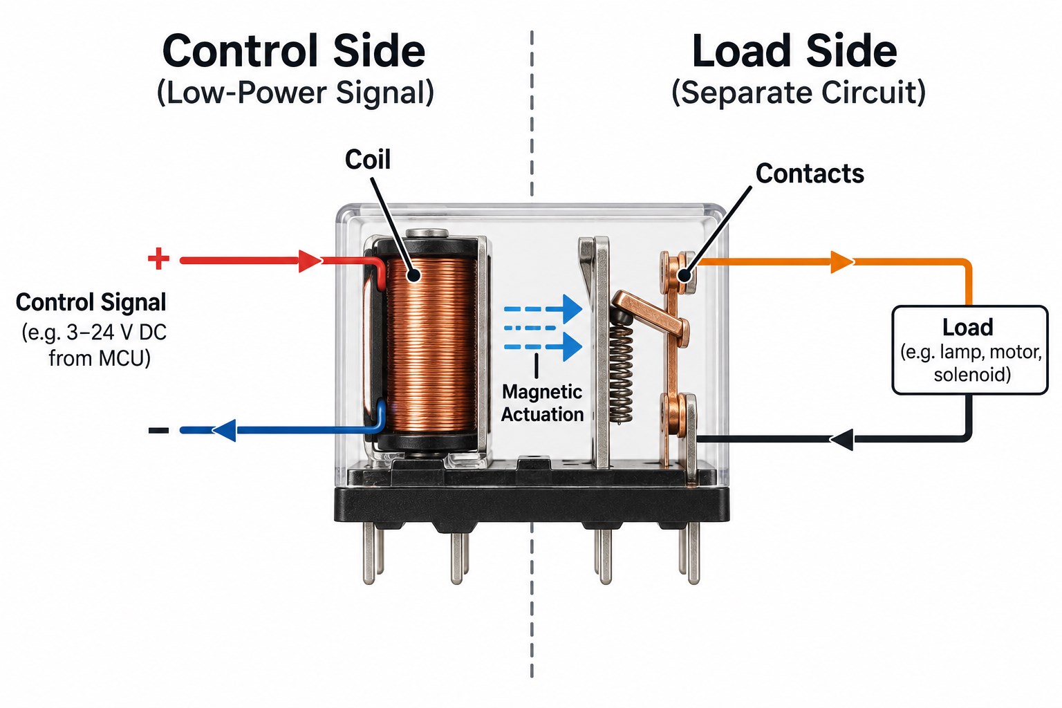
A button PCB works by converting a physical press into an electrical signal. When the user presses the button, the circuit changes state. The product may turn on, reset, select a mode, trigger a command, or send an input signal to a controller.

But from a PCB/PCBA manufacturing point of view, the button is not just a simple on/off point. It is a mechanical-electrical interface. That interface has to survive soldering, handling, enclosure assembly, repeated pressing, vibration, and possible contamination.

A button PCB normally needs attention to:

  • Copper pad shape and spacing
  • Solder mask opening
  • Surface finish
  • Switch footprint accuracy
  • Component height and orientation
  • Enclosure clearance
  • Cable or connector access near the button
  • Test point access
  • Rework possibility
  • Cleaning and contamination risk

For metal dome or contact pad style buttons, the surface condition is especially important. If the pad design, plating, or cleanliness is not controlled, the button may feel correct mechanically but fail electrically after repeated use.

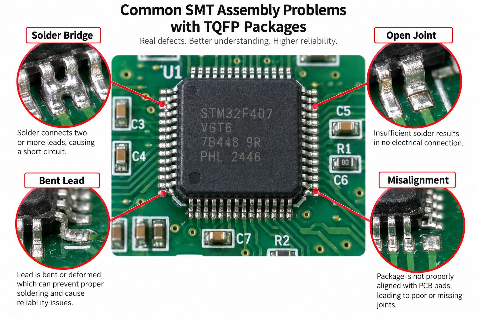
For SMT tactile switches, the biggest risks are usually solder bridging, insufficient solder, floating parts, shifted components, weak joints, or wrong orientation. For through-hole buttons, risks often include poor hole fit, insufficient solder fill, tilted assembly, or stress from the enclosure.

That is why button PCB projects should be reviewed as PCB + component + assembly + mechanical fit, not as a single isolated circuit symbol.

PCB button
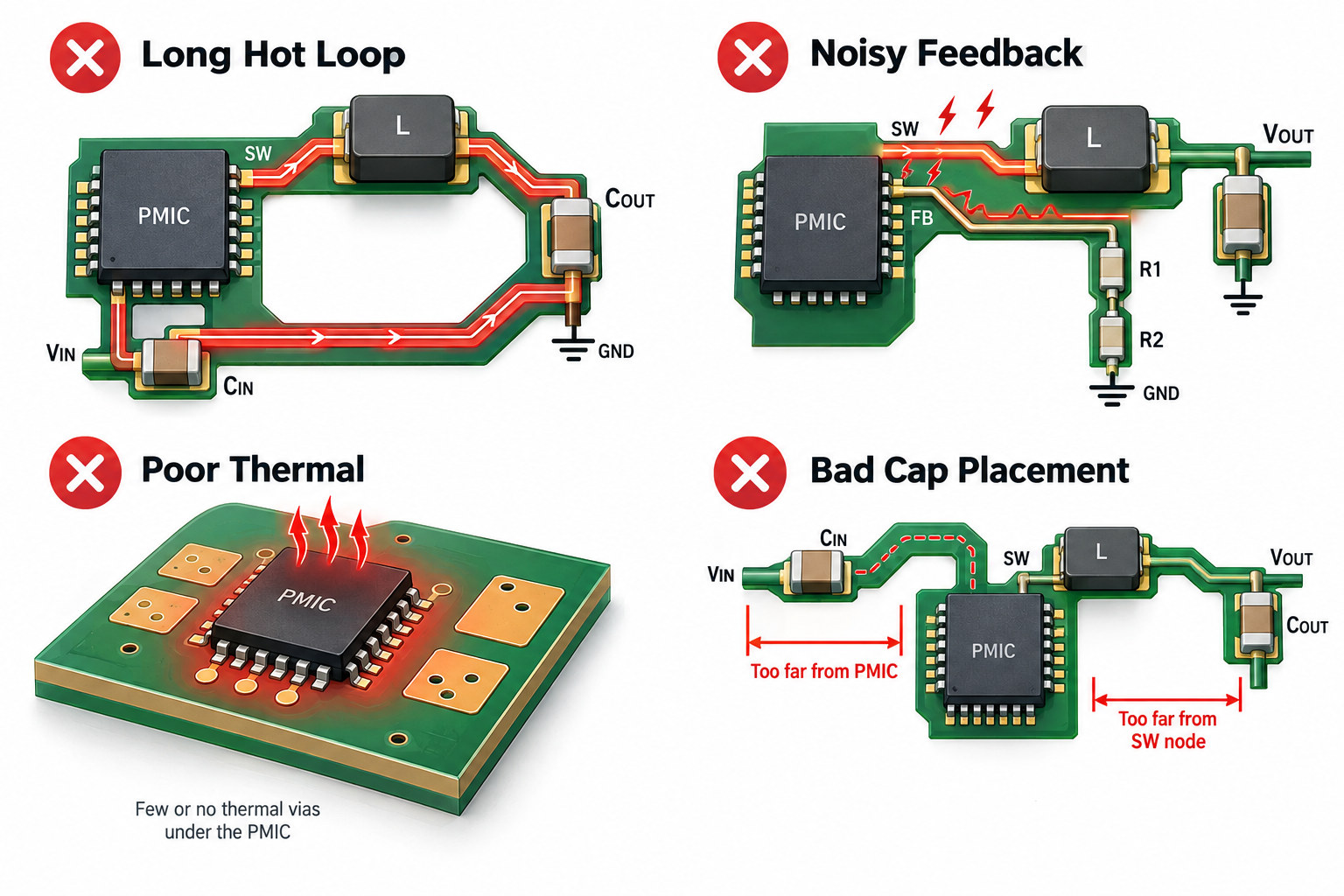
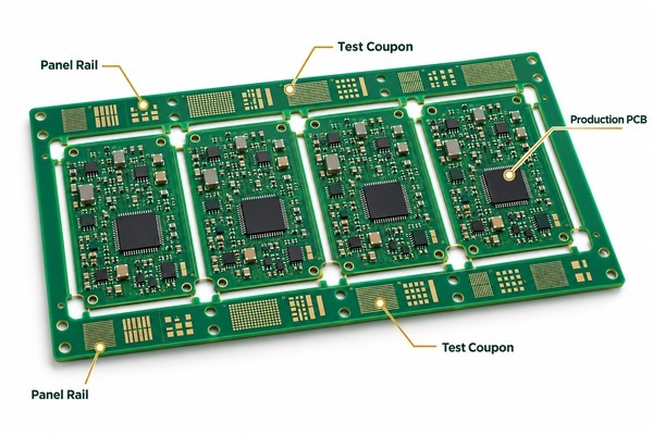
Button PCB inspection should confirm switch placement, solder joints, actuator direction, and access for testing or rework.

PCB Push Button Switch Options for SMT and Through-Hole Assembly

A PCB push button switch can be assembled in different ways depending on product structure, force requirement, board thickness, and production volume.

Common assembly options include:

  • SMT tactile switch: compact, common for small electronics, suitable for automated placement
  • Through-hole push button: stronger mechanical anchoring, useful when pressing force is higher
  • Right-angle switch: useful when the user presses from the side of the enclosure
  • Illuminated switch: used when the product needs both input and visual indication
  • Metal dome contact: thin structure, often used in keypads and control interfaces
  • Rubber keypad over PCB contacts: useful for sealed or multi-button interfaces

Each option changes the PCB and PCBA requirements.

SMT switches are efficient for automated assembly, but they need accurate stencil design, stable placement, and reflow compatibility. If the switch is too close to tall components, a shield, a housing wall, or a connector, it may be difficult to inspect or rework.

Through-hole assembly may provide stronger mechanical support, but it needs correct hole diameter, pad size, soldering method, and solder fill inspection. If the board is too thin or the switch is pressed heavily without enclosure support, the solder joints may carry too much mechanical stress.

Metal dome buttons can save height and provide a clean keypad feel, but the contact pad design, surface finish, adhesive layer, dome position, and cleanliness must be controlled carefully.

The best choice depends on the product, not only the switch price.

For a handheld tester, a low-profile SMT switch may be enough. For an industrial control panel, a through-hole or mechanically supported switch may be safer. For a sealed keypad, a metal dome or rubber keypad structure may fit better.

PCB Board Button Requirements Before Manufacturing

Before manufacturing a PCB board button project, the engineering files should make the button structure clear. If the drawing only says “button” without component details, the supplier may quote the PCB but miss assembly risks.

Project requirements should include:

  • Gerber files
  • BOM with manufacturer part number
  • Pick-and-place file for assembly
  • Assembly drawing
  • Switch footprint or land pattern
  • Button height requirement
  • Enclosure or mechanical drawing if available
  • Surface finish requirement
  • Test requirement
  • Expected order quantity
  • Prototype or mass production schedule

If the button is part of a customer-facing interface, the mechanical drawing becomes especially important. A button may pass electrical testing but still fail in the final enclosure if the actuator is too low, too high, off-center, or blocked by a housing rib.

Another important point is panelization. If the PCB includes edge buttons, side buttons, or buttons near a cutout, the panel design must not create stress during depaneling. Poor depaneling can crack solder joints, shift components, or damage nearby pads.

For buyers, the safest approach is to send both electrical and mechanical information before quotation. This helps the supplier check not only whether the board can be made, but whether the button can be assembled, inspected, tested, and used reliably.

Circuit Board Push Button Switch Assembly Risks to Check Early

A circuit board push button switch looks simple, but it can create production problems if reviewed too late. Many issues are not found in the schematic. They appear during SMT placement, soldering, enclosure assembly, or functional testing.

Key assembly risks include:

  • Wrong footprint: the switch pins do not match the PCB pads or holes.
  • Wrong orientation: the actuator direction does not match the enclosure.
  • Weak solder joint: the switch receives pressing force but has limited mechanical support.
  • Height mismatch: the button does not reach the enclosure keycap correctly.
  • Poor clearance: nearby parts block pressing, inspection, or rework.
  • Solder bridging: fine switch terminals receive too much solder paste.
  • Insufficient solder: the switch works at first but fails after repeated pressing.
  • Flux or contamination: contact areas become unstable.
  • Missing test access: the button function cannot be checked efficiently after assembly.

A real production issue often begins with one small assumption. For example, a customer may reuse a tactile switch footprint from an older project. The new switch looks similar, but the terminal spacing is slightly different. During assembly, the switch can still sit on the board, but solder wetting is uneven. The first samples may pass, while some production units later show intermittent button response.

This is exactly the type of issue that DFM and assembly review should catch before production.

EBest Circuit can help review button-related manufacturing risks from the PCB and PCBA side, including footprint consistency, soldering method, component orientation, layout manufacturability, inspection access, and test requirements.

PCB Button Reliability Checks Before Mass Production

PCB button reliability is not only about whether the button works once. It is about whether the button keeps working after repeated operation, transportation, enclosure assembly, and real product use.

For prototype orders, the main goal is usually to confirm function and mechanical fit. For small-batch or production orders, the focus should move toward repeatability.

Important review points include:

  • Does the button align with the enclosure opening?
  • Does the switch height match the mechanical design?
  • Is the switch protected from excessive pressing force?
  • Are the pads strong enough for repeated operation?
  • Is the surface finish suitable for the contact structure?
  • Can AOI or visual inspection see the solder joints?
  • Does the test fixture confirm button response?
  • Is rework possible without damaging nearby components?
  • Are the switch and PCB process compatible with lead-free reflow?
  • Does the assembly drawing clearly show polarity or orientation?
PCB button
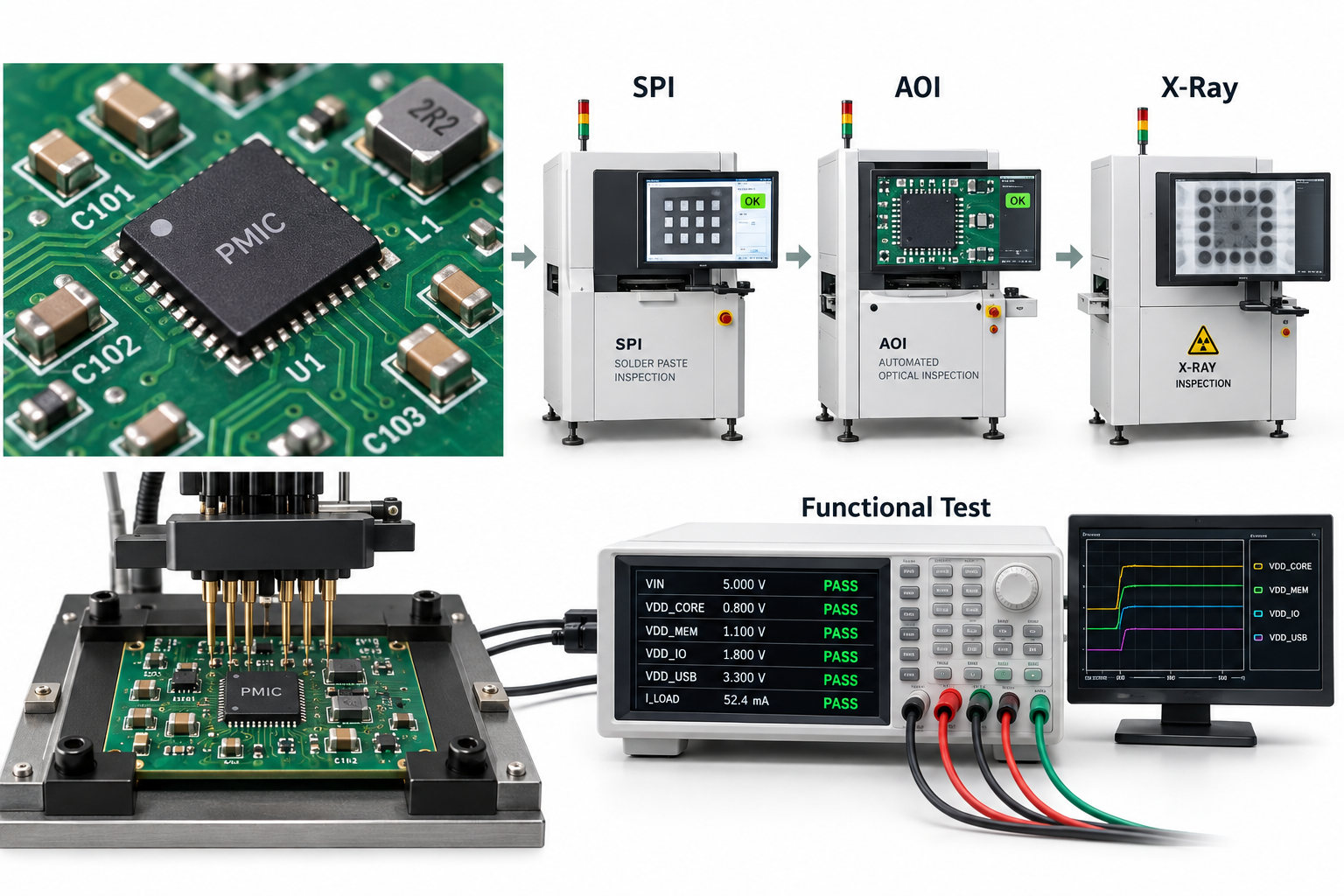
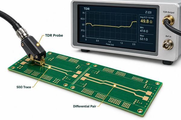
A good PCB button production review connects footprint, height, soldering, inspection, and functional testing before mass production.

For contact pad or metal dome style PCB buttons, surface finish and cleanliness deserve extra attention. ENIG, hard gold, carbon contacts, or other contact finishes may be considered depending on the product requirement, but the final selection should be confirmed based on use conditions and manufacturer capability.

For tactile switch assembly, the focus is usually solder joint quality, placement accuracy, reflow profile compatibility, and mechanical stress after enclosure installation.

A good production plan should define what is checked at incoming material, SMT/THT assembly, visual inspection, functional testing, and final packing. Without this plan, button failures may only appear after the product is assembled into the housing, when repair becomes much slower and more expensive.

How EBest Circuit Supports PCB Button PCB and PCBA Projects

EBest Circuit (Best Technology) supports PCB button projects by reviewing the manufacturing and assembly details that affect real production quality. The goal is not to replace the customer’s product design team, but to help make approved PCB files easier to manufacture, assemble, inspect, and test.

EBest Circuit supports PCB button projects with:

  • PCB fabrication for prototype, small-batch, and production orders
  • PCB layout manufacturability review
  • DFM review before production
  • BOM and component sourcing coordination
  • SMT assembly
  • Through-hole assembly
  • Mixed SMT and THT assembly
  • Inspection support such as AOI, visual inspection, and solder joint checks
  • Functional testing support according to customer requirements
  • One-stop PCB and PCBA service for engineering teams

For button PCB projects, EBest Circuit can help check whether the switch footprint matches the BOM, whether the assembly drawing is clear, whether the button position may create soldering or inspection risk, and whether the project should use SMT, through-hole, or mixed assembly.

This is useful for engineers who already have product design files but need a manufacturing partner to help turn those files into reliable boards and assembled PCBAs.

If the project includes uncertain component availability, EBest Circuit can also help review sourcing options and communicate with the customer before production. This reduces the risk of replacing a switch with a “similar” part that does not match the footprint, height, actuator direction, or production process.

For project review, send Gerber files, BOM, pick-and-place file, assembly drawing, and any enclosure or test requirement to sales@bestpcbs.com.

PCB Button Project Example for an Industrial Control Panel

A practical PCB button project may look simple at the RFQ stage, but the details decide whether production is smooth.

A customer developing an industrial control panel needed a small PCBA with several user-input buttons, indicator LEDs, and connectors. The first prototype used SMT tactile switches because the product needed a compact board size and automated assembly. The electrical function was simple, but the mechanical use condition was not: operators would press the buttons repeatedly while wearing gloves, and the board would be fixed behind a plastic front panel.

Project requirements:

  • Application: industrial control panel
  • Board type: FR4 PCB with SMT assembly
  • Key components: tactile switches, LEDs, connectors, resistors, controller-related components supplied by customer BOM
  • Order stage: prototype PCB assembly validation before small-batch production
  • Main concern: button alignment, solder joint strength, and functional testing
  • Delivery goal: fast prototype build for enclosure trial

During manufacturability review, several issues needed attention.

The first issue was switch height. The selected tactile switch was close to the required height, but the enclosure keycap tolerance was not clearly shown. If the switch sat slightly lower after soldering, the user might feel weak feedback. If it sat too high, the button might be partially pressed after enclosure assembly.

The second issue was component clearance. Two connectors were placed close to the button area. Electrically, the layout worked. Mechanically, the operator’s pressing direction and enclosure ribs could make inspection and rework difficult.

The third issue was soldering repeatability. The switch pads were small, and too much solder paste could cause uneven seating. Too little paste could create weak joints. The stencil opening and placement accuracy needed to be controlled for the prototype.

The fourth issue was testing. The customer originally planned only a visual check, but visual inspection could not confirm whether every button triggered correctly after assembly. A simple functional test was added to confirm button response before packing.

EBest Circuit solution:

  • Reviewed the switch footprint against the BOM
  • Checked button position and assembly direction
  • Confirmed SMT assembly process for the tactile switches
  • Flagged mechanical clearance points for customer confirmation
  • Supported PCBA assembly and functional testing based on customer files
  • Helped the customer prepare the prototype for enclosure validation

This kind of project shows why a PCB button should be reviewed as part of the full product build. The circuit may be simple, but the final success depends on PCB layout, component match, assembly control, enclosure fit, and test coverage.

FAQs About PCB Button

What is a PCB button?
A PCB button is a button function built on or mounted to a printed circuit board. It may use a tactile switch, metal dome, contact pad, rubber keypad, or push-button switch structure.

Is a PCB button the same as a PCB switch?
Not always. A PCB button usually describes the user input function, while a PCB switch describes the switching component or structure used to create that function.

Can EBest Circuit manufacture PCB button boards?
Yes. EBest Circuit can support PCB fabrication, DFM review, component sourcing coordination, PCBA assembly, inspection, and testing support for PCB button projects based on customer-approved files.

What files are needed for a PCB button PCBA quote?
Gerber files, BOM, pick-and-place file, assembly drawing, switch part number, button height requirement, surface finish requirement, and test requirement are recommended.

What causes PCB button failure after assembly?
Common causes include wrong footprint, poor solder joints, wrong switch orientation, enclosure interference, weak mechanical support, contamination, poor contact pad design, or missing functional testing.

In Conclusion, a PCB button may be small, but it connects electrical design, PCB fabrication, component sourcing, PCBA assembly, mechanical fit, and final user experience. To avoid production delays or unreliable button response, buyers should define the switch type, footprint, height, surface finish, assembly method, and test requirement before manufacturing.

EBest Circuit (Best Technology) supports PCB and PCBA projects that need reliable button assembly, DFM review, sourcing coordination, inspection, and testing support. If you need help reviewing a PCB button project before prototype or production, contact sales@bestpcbs.com.

You may also like

Transparent PCB Manufacturing Guide | Clear PCB Board

August 3rd, 2026

Transparent PCB is used when the circuit board itself needs to support visual inspection, light transmission, compact appearance, or optical product integration. It can appear in display modules, LED products, wearable electronics, sensors, medical devices, automotive lighting, transparent touch interfaces, and demonstration electronics.

For buyers and engineers, the real question is not only “Can the PCB be transparent?” It is also “Can the transparent PCB board be manufactured, assembled, inspected, and delivered without scratches, residue, soldering problems, or material mismatch?” EBest Circuit (Best Technology) supports custom PCB, FPC, special PCB, component sourcing, SMT assembly, inspection, and small-batch PCBA projects. If your project involves transparent PCB, transparent FPC, clear PCB board, or special optical electronics, please send your Gerber files, stackup, BOM, drawing, material notes, and assembly requirements to sales@bestpcbs.com for engineering review before production.

transparent PCB
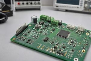
Transparent PCB materials and clear circuit structures need both visual and manufacturing review.
What Is a Transparent PCB?

A transparent PCB is a printed circuit board made with a clear or semi-transparent substrate instead of a normal opaque FR4 board. The purpose is to let light pass through the board or allow the internal circuit structure to remain visible.

A transparent PCB may be rigid or flexible, depending on the material and product structure. It may use transparent flexible film, transparent rigid substrate, transparent polyimide, PET, or selected glass-based circuit substrates for special optical electronics. The copper traces, pads, solder joints, and components are usually still visible, so the finished board is not “invisible.” It is more accurate to describe it as a clear or light-transmitting circuit board.

A transparent PCB project usually needs attention to:

  • Optical clarity
  • Material transmittance
  • Copper pattern visibility
  • Surface scratches
  • Solder mask choice
  • Adhesion reliability
  • SMT assembly compatibility
  • Residue after cleaning
  • Handling and packing protection

For simple display samples, appearance may be the main concern. For functional electronics, the board must also meet electrical, mechanical, thermal, and assembly requirements.

Transparent PCB Board Materials

Transparent PCB board performance depends heavily on material choice. Different materials have different transparency, flexibility, heat resistance, cost, process difficulty, and assembly limits.

Common material options include:

MaterialTypical Use
PETCost-sensitive transparent flexible circuits
Transparent PIHigher-temperature flexible circuits
Clear rigid substrateTransparent rigid PCB applications
Glass-based substrateOptical, display, sensor, or special transparent electronics
Transparent ceramic substrateSelected optical and thermal applications
Acrylic or PC-based materialsSelected display or structural electronics
transparent PCB
Material choices for transparent PCB projects should match transparency, flexibility, heat, and assembly requirements.

PET may be useful for low-cost transparent flexible circuits, but its heat resistance and SMT process window must be checked carefully. Transparent PI can offer better temperature performance than PET in some applications. Clear rigid substrates may be suitable when the project needs a board-like structure with visible circuitry.

Glass-based circuit substrates and transparent ceramic substrates are more specialized. They should not be treated like standard FR4 PCB materials. They may be considered for optical, display, sensor, LED, or special transparent electronics projects, but manufacturing feasibility depends on substrate type, metallization, drilling or interconnection method, assembly process, and inspection requirement.

For purchasing, the material name alone is not enough. The project should define transparency target, board thickness, copper thickness, temperature requirement, bending requirement, surface finish, assembly method, and visual acceptance standard.

Transparent Circuit Board vs Clear PCB Board

A transparent circuit board and a clear PCB board are often used to describe similar products, but the wording may reflect different customer expectations.

TermCommon Meaning
Transparent circuit boardFocuses on circuit visibility and light transmission
Clear PCB boardFocuses on clear substrate appearance
Transparent PCBGeneral search term for transparent printed circuit boards
PCB transparentSearch variation used by buyers or engineers
Clear PCBShorter phrase for transparent-looking PCB

In real manufacturing, the important point is not the name. The important point is the required function.

Before production, the supplier should confirm:

  • Is the board mainly for appearance or optical function?
  • Does the board need to transmit light evenly?
  • Will it be bent or kept rigid?
  • Does it need SMT assembly?
  • What surface finish is required?
  • Are scratches, haze, or residue unacceptable?
  • Will the product be used near heat, light, moisture, or vibration?

A board used in a transparent display module has different priorities from a board used in a wearable sensor, LED lighting product, or demonstration device.

Transparent Flex PCB and Transparent FPC

Transparent flex PCB, also called transparent FPC, is one of the most practical transparent circuit formats. It is usually used when the product needs both circuit connection and flexibility.

Transparent FPC may be used in wearable electronics, transparent touch modules, display connections, medical sensors, LED light strips, flexible user interfaces, automotive lighting, and compact optical modules.

The key advantage is flexibility. The challenge is that transparent flexible materials can be more sensitive to heat, handling, scratches, bending radius, adhesive choice, and surface contamination.

For transparent FPC review, useful checks include:

  • Film thickness
  • Copper thickness
  • Bend area
  • Stiffener requirement
  • Connector area reinforcement
  • Coverlay or insulation opening
  • Surface finish
  • SMT temperature compatibility
  • Final packing method

If the transparent FPC needs components assembled on it, the SMT process must be reviewed carefully. Reflow temperature, solder paste, component weight, panel design, and fixture support can affect yield. For projects that require assembly on flexible circuits, flex PCB assembly review is especially useful before production.

Transparent Rigid PCB Manufacturing Checks

Transparent rigid PCB projects are different from standard FR4 boards. The board may need a transparent rigid substrate, special solder mask, controlled appearance, and careful handling through fabrication and assembly.

Important manufacturing checks include:

  • Substrate transparency
  • Board thickness tolerance
  • Copper adhesion
  • Trace and spacing capability
  • Via drilling and plating
  • Surface finish compatibility
  • Solder mask transparency or opening design
  • Silkscreen visibility
  • Warpage control
  • Edge quality
  • Scratch prevention

For normal FR4 boards, a minor cosmetic mark may not matter much. For a transparent PCB board, visual defects are easier to notice. Scratches, fingerprints, haze, flux residue, and uneven solder mask can become customer-facing quality issues.

That means the inspection plan should include both electrical performance and appearance requirements.

PET, Transparent PI, and Glass-Based Circuit Substrates

PET, transparent PI, clear rigid substrate, and glass-based circuit substrates are not interchangeable. They serve different product needs.

Material choice should follow the real application:

  • Use PET when cost, flexibility, and light transparency are the main priorities.
  • Use transparent PI when better heat resistance or flexible circuit reliability is needed.
  • Use clear rigid substrate when the product needs a board-like structure with visible circuitry.
  • Consider glass-based circuit substrates only when optical stability, flatness, display integration, or special transparent electronics requirements justify a different manufacturing route.
  • Consider transparent ceramic substrate only when the project has both optical and thermal requirements and the manufacturing process is confirmed.

The biggest mistake is choosing a material only because it looks clear. A transparent PCB still needs to survive fabrication, assembly, testing, shipping, and real product use.

For example, if the product needs SMT assembly, the material must tolerate the soldering process. If the product needs bending, a glass-based substrate is not suitable. If the product must manage heat, PET may not be enough. If the board is part of an optical product, haze, reflection, scratches, and surface cleanliness may matter as much as electrical performance.

SMT Assembly for Transparent PCB Projects

SMT assembly for transparent PCB projects needs more care than many standard boards because appearance and function are both visible.

transparent PCB
Transparent PCB assembly needs careful handling, cleaning, inspection, and packing to protect visible circuit areas.

Assembly risks include:

  • Flux residue on clear areas
  • Solder balls near optical zones
  • Scratches during handling
  • Component skew
  • Poor wetting on special pads
  • Material deformation during reflow
  • Connector stress
  • Cleaning marks
  • Packing damage

For transparent FPC or thin transparent boards, panel support is especially important. The board may need a carrier, fixture, stiffener, or custom panel design to keep it stable during printing, placement, reflow, and inspection.

EBest Circuit can review:

  • BOM and component availability
  • SMT temperature compatibility
  • Panelization
  • Fiducial marks
  • Stencil and solder paste requirements
  • Connector assembly method
  • Cleaning requirement
  • Visual inspection standard
  • Individual packing needs

The goal is to keep the approved transparent area clean and protect the board from avoidable assembly damage.

Transparent PCB Applications in Electronics

Transparent PCB applications are usually found where appearance, light transmission, compact structure, or optical integration matters.

Common applications include transparent display modules, LED lighting products, wearable electronics, medical sensor devices, smart glass modules, automotive lighting and indicators, consumer electronics prototypes, touch panels, optical sensors, and educational or demonstration electronics.

For buyers, the application should guide the manufacturing decision. A transparent LED product may care about light uniformity and heat. A wearable product may care about bending and skin-contact reliability. A sensor module may care about cleanliness and optical interference. A display-related project may care about haze, scratches, alignment, and visual appearance.

This is why transparent PCB manufacturing should not be quoted only by board size and layer count. The supplier should understand how the board will be used.

Transparent PCB Manufacturing Case Study

A European customer needed a small-batch transparent FPC prototype for a smart display module. The product required a visible circuit area, a flexible connection section, and SMT assembly for several small components.

Project requirements:

  • Customer region: Europe
  • Application: Smart display module
  • PCB type: Transparent flexible circuit
  • Quantity: Prototype and small-batch validation
  • Key concern: Appearance, flexibility, soldering reliability, and clean delivery
  • Assembly need: SMT components and connector area reinforcement
  • Packing need: Individual protection to avoid scratches

Main challenges:

  • The clear circuit area had to remain clean after SMT.
  • The flexible section needed stable bending performance.
  • The connector area required reinforcement.
  • The customer needed samples for appearance and function review.

  • Flux residue and handling marks could affect customer approval.

EBest Circuit review process:

  • Checked the Gerber, outline, connector area, and flexible section.
  • Reviewed the material and thickness against the bending requirement.
  • Confirmed the SMT process window before assembly.
  • Planned panel support to reduce deformation during placement.
  • Paid attention to cleaning, visual inspection, and packing.
  • Protected finished boards individually before shipment.

Result:

The customer received transparent FPC samples suitable for display-module validation. The value was not only making a clear circuit board. The value was keeping the material, SMT process, connector area, appearance requirement, and packing method connected from file review to delivery.

For transparent PCB projects, this kind of early review matters because many problems are difficult to fix after assembly.

FAQs About Transparent PCB

  1. What is a transparent PCB?
    A transparent PCB is a printed circuit board made with a clear or light-transmitting substrate. It may be rigid or flexible, depending on the material and product use.
  2. What is the difference between transparent PCB and transparent FPC?
    Transparent PCB is the general term. Transparent FPC usually refers to a flexible transparent circuit made with transparent film materials such as PET or transparent PI.
  3. Can transparent PCB support SMT assembly?
    Some transparent PCB and transparent FPC projects can support SMT assembly, but the material, reflow temperature, panel support, surface finish, and cleaning requirement must be reviewed before production.
  4. Is transparent PCB the same as glass PCB?
    No. Glass-based circuit substrates are one possible option for special optical or transparent electronics, but they are different from standard FR4 PCB and transparent FPC manufacturing.
  5. What should I send for a transparent PCB quotation?
    Send Gerber files, stackup or material requirement, board thickness, copper thickness, transparency requirement, BOM, assembly files, drawing, quantity, and any appearance or packing notes.

All in all, a transparent PCB project needs more than a clear substrate. It needs the right material, controlled manufacturing, clean assembly, careful inspection, and protective packing. If your project involves transparent PCB board, transparent FPC, clear PCB board, or optical electronics PCBA, please send your files and requirements to sales@bestpcbs.com. EBest Circuit can help review the manufacturing path before your project moves into production.

You may also like

What Is a Solder Fillet? Good Shapes, Common Defects and IPC Criteria

August 3rd, 2026

A solder fillet is the visible solder profile that joins a component termination to a PCB land. Its shape provides evidence of wetting, solder volume, alignment and process balance, but appearance alone cannot establish the electrical integrity or long-term reliability of every joint. Accurate evaluation depends on the termination type, package construction, product class, customer requirements and applicable acceptance criteria.

A sound evaluation starts with fillet formation and visible heel, toe and side profiles, then accounts for SMT, through-hole and package-specific differences. Pad design, solder volume, wetting and reflow explain many defects; inspection criteria, prevention and corrective action determine what happens next.

Solder fillet examples on an unbranded populated PCB

What Is a Solder Fillet and How Does It Form?

A solder fillet forms through wetting and solidification. Molten solder wets the PCB land and component termination, then solidifies into a continuous metallurgical connection. The visible curve is only the outside portion of the joint. Its final profile depends on solder volume, surface condition, geometry, gravity, surface tension, component standoff and the heating and cooling cycle.

SMT fillets form during solder-paste reflow. Solder paste is printed onto the lands, components are placed, and the assembly moves through reflow. The flux activates as temperature rises, helping remove light oxides. Solder particles melt, spread over solderable surfaces and pull the termination toward equilibrium. During cooling, the alloy solidifies and preserves the resulting fillet geometry.

Through-hole fillets form around a lead and plated barrel. Solder enters from the solder-source side during wave, selective or hand soldering. Wetting and capillary action help solder rise through the barrel and connect the lead, hole wall and land. The visible soldering fillet on either side must therefore be considered with barrel fill, circumferential wetting and lead condition.

Fillet formation follows a controlled sequence:

  1. Confirm that the land, finish and component termination are solderable and free of harmful contamination.
  2. Deposit or deliver the solder volume required by the footprint and termination.
  3. Align and support the component so its termination overlaps the intended land.
  4. Apply a thermal cycle that activates the flux and heats both joining surfaces sufficiently.
  5. Allow molten solder to wet and spread without movement, excessive oxidation or premature cooling.
  6. Cool the joint under controlled conditions, then inspect it against the correct criteria.

What Do Good Heel, Toe and Side Soldering Fillet Shapes Look Like?

Good fillets show continuous wetting and controlled solder volume. Heel, toe and side evidence must suit the lead and land geometry without hiding the joint or bridging adjacent conductors. A smooth concave transition is useful on many visible SMT joints, but it is not a universal acceptance template.

  • Heel fillet: Look for a continuous transition at the inside bend or rear of a gull-wing lead. Gaps, cracks, lifted leads or a visibly starved joint require closer evaluation.
  • Toe fillet: Where the termination design permits visible toe wetting, check the lead end and land for continuous coverage without bridges, solder balls or an excessive mound.
  • Side fillet: Check both sides for consistent wetting, open edges, dewetting or asymmetry. QFN sidewalls may not wet unless the package has wettable flanks.

Fillet visibility depends on the termination geometry. A toe or side fillet is not equally visible or required for every termination, so package-specific criteria take precedence over a generic shape.

Do not judge a joint only by shine. Lead-free alloys can have a matte surface and still be acceptable, while a glossy joint can conceal incomplete wetting or excessive solder. Inspect the lead, land and solder as one connection. Compare both ends of two-terminal components because unequal fillet volume can indicate paste imbalance, component offset or uneven heating.

Excess solder at an MLCC termination can increase stress during board bending. The largest fillet is not automatically the best. The joint still needs sufficient wetting and solder volume within the component manufacturer’s land-pattern and mounting guidance.

Why Does Solder Fillet Geometry Affect Solder Joint Reliability?

Fillet geometry changes electrical and mechanical load transfer. Too little connected area can reduce mechanical margin or create an intermittent open. Excess solder can obscure evidence, bridge conductors, increase stress on fragile terminations or produce a shape that is difficult to inspect consistently.

A solder joint expands and contracts as the component and PCB cycle through temperature changes. Differences among the package, copper, laminate and solder concentrate strain in the interconnect. Joint height, cross-sectional area, lead compliance, alloy, pad size and package stiffness all affect that strain. Geometry contributes to reliability, but it cannot predict service life by itself.

A controlled CALCE study examined reworked surface-mount assemblies. Uneven and reduced joint heights affected temperature-cycling performance for the tested leadless resistor configuration, but the tested gull-wing package did not show the same response. The result is package- and test-specific; it does not establish a universal fillet-height limit.

Geometry must be evaluated against the assembly’s actual thermal, vibration and current loads. Visual acceptance does not prove service life. Products exposed to severe loads need application-appropriate electrical, mechanical or environmental validation in addition to fillet inspection.

How Do SMT and Through-Hole Solder Fillets Differ?

SMT and through-hole fillets form through different processes. SMT fillets form on surface lands through paste printing and reflow. Through-hole fillets form around leads and plated barrels during wave, selective or hand soldering. Their visible evidence and inspection requirements are not interchangeable.

Comparison Dimension SMT Solder Fillet Through-Hole Solder Fillet
Connection geometry Termination overlaps a surface land Lead passes through a plated barrel
Primary solder source Printed solder paste Wave, selective nozzle or solder wire
Key design inputs Land pattern, stencil aperture, mask and component standoff Hole-to-lead relationship, annular land, barrel plating and lead protrusion
Visible evidence Heel, toe and side wetting where accessible Fillet, circumferential wetting and lead condition
Common defect drivers Paste release, placement, coplanarity and reflow imbalance Fluxing, preheat, wave contact, hole design and thermal demand
Typical inspection Visual, AOI, 3D optical measurement and X-ray for hidden joints Visual inspection plus barrel-fill or sectional evidence when required

A through-hole joint is not acceptable merely because it forms a rounded mound. A large convex profile can hide poor wetting or incomplete barrel fill. An SMT chip joint should not be rejected simply because it lacks the cone-like shape of a through-hole joint. Use termination-specific acceptance criteria.

How Should QFN, Gull-Wing, J-Lead and Castellated Solder Fillets Be Evaluated?

Evaluate packages by visible surfaces and hidden-joint risk. Gull-wing leads offer relatively clear heel, toe and side views. J-leads hide part of the connection beneath the inward-curved lead. QFNs place most of the joint under the package, while castellated modules expose edge terminations for side-fillet inspection.

Package or Termination Visible Fillet Evidence Hidden or Ambiguous Area Primary Design/Process Concern Verification Approach
Gull-wing lead Heel, toe and both sides are often accessible Interface directly beneath the lead Lead coplanarity, paste volume and fine-pitch bridging Controlled visual inspection or AOI with escalation for uncertain joints
J-lead Outer side and portions of the lead-to-land transition Connection under the curved lead Placement, land length and limited viewing access Multiple viewing angles; additional method if acceptance remains uncertain
QFN Side fillet only where the termination design supports wetting Bottom perimeter lands and exposed thermal pad Stencil segmentation, paste balance, voiding, standoff and sidewall finish AOI for visible flanks plus X-ray or other evidence for hidden connections
Castellated module Side wetting along the plated half-hole and host-board land Interface beneath the module edge Castellation plating, land extension, coplanarity and paste release Side-view optical inspection with electrical verification as required

QFN inspection requires package-specific evidence. Some packages use wettable flanks specifically to promote visible side wetting and improve AOI discrimination. Other QFN sidewalls are not intended to wet in the same way. Limited side solder therefore does not automatically prove that the hidden bottom joint is defective. Check the component datasheet and package drawing before creating a local reject rule.

For a new footprint, compare the land pattern with the component manufacturer’s current recommendation. Confirm the exposed-pad design, paste segmentation, mask clearances and via treatment. A generic QFN footprint can create excess center-pad solder, package float or perimeter opens even when the reflow oven is functioning correctly.

How Do Pad Design, Solder Volume and Reflow Affect Solder Fillet Geometry?

Pad geometry, solder volume and reflow act as one system. The pad defines where solder can spread, the stencil controls the deposited volume, and reflow determines whether the deposit wets and solidifies evenly. Oven settings cannot correct an unsuitable land pattern or blocked aperture.

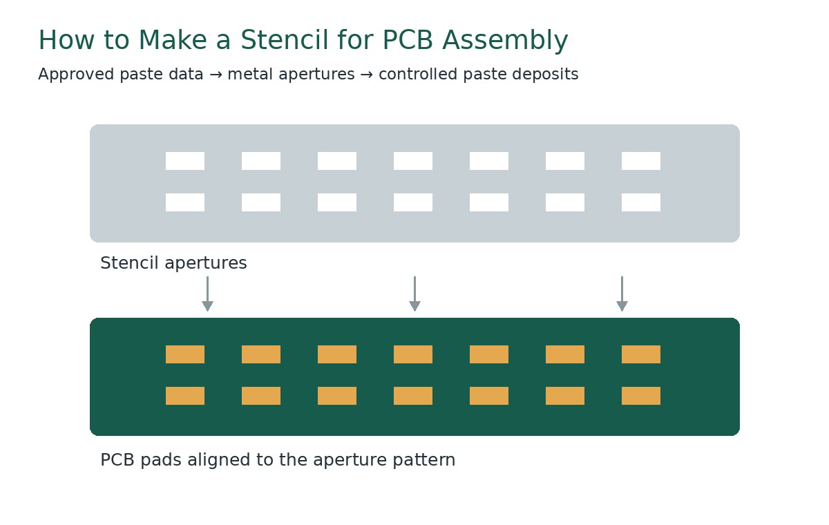
PCB and stencil review for pad design and solder volume control

Use the following sequence during design and process setup:

  1. Start with the package drawing. Verify termination dimensions, tolerances, standoff and the manufacturer’s recommended land pattern.
  2. Define the PCB lands. Provide the overlap and inspection access required by the component without creating unnecessary exposed copper or bridge risk.
  3. Coordinate solder mask. Check mask registration, dams and whether solder-mask-defined or non-solder-mask-defined geometry is appropriate for that feature.
  4. Design stencil apertures. Set deposit area and volume by package, pitch and thermal demand. Segment large thermal-pad apertures where appropriate instead of printing one uncontrolled mass.
  5. Verify paste release. Review aperture wall quality, stencil cleanliness, board support, squeegee conditions and paste condition.
  6. Control placement. Confirm centering, rotation, lead coplanarity and placement force so the part does not squeeze paste away or sit outside the wettable area.
  7. Develop a board-specific profile. Measure the loaded assembly rather than copying a profile from a different board. Respect solder-paste and component thermal limits.
  8. Correlate results. Compare SPI, placement, reflow and post-reflow inspection by reference designator before changing limits.

Thermal balance matters at both ends of a chip component. A pad connected to a large copper area may heat differently from a pad connected to a narrow trace. Unequal melting and wetting forces can create uneven fillets or tombstoning. Review thermal relief, copper balance, aperture design and the reflow profile as one system.

What Causes Insufficient, Missing, Excessive or Uneven Solder Fillets?

Fillet defects usually start in delivery, wetting, placement or heat. Joint disturbance can add another failure path. Diagnose the visible symptom by confirming its location, repetition pattern and upstream process changes.

Observed Fillet Condition Likely Cause Categories Evidence to Check Risk or Limitation Corrective Direction
Insufficient solder fillet Low paste volume, poor release, undersized aperture, component/land mismatch SPI volume, stencil opening, paste transfer and joint location pattern Reduced connection area or intermittent/open behavior Restore controlled deposit and confirm footprint compatibility
Missing fillet Blocked aperture, severe nonwetting, missing paste or lifted termination Pre-placement paste image, AOI image, lead coplanarity and surface condition A hidden joint may still exist on some packages; visibility alone is inconclusive Separate deposition failure from package-visibility limitation
Excessive solder fillet Oversized aperture, thick stencil, duplicate solder addition or poor drainage Deposit volume, rework history, bridge clearance and component seating Can hide wetting, bridge conductors or stress fragile terminations Reduce or redistribute volume without starving the joint
Uneven fillets Paste imbalance, placement offset, unequal thermal mass or pad asymmetry Paired-pad SPI data, centroid, copper connections and profile traces May indicate unequal load transfer or impending tombstoning Balance design, printing, placement and heating

Defect patterns help isolate the failing process stage. If the same lead or reference designator is affected on multiple boards, first check the footprint, aperture and local copper. If missing or insufficient deposits occur randomly, examine stencil cleaning, paste roll condition, board support and printer stability. If acceptable SPI is followed by a poor joint, move the investigation to placement, solderability and reflow.

How Do Poor Wetting and Dewetting Affect Solder Fillet Shape?

Nonwetting leaves the basis metal exposed. Molten solder contacted the surface but did not form the required bond. Dewetting occurs after solder initially covers the surface and then recedes, leaving irregular solder mounds separated by thin solder-covered areas.

Wetting barriers are not solved by heat alone. Common causes include oxides, contamination, degraded finishes, insufficient flux activity and inadequate heat at the actual joint. Excessive time or temperature can also damage flux performance or promote surface reactions that worsen the result. Inspect storage history, finish condition, paste handling and measured thermal response before changing the profile.

Contact angle is evidence, not a universal limit. A large angle can warn that solder has not spread effectively, but three-dimensional geometry, viewing direction and component construction affect the measurement. Use it alongside continuous wetting, solder coverage, land/lead geometry and the applicable acceptance document.

Do not repeatedly reflow a poorly wetted joint. Extra heating can damage the pad, laminate or component and may create intermetallic growth without restoring a clean solderable interface. Quarantine the affected material, compare known-good samples, verify surface condition and approve any rework through a controlled instruction.

How Are Solder Fillets Inspected Against IPC Acceptance Criteria?

Inspect each fillet against termination-specific criteria. Apply the required product class, customer requirements and a method capable of seeing the relevant feature. IPC J-STD-001J defines soldered-assembly process and material requirements, while IPC-A-610J defines post-assembly acceptability criteria.

Microscope inspection of solder fillets against IPC acceptance criteria

Do not apply IPC criteria from an unrelated package. Before inspection, identify the assembly revision, product class, termination type and any customer-approved deviations. Use the current purchased standard and contract documents for the actual acceptance limits.

Inspection Method What It Evaluates Best-Fit Fillets or Packages Limitation Escalation Trigger
Controlled visual inspection Accessible wetting, cracks, bridges, solder quantity and lead position Through-hole, gull-wing, castellated and accessible chip joints Cannot prove hidden structure or electrical continuity Obscured interface, borderline condition or repeat defect
2D/3D AOI Visible geometry, component placement and programmed anomalies Production SMT with repeatable visible features Program limits and lighting can create false calls or escapes Hidden joint, uncertain side wetting or changing false-call rate
X-ray inspection Hidden solder distribution, opens, bridges and selected void evidence QFN, BGA, LGA and other bottom-terminated packages A 2D projection may overlap structures and does not show every interface condition Ambiguous image, critical defect or root-cause investigation
3D optical measurement Height, profile, area and repeatable visible geometry Accessible fillets requiring quantitative comparison Cannot see beneath an opaque package Correlation with destructive analysis is needed
Cross-section Internal interface, joint thickness, wetting and defect morphology Failure analysis and process validation samples Destructive and limited to the sampled location Unresolved systemic defect or qualification need

Inspection records must support traceable disposition. Identify the board, lot, reference designator, method, viewing conditions, applicable criterion and disposition. Store representative images when they support the decision, and correlate them with SPI and process records where possible. The solder joint inspection guide explains how to select visual, AOI, X-ray and destructive methods by defect visibility.

How Can Solder Fillet Defects Be Prevented During PCB Assembly?

Prevent defects by controlling the complete assembly chain. Control the footprint, material condition, solder deposition, placement and reflow, then use inspection feedback to identify recurring variation.

Use this production sequence:

  1. Review the design. Check component drawings, land patterns, copper balance, mask clearances, thermal pads, vias and through-hole geometry before releasing fabrication data.
  2. Confirm incoming condition. Protect PCB finishes and component terminations from contamination, moisture and uncontrolled storage exposure.
  3. Control and measure solder delivery. Verify stencil thickness, aperture design, paste condition, printer setup, board support and cleaning frequency. Use SPI where appropriate to detect missing, low, excessive or offset deposits before placement. The solder paste stencil guide covers recurring printing defects.
  4. Control component placement. Verify package orientation, centroid data, nozzle selection, placement force and lead coplanarity.
  5. Develop the thermal process. Profile the populated assembly, including thermally demanding locations, and work within material and component limits.
  6. Inspect and correlate results. Program AOI by package and product revision, use X-ray or another suitable method for hidden joints, and correlate SPI, placement, reflow and inspection results by board and reference designator.
  7. Control rework. Use approved materials, tools, temperature limits and verification steps. Repeated heating without root-cause removal can create new damage.
  8. Close the corrective-action loop. Confirm that the change removes the defect without causing bridging, component stress, voiding or another unintended condition.

Prevention must remain package-specific. Increasing paste may repair an insufficient gull-wing fillet but cause float or voiding under a QFN thermal pad. Raising peak temperature may improve one cold location but exceed a sensitive component’s limit elsewhere. Change one justified variable, verify the result across the board and retain the evidence needed for repeat production.

How Should an Insufficient Solder Fillet Problem Be Corrected in SMT Production?

Find where solder volume is lost before changing the process. Determine whether a recurring insufficient fillet begins during printing, placement, wetting or reflow, then use the following sequence to verify the correction.

  1. Contain the suspect lot. Identify affected boards and reference designators, then prevent uncertain assemblies from advancing without disposition.
  2. Confirm the defect definition. Compare the joint with the correct termination criteria and known-good samples. Exclude a package-visibility issue before calling the fillet missing.
  3. Map the pattern. Determine whether the condition repeats on the same pad, one board region, one stencil cycle or random locations.
  4. Review pre-reflow evidence. Check paste presence, area, height, volume and offset where SPI or retained images are available.
  5. Inspect the stencil and support. Look for aperture blockage, damaged walls, contamination, board flex or poor gasketing at the affected land.
  6. Verify component placement. Confirm centering, rotation, coplanarity and placement force. A lead outside the paste deposit can resemble a printing problem after reflow.
  7. Check solderability and heat. Compare finish condition, flux performance and measured profile at the affected location.
  8. Apply the smallest justified change. Clean or repair the stencil, correct support or alignment, adjust the aperture through engineering control, or revise the board-specific profile according to the confirmed cause.
  9. Run a controlled confirmation lot. Verify deposit and post-reflow fillet evidence at the target location while checking neighboring joints for excess solder, bridging or component movement.
  10. Update controlled records. Revise the stencil, program, work instruction or inspection limits only after the corrective result is repeatable and approved.

Adding solder does not prevent recurrence. Close the corrective action only after the confirmed cause, controlled change, verification result and repeat-build instruction agree.

FAQs About Solder Fillet

Q1: Can a solder fillet be accepted from a smartphone photo?
A1: Not as the sole acceptance record. An uncontrolled photo may hide scale, viewing angle, lighting and depth. Use controlled magnification, the correct termination criterion and the board’s traceable inspection record.

Q2: Can flux residue be mistaken for a solder fillet defect?
A2: Residue can obscure edges, contamination or fine bridging. Inspect under suitable lighting and magnification. Clean only when the assembly process and materials permit it, then reinspect the same location.

Q3: Should a board with a suspect fillet be electrically tested before disposition?
A3: Contain and assess the risk first. If the condition may create a short, lifted conductor or unstable connection, follow the approved inspection and disposition process before applying power.

Q4: What solder-joint requirements should a purchase order specify?
A4: Specify the governing acceptance requirements. State the standard revision, product class, customer-specific criteria, approved deviations, inspection records and required tests.

Q5: Should solder fillets be inspected before conformal coating?
A5: Inspect before coating obscures the joints. Retain images or machine records for locations that will be difficult to verify after coating.

Q6: How many times can a defective solder fillet be reworked?
A6: There is no universal rework count. The limit depends on the PCB, finish, component and approved repair instruction. Repeated heating can damage pads, laminate, coatings or the component.

Q7: How should AOI limits be established for a new package?
A7: Start with package data, criteria and controlled samples. Validate lighting and viewing angles with known acceptable and defective conditions, then place threshold changes under revision control.

Q8: When should PCB or component solderability be tested?
A8: Test after repeated, unresolved wetting failures. Separate PCB-finish evaluation from component-termination evaluation and use an agreed method.

Q9: Does a cleanliness test prove that a solder fillet is acceptable?
A9: No; cleanliness and joint acceptability are different attributes. Cleanliness testing evaluates residues under its test method, while fillet acceptance still requires termination-specific inspection and any required electrical evidence.

For an engineering review and quotation, send your Gerber or ODB++ files, BOM and placement data to EBest Circuit at sales@bestpcbs.com. Include the quantity, package requirements and acceptance criteria.

You may also like

High-Power Prototype Board for Passive Rectifier Design and Testing

July 31st, 2026

A high-power prototype board for a passive rectifier must carry capacitor-charging pulses without excessive voltage drop or overheating. It must also maintain the required insulation distances and provide guarded measurement access. Size the board from quantified input, load, surge, fault-energy, thermal, and test-duration limits.

In a capacitor-input rectifier, the diodes conduct near the AC waveform peaks rather than throughout each half-cycle. These narrow pulses raise RMS current, connector and copper loss, diode heating, inrush stress, and loop-induced overshoot above what an average DC-load calculation predicts.

high-power prototype board for a passive rectifier with capacitors, copper busbars, fuse, and heat sink on a white background

What Is a High-Power Prototype Board for a Passive Rectifier?

The board integrates the complete rectifier power path. It may carry a bridge or discrete diodes, a reservoir capacitor bank, fuses, inrush limiting, transient suppression, discharge resistors, current shunts, terminals, heat sinks, and guarded test points. Tests must establish output voltage and ripple, repetitive and surge-current capability, component temperatures, insulation integrity, and repeatable assembly.

What Input, Output, and Load Requirements Must Be Set Before Design?

Set worst-case electrical, thermal, and fault limits first. Nominal voltage and average output current do not cover input tolerance, waveform frequency, output ripple, startup charging, overload duration, cooling, enclosure conditions, or available short-circuit energy.

  • AC input: Record minimum, nominal, and maximum RMS voltage; frequency; number of phases; source impedance; isolation method; and expected transient category.
  • DC output: Define no-load and full-load voltage, allowable ripple, polarity, stored-energy limit, and whether the load tolerates an unregulated output.
  • Load profile: Separate continuous current, repetitive peak current, short-duration overload, regenerative behavior, and load steps.
  • Startup condition: State whether the capacitor bank may be discharged at turn-on and how often the unit can restart.
  • Environment: Specify maximum ambient temperature, airflow, altitude, pollution degree, humidity, enclosure orientation, and nearby heat sources.
  • Acceptance limits: Set maximum diode case temperature, capacitor surface temperature, busbar or terminal rise, output sag, ripple, and permitted test duration.

For a large transformer, mains-derived source, generator, or high-current secondary, define source isolation, available fault current, stored energy, discharge time, guarding, and the conditions that require protective earth.

For a sinusoidal single-phase source, bridge, and reservoir capacitor, the approximate no-load DC bus is the AC peak minus two conducting-diode drops: VDC ≈ √2 × VAC,RMS − 2VF. This estimate assumes the capacitor charges close to the waveform peak. Under load, transformer regulation, wiring resistance, diode conduction angle, capacitor ESR, and source impedance reduce the result. Use minimum input to check output compliance and maximum input to check voltage stress.

The load definition should also identify the actual current return. If a downstream converter draws narrow pulses, its local input capacitor and the rectifier capacitor interact through the wiring inductance. Testing only with a steady resistor may hide instability or peak-current stress that appears with the final electronic load.

How Do Passive Rectifier Topologies Affect High-Power Prototype Board Design?

Topology determines conduction loss, ripple, and loop geometry. Diode count and transformer use change the voltage and current stress on the source, semiconductors, copper, capacitors, and thermal system.

Topology Conducting Path Transformer Requirement Output Character Board Impact
Half-wave One diode per pulse Single winding Line-frequency ripple and poor source utilization Simple layout, but larger filtering and asymmetric source current
Center-tapped full-wave One diode and half the secondary per pulse Center-tapped secondary with matched half-windings Twice-line-frequency ripple Lower diode-path drop, higher diode reverse-voltage demand, three winding connections
Single-phase bridge Two diodes per pulse Single secondary winding Twice-line-frequency ripple Compact general-purpose solution; two forward drops and concentrated bridge heating
Three-phase six-pulse bridge Two diodes conduct at a time Three-phase source Six charging pulses per AC cycle and a shorter capacitor-discharge interval Six diode branches, three phase terminals, phase-to-phase spacing, and package-dependent heat concentration

A single-phase bridge is often practical because it needs no center tap and uses both half cycles. Two diode drops can nevertheless create substantial loss at high current. For a continuous DC load, Pbridge ≈ 2 × VF × Iload is only a first estimate. Final loss should use the device’s forward-voltage curve and the measured or simulated diode-current waveform because capacitor-input conduction is pulsed.

A three-phase bridge spreads conduction among six devices and raises ripple frequency, but also requires six high-current branches. Its phase terminals, fusing, heat-sink isolation, current sensing, and guarded probe points must accommodate phase-to-phase voltage and the physical spacing of three input conductors.

Which Construction Method Is Suitable for a High-Power Prototype Board?

Match construction to current, heat, voltage, and mechanics. A two-layer FR-4 high-power prototype board is suitable only when its finished copper geometry, joints, spacing, and measured temperature rise meet the design limits. As current or stored energy increases, heavy copper, bolted busbars, or a hybrid board-and-chassis structure may provide a more controllable current path.

Solderless breadboards, generic stripboard, and loose jumper wires should be excluded unless their documented current capacity, contact resistance, insulation spacing, and fault behavior cover the intended test. For higher-energy work, use a purpose-built PCB, a bolted fixture, or a chassis-mounted assembly with defined conductors and guarded terminals.

Construction Current Path Modification Boundary Thermal Path Appropriate Validation Scope Main Limitation
Standard FR-4 PCB Wide traces and planes Components can be reworked; copper geometry requires a new board Trace and terminal temperature depend on finished copper geometry, board construction, and airflow Topology and layout when measured conductor and terminal temperatures meet the limits Trace neck-downs, vias, and connectors may set the current limit
Heavy copper PCB Thicker etched copper Components can be reworked; copper geometry and spacing require new fabrication Thicker copper lowers trace resistance at the same width; spreading remains layout-dependent Compact high-current paths after fabricator DFM and thermal validation Etching, spacing, soldering, and cost need early DFM review
PCB with bolted busbars Busbars carry the main current; PCB supports control and connection Bolted bars are replaceable when joints remain accessible Resistance and heating depend on bar material, cross-section, overlap, surface condition, and joint torque When etched-copper loss or board area is limiting and bolted joints can be qualified Joint resistance, torque, flatness, and mechanical support require control
Chassis-mounted power stage Wires or busbars between mounted components Wiring and busbars can be reworked; mounting changes require mechanical review Power packages can couple directly to a heat sink or chassis through a specified interface Large packages, substantial dissipation, or guarded high-energy testing Less compact and harder to convert directly into production PCB geometry
Solderless or generic stripboard Spring contacts or narrow strips Connections are easy to change but are not a repeatable power interconnect Contact resistance and temperature rise are uncontrolled unless the manufacturer rates the exact assembly Only low-energy checks within documented ratings Usually lacks verified spacing, current capacity, and fault-interruption behavior for this application

Match the production current path to the measurement objective. A thin-trace PCB cannot validate the voltage drop or temperature rise of a production busbar, while an oversized hand-built busbar can hide final routing, joint, and assembly constraints.

How Should Rectifier Diodes, Capacitors, and Protection Components Be Selected?

Select parts from actual waveforms and temperatures. Use manufacturer curves at the intended case and ambient temperatures. Forward drop, allowable current, surge withstand, thermal resistance, capacitor ripple rating, expected life, and fault survival all change with waveform and cooling conditions.

  • Reverse voltage: Rate each diode above the highest repetitive reverse voltage, including source tolerance and credible transients.
  • Forward current: Check average, RMS, and repetitive peak current at the intended case temperature rather than using the headline current alone.
  • Surge current: Compare the non-repetitive surge rating with capacitor charging and fault conditions, including the waveform duration stated in the datasheet.
  • Forward loss: Use the forward-voltage curve at the expected pulse current to estimate diode heating.
  • Capacitor ripple: Confirm RMS ripple-current capability, ESR, temperature rating, lifetime model, voltage margin, and mechanical vent clearance.
  • Protection coordination: Select fuses, breakers, NTC limiters, precharge resistors, MOVs, TVS devices, and discharge resistors as one energy-control strategy.

For a single-phase, full-wave, line-frequency capacitor-input supply, a first estimate is C ≈ Iload ÷ (2 × fline × ΔV), where ΔV is the permitted capacitor discharge between charging peaks. The approximation assumes nearly constant load current and does not predict conduction angle, charging-current peaks, ESR heating, transformer copper loss, or startup surge. Confirm peak and RMS currents by waveform simulation or staged measurement.

Capacitor ESR loss is estimated by Pripple ≈ Iripple,RMS2 × ESR. ESR changes with frequency, temperature, and aging, so use the selected series’ data at the relevant conditions. Parallel capacitors can share ripple and reduce effective ESR only when copper geometry, part tolerance, thermal exposure, and connection resistance support balanced current.

An NTC limiter is simple, yet it may remain hot and provide little protection during a rapid restart. A resistor-plus-bypass relay or contactor can provide controlled precharge for a larger capacitor bank, but the bypass timing and failure state must be tested. The fuse must interrupt the available fault current at the applied voltage; its current rating alone does not prove safe interruption.

How Should Copper Weight, Trace Width, Vias, and Busbars Carry High Current?

Size the entire current path, not only its copper traces. Include planes, plated holes, solder joints, terminals, and busbars in resistance, temperature-rise, voltage-drop, fault-current, and manufacturability checks. IPC-2152 data can support high-current PCB conductor estimates, but IPC lists the document as no longer maintained. It cannot replace the applicable product standard, fabricator data, or prototype thermal testing.

Calculate the DC resistance of each uniform copper segment from R = ρL ÷ (w × t), using copper resistivity at the relevant temperature. Estimate conductor loss with P = IRMS2R. Include charging pulses in the RMS value and add via, solder-joint, fuse-clip, connector, cable-lug, and busbar-interface resistance instead of treating etched copper as the whole path.

  • Copper weight: Select finished copper thickness with the fabricator; plated outer layers and etched feature tolerances affect the final geometry.
  • Trace width: Use planes or broad polygons for power paths, but preserve required spacing and avoid neck-downs at pads and terminals.
  • Layer sharing: Parallel copper on multiple layers can lower resistance only when current transfers through a deliberate, adequately plated via pattern.
  • Via arrays: Treat each via as a plated barrel with manufacturing tolerance; distribute arrays to avoid a single hot transfer point.
  • Busbar joints: Control overlap area, surface condition, flatness, washer stack, torque, insulation, and strain relief.
  • Current measurement: Use a defined shunt or four-wire measurement points instead of estimating path resistance from distant voltage nodes.

Do not use solder buildup to compensate for undersized copper; solder has higher resistivity than copper and an uncontrolled finished thickness. Specify any external copper bar or wire reinforcement in the fabrication and assembly drawings with its material, cross-section, attachment, insulation, and inspection criteria.

How Should the High-Current Rectifier Loop and Power Components Be Laid Out?

Minimize the bridge-to-capacitor charging-loop area. In a capacitor-input rectifier, this pulsed loop runs from the transformer or AC connector through the conducting diode pair to the reservoir capacitor and back to the source. Excess inductance increases ringing and overshoot; unequal branch impedance distorts current sharing.

  1. Trace the pulse loop. Mark the source terminal, conducting diode pair, reservoir-capacitor terminals, and source return on the schematic and PCB. This identifies the copper that must enclose the smallest practical area.
  2. Couple bridge and capacitor. Place the bridge DC terminals and reservoir-capacitor terminals in the same power region with direct, wide copper between them. Do not send this path through a connector, test point, long neck-down, or board-edge detour.
  3. Take the load at the capacitor. Route both outgoing DC conductors from the capacitor connection points. A load takeoff in the middle of the charging path makes pulse current share copper with load current and adds ripple-related voltage error.
  4. Pair forward and return paths. Use adjacent planes or closely spaced conductors with uninterrupted reference geometry where insulation rules allow. Avoid slots, split copper, and widely separated routes that enlarge loop area.
  5. Control every layer transfer. Use distributed via arrays and full-width pad entries at high-current transitions. A single via, thermal-relief spoke, or pad neck-down can dominate resistance even when the surrounding plane is wide.
  6. Balance parallel branches. Match copper length, width, via count, joint count, and cooling for parallel diodes or capacitors. Place shared connection points symmetrically; equal part numbers do not correct unequal interconnect impedance.
  7. Place protection in series with the fault path. Locate the fuse, inrush limiter, or precharge path before the vulnerable downstream copper. Keep hot limiters and fuse clips away from electrolytic capacitors, plastic connectors, and temperature-sensitive sensing parts.
  8. Separate sensing from power joints. Run Kelvin traces from the actual diode, shunt, or capacitor terminals. Do not sense through a bolted joint, fuse clip, connector pin, or shared high-current pad whose resistance changes with temperature and torque.
  9. Check the assembled three-dimensional path. Verify that heat-sink tabs, mounting screws, washers, standoffs, and busbars cannot short a node, reduce creepage, obstruct airflow, or place mechanical load on a solder joint.

Measure ringing before selecting a snubber. Probe at the bridge or diode terminals with a suitably rated differential probe and the shortest practical connection. Record peak voltage and ringing frequency, then calculate and tune the RC network for that measured parasitic response. Recheck diode stress, snubber-component temperature, and input current because a generic capacitor across the bridge can increase loss without controlling the actual resonance.

How Should Creepage, Clearance, and Heat Dissipation Be Controlled?

Set insulation spacing and thermal paths from verified limits. Clearance is the shortest distance through air; creepage is the shortest distance along an insulating surface. Working voltage, impulse stress, insulation type, pollution degree, material group, coating, and altitude determine the required values.

Start with the product’s governing safety standard and high-voltage PCB insulation architecture. For equipment within its scope, IEC 60664-1:2020 with Amendment 1:2025 provides insulation-coordination principles for low-voltage systems; the applicable end-product standard still controls the final design. Identify hazardous, accessible, earthed, floating, and isolated nets, then inspect conductor edges, component leads, heat-sink hardware, fuse clips, mounting holes, slots, connector bodies, and the assembled three-dimensional path. A routing rule alone cannot find every reduced distance.

For a steady-state first estimate, use TJ ≈ TA + Ploss × RθJA only when the datasheet’s board, copper, and airflow conditions resemble the assembly. A heat-sunk device is better modeled with junction-to-case, interface, and sink-to-ambient resistances. Copper spreading, thermal vias, a heat sink, a chassis interface, or forced air must be represented in the prototype and confirmed by measurement.

  • Heat separation: Keep hot bridge heat sinks and precharge resistors away from electrolytic capacitors and plastic connectors.
  • Thermal vias: Use an array only when the receiving layer has enough copper area to spread the heat.
  • Heat-sink isolation: Confirm whether the package tab is electrically live and specify any pad, shoulder washer, or isolated mounting hardware.
  • Ventilation: Preserve the capacitor vent path and the airflow channel through heat-sink fins.
  • Temperature sensing: Attach thermocouples consistently and account for measurement error from airflow, adhesive, and electrical potential.

How Should a High-Power Prototype Board Be Fabricated and Assembled?

Preserve copper, spacing, joint quality, and support. Reject over-etched neck-downs, inadequate hole plating, incomplete wetting on heavy copper, loose terminals, board warpage, and unsupported capacitors.

high-power prototype board assembly with torque-controlled fastening of a high-current terminal
  1. Release controlled production data. Supply Gerber or ODB++, drill data, stackup, finished copper requirements, netlist, fabrication notes, and a drawing that identifies controlled high-current features.
  2. Complete power-board DFM. Review heavy-copper etching, minimum spacing after etch compensation, plated-hole aspect ratio, annular rings, solder-mask dams, slots, and finished board thickness.
  3. Verify exact footprints. Check the selected diode, bridge, capacitor, fuse, terminal, shunt, heat sink, and mounting hardware against their current datasheets.
  4. Define measurable acceptance evidence. Use coupons or inspection records for finished copper, neck-down width, hole plating, and critical insulation dimensions when the risk requires verification.
  5. Inspect the bare board. Check opens, shorts, copper defects, hole quality, cleanliness, solder-mask registration, and dimensions before components conceal the features.
  6. Control assembly sequence. Install low-profile parts before power semiconductors, terminals, capacitors, busbars, heat sinks, and mechanically retained components.
  7. Qualify the soldering process. Deliver enough heat to wet heavy copper without scorching laminate, degrading parts, or leaving incomplete through-hole joints.
  8. Control bolted joints. Apply the specified torque and approved washer, thread-locking, and insulation stack to electrical terminals and heat-sink hardware.
  9. Inspect the finished assembly. Verify polarity, diode orientation, capacitor vent clearance, solder wetting, busbar alignment, cleanliness, and conductor spacing.
  10. Start with low-energy checks. Complete continuity, isolation, resistance, and low-voltage functional tests before connecting the intended high-energy source.

Record every manual reinforcement, selective-soldering requirement, torque value, thermal compound, insulating pad, staking material, and inspection point. Undocumented technician adjustments make the assembly result non-repeatable.

How Does a Passive Rectifier Prototype Perform Under Full Load?

A passing prototype must meet every preset limit. Reaching the target current for a few seconds does not prove continuous capability. Test cold start, thermal soak, minimum and maximum input, intended load dynamics, restart behavior, and safe shutdown against predetermined electrical, thermal, and protection limits.

Passive rectifier full-load test with a guarded prototype board, electronic load, oscilloscope, and thermal camera
  1. Secure the test area. Inspect the de-energized setup, discharge capacitors, verify polarity, confirm protective earth where applicable, and place the board behind a suitable guard.
  2. Limit first-energization energy. Use a current-limited isolated source or controlled low-energy source with the intended fuse and precharge path installed.
  3. Establish the no-load baseline. Measure DC voltage, polarity, residual current, discharge time, and unexpected heating before adding load.
  4. Increase load in planned steps. Record RMS input current, DC output voltage, ripple, diode or bridge temperature, capacitor temperature, and terminal temperature at each step.
  5. Check current-path balance. Measure voltage drop across high-current joints and compare parallel branch currents when the design uses parallel devices or capacitors.
  6. Complete the thermal soak. Hold full load until temperatures approach a stable plateau or the planned time limit is reached; stop at any predefined safety limit.
  7. Test the operating corners. Repeat at minimum and maximum specified input with the real load profile or a representative dynamic electronic-load program.
  8. Verify restart behavior. Test cold restart, hot restart, and the permitted restart interval to confirm inrush-limiter recovery and fuse coordination.
  9. Capture transients safely. Measure switching or commutation overshoot with correctly rated probes and a controlled grounding method.
  10. Inspect after shutdown. Verify capacitor discharge, then check discoloration, odor, loose hardware, solder damage, insulation tracking, and changed joint resistance.

Efficiency alone can hide a localized defect. A board may show acceptable total loss while one fuse clip, via transition, or busbar joint runs much hotter than adjacent copper. Thermal images are useful for locating patterns, but emissivity and reflections can distort readings; confirm critical points with an appropriate contact measurement.

Why Do High-Power Prototype Boards Fail, and How Can the Design Be Improved?

Correct the measured mechanism, not only the damaged part. Common causes include underestimated pulse current, concentrated resistance, insufficient insulation, poor heat transfer, and applying full energy before low-power checks.

Failure Symptom Likely Mechanism Verification Design Improvement
Bridge overheats although DC load current is below the catalog headline rating High forward drop, narrow charging pulses, inadequate heat sink, or poor interface Measure diode waveform, case temperature, and heat-sink temperature Recalculate pulsed loss, improve thermal interface, or select a lower-loss topology or package
Fuse opens during startup Capacitor inrush exceeds fuse time-current behavior Capture startup current and compare with fuse curve Add coordinated precharge or choose a correctly rated fuse without weakening fault protection
Capacitors run hot Excess ripple current, high ESR, unequal sharing, or bridge heat exposure Measure branch ripple and capacitor surface temperature Use suitable ripple-rated parts, symmetric copper, more separation, or a revised filter
Copper or terminal discolors Neck-down, poor solder joint, loose bolted joint, or undersized connector Four-wire voltage-drop and thermal comparison Increase cross-section, correct joint design, specify torque, and add mechanical support
Overshoot or ringing damages diodes Commutation-loop inductance, diode reverse recovery, or uncontrolled parasitic resonance Use a safe high-bandwidth differential measurement Shrink the loop and tune a measured snubber rather than adding a generic capacitor
Arcing or carbon tracking Inadequate creepage or clearance, contamination, altitude, or transient stress Inspect the assembled three-dimensional path and governing standard inputs Increase spacing, add a justified slot or barrier, improve cleanliness, and reassess insulation coordination

After any change, repeat the tests affected by that change. Widening a busbar may alter current sharing; moving a capacitor may enlarge the charging loop; adding a heat sink may reduce creepage; changing the NTC may alter hot-restart protection. Preserve waveform captures, temperatures, input conditions, load steps, photos, and revision identifiers so the next prototype is based on evidence rather than memory.

FAQs About High-Power Prototype Boards for Passive Rectifier Design and Testing

Q1: Can a solderless breadboard be used for an initial high-power rectifier test?

A1: No—use it only for isolated, low-energy checks within its documented ratings. Spring contacts and narrow internal strips generally lack documented high-current and insulation performance for this application. Use a purpose-built PCB, bolted fixture, or chassis-mounted test assembly with fusing and guarded terminals.

Q2: Should the high-power prototype board use the same copper construction as the production board?

A2: Match the production current path as closely as the test objective requires. A thin-copper prototype cannot validate the temperature rise of a future heavy-copper board, while an oversized busbar can conceal production constraints. Document every construction difference and limit the conclusions drawn from it.

Q3: Is a bridge rectifier’s catalog current rating enough for selection?

A3: No—the usable current depends on waveform and case temperature. Check average, RMS, repetitive peak, and non-repetitive surge current, plus forward-voltage and thermal curves. Capacitor-input supplies can produce diode-current peaks well above the DC load current.

Q4: When is a busbar preferable to thicker PCB copper?

A4: A busbar is favored when etched copper cannot meet loss, temperature, space, or joint requirements economically. It can provide a low-resistance path, but overlap area, torque, flatness, insulation, strain relief, and inspection must be designed rather than improvised.

Q5: How can current sharing between parallel rectifier diodes be checked?

A5: Measure each branch under thermal equilibrium with matched low-inductance sensing. Compare branch voltage drop or calibrated shunt current while controlling copper symmetry and cooling. Static forward-voltage matching alone does not prove sharing because temperature changes the diode characteristic.

Q6: Does conformal coating automatically allow smaller creepage distance?

A6: No—spacing reduction requires support from the governing standard and a qualified coating process. Coating type, coverage, cleanliness, cure, inspection, pollution degree, and long-term environment matter. Do not treat generic coating as a substitute for insulation coordination.

Q7: What data should be logged during a thermal soak?

A7: Record input, load, airflow, ambient, component temperatures, and elapsed time together. Include bridge case, heat sink, capacitor body, fuse, terminal, and the hottest copper joint. A temperature without its electrical and cooling conditions cannot support a design limit.

Q8: How should stored energy be handled after a test?

A8: Use a designed discharge path and verify voltage before touching the board. The discharge resistor must be rated for initial power and total energy, and the waiting time must be defined. A visual power indicator is helpful but does not replace a voltage measurement.

Q9: What files should be sent for a rectifier prototype quotation?

A9: Send Gerber or ODB++, drill data, BOM, assembly drawings, stackup, copper requirements, and test criteria. Also include peak and continuous current, maximum voltage, thermal limits, busbar drawings, torque requirements, insulation notes, and any programmed load-test sequence.

Q10: Can full-load testing be replaced by simulation?

A10: No—simulation narrows risk, but hardware testing validates parasitics, joints, cooling, and assembly variation. Use simulation to estimate conduction pulses, ripple, loss, and transients, then confirm them through staged, current-limited testing before applying the maximum-energy condition.

Conclusion

Release the design only after staged energization and a full-load thermal soak. Confirm output voltage, ripple, component temperatures, joint voltage drop, current sharing, overshoot, insulation integrity, restart behavior, and protection operation at the specified input and load limits.

For a high-power prototype board quotation from EBest Circuit, send your Gerber/ODB++, BOM, quantity, stackup, copper and busbar requirements, assembly drawings, and test requirements to sales@bestpcbs.com.

You may also like

Signal Transmission PCB Design, Prototyping and Assembly Services | Reliable Quality Control

July 31st, 2026

A reliable signal transmission PCB begins with one coordinated channel definition: driver edge rate, target impedance, stackup, trace geometry, return path, connectors, vias, termination, and acceptance testing. If any of these inputs changes after routing, the manufactured board may no longer match the simulation or interface requirement.

Identify interconnects whose electrical length, loss, coupling, or discontinuities can alter the received waveform. These paths need controlled geometry, documented fabrication assumptions, and verification from prototype through production.

Signal transmission PCB prototype in a controlled-impedance laboratory fixture

What Is a Signal Transmission PCB?

A signal transmission PCB controls waveform quality. The design must keep reflection, attenuation, skew, crosstalk, and EMI within the receiver’s margin. Traces, reference planes, vias, connectors, and termination therefore form one electrical structure.

The board may carry digital links, clocks, memory buses, video, Ethernet, USB, LVDS, RF, or precision analog signals. Risk depends on edge rate, channel length, loss budget, receiver margin, and return-path geometry. A low clock frequency can still cause transmission-line behavior when its driver edge is fast.

Check these three structures before classifying a route as controlled:

  • Signal conductor: Define the routing layer, finished width, copper thickness, pair spacing, maximum skew, and every pad or via transition.
  • Dielectric system: Define the pressed dielectric thickness, design Dk and Df, glass construction, copper profile, and allowed material equivalents.
  • Return path: Name the reference layer, prohibit split or void crossings, and provide a return transition beside each signal-layer change.

Minimum release evidence: The fabrication package should contain a controlled-net table, approved stackup, impedance targets and tolerances, coupon requirements, and the required test-report format. Without these items, the supplier cannot verify that the manufactured structure matches the intended channel.

When Does a PCB Trace Behave as a Transmission Line?

Compare signal edge time with interconnect propagation delay. A trace needs transmission-line treatment when the signal can change substantially before the wave has propagated through the interconnect and returned. Use the driver’s fastest rise or fall time, not the protocol clock alone.

Calculate the boundary in five steps:

  1. Find the fastest edge. Use the maximum slew-rate condition from the datasheet, IBIS model, or measured source waveform. Include faster replacement parts if substitutions are allowed.
  2. Build the full electrical length. Include package escape, PCB trace, vias, connector, cable, branches, and receiver escape. Do not evaluate only the straight routed segment.
  3. Calculate one-way delay. Multiply each segment length by its modeled delay per unit length. Use the correct effective dielectric behavior for outer-layer and inner-layer structures.
  4. Compare delay with edge time. If the ratio is not clearly small, model the interconnect as a transmission line. Avoid a universal inch or frequency threshold because stackup and edge rate change the result.
  5. Apply the receiver limit. Check overshoot, undershoot, settling, jitter, eye opening, and input-protection limits. The receiver requirement determines whether the predicted discontinuity is acceptable.

Escalate uncertain routes to simulation. Use the production stackup, driver and receiver models, connector model, termination, and via geometry. The high-speed PCB design guide provides additional routing and stackup context. Record the model revision and acceptance limit so the result can support design release.

How Do Microstrip, Stripline and Coplanar Waveguide Structures Differ?

The structures differ mainly in field containment. Microstrip is an outer-layer trace, while stripline is embedded between reference planes. Coplanar waveguide adds grounded copper beside the signal on the same layer. The correct choice depends on routing access, loss, density, launch geometry, and fabrication tolerance.

Comparison dimension Microstrip Stripline Coplanar waveguide with ground
Trace location Outer layer over one main reference plane Inner layer between reference planes Usually outer layer with side grounds and a lower reference plane
Field exposure Partly in air and partly in dielectric Mostly contained within dielectric Shared among side grounds, lower plane, air, and dielectric
EMI and shielding More exposed to nearby structures Better field containment when planes remain continuous Good lateral field control when gaps and ground-via spacing are consistent
Inspection and probing Easy physical access Buried and not directly probeable Accessible, but side-ground geometry constrains probe and component placement
Manufacturing sensitivity Etch, plating, solder mask, and dielectric height Etch, core/prepreg thickness, resin flow, and layer registration Trace width, copper thickness, side gap, mask condition, and via-fence geometry
Typical use Short high-speed routes, accessible launches, antennas, and general controlled impedance Dense digital channels needing isolation and predictable reference planes RF launches and routes needing compact grounding or stronger field confinement
Main limitation Greater exposure and possible radiation or coupling More vias may be needed to reach components, adding discontinuities Small side gaps can be difficult to hold and may limit routing density

Selection rule: Use microstrip when access and a short launch matter; use stripline when isolation and field containment matter; use grounded coplanar waveguide when lateral grounding supports the launch. In every case, recalculate finished impedance with the actual mask, plating, etched shape, adjacent copper, and dielectric construction.

How Should Materials and Stackups Be Selected for Signal Transmission PCBs?

Start with the loss budget and a producible stackup. Signal transmission PCB material selection must account for impedance, routing density, frequency, temperature, and available constructions. Standard FR-4 suits many digital channels, but no universal frequency or data-rate limit makes every FR-4 construction acceptable.

Signal transmission PCB stackup and high-speed routing review with multilayer laminate sample

Use these five decisions to release the stackup:

  1. Set the channel limits. Define allowable insertion loss, return loss, delay, skew, temperature, voltage, and reliability.
  2. Assign every reference plane. Keep critical signal layers beside solid references and minimize plane changes.
  3. Use frequency-relevant material data. Confirm Dk, Df, test method, frequency, resin content, and glass style with the supplier.
  4. Check manufacturable geometry. Balance trace width and dielectric thickness against routing density, loss, and etch tolerance.
  5. Freeze the production stackup. Approve substitutions and require impedance recalculation before any material or construction change.

Choose the material by channel margin, not by data rate alone:

Check Standard FR-4 is suitable when Consider low-loss or hybrid when Confirm before release
Channel loss The modeled channel retains enough margin FR-4 loss consumes the available margin Channel length, spectrum, and insertion-loss limit
Dielectric data Available Dk and Df data match the design conditions Tighter high-frequency characterization is required Design Dk, Df, test method, frequency, and equivalents
Copper profile Conductor loss is not margin-critical Smoother copper is needed to reduce conductor loss Foil type, roughness model, and substitutions
Fabrication A standard, available construction meets the limits Hybrid bonding or dimensional behavior needs added control Prepreg compatibility, lamination plan, and qualification
Release evidence Simulation or prototype data confirms adequate margin Measured loss or phase limits justify the added material cost Correlation between the model and production stackup

Release rule: Use standard FR-4 when the modeled or measured channel keeps adequate margin. Specify low-loss laminate, smoother copper, or glass-weave controls only when they address a documented loss, skew, or phase risk.

How Should Controlled Impedance, Reference Planes and Return Paths Be Designed?

Design the signal conductor and return path as one structure. Signal transmission PCB impedance depends on the finished trace, dielectric, reference plane, nearby copper, and transitions. A width copied from a calculator is not a production specification.

  1. Define each impedance class. Record the net or net class, single-ended or differential target, tolerance, routing layer, reference layer, mask condition, and applicable interface requirement. Do not use one note for structures built on different layers.
  2. Lock a producible stackup. Confirm core and prepreg types, pressed dielectric thickness, finished copper, material Dk used for calculation, and permitted substitutions. Route only after the fabricator confirms that the proposed widths and gaps are manufacturable.
  3. Calculate finished geometry. Use a 2D field solver or a fabricator-validated model that includes etched trace shape, plating, solder mask, dielectric height, and adjacent copper. For differential pairs, solve width and spacing together because each trace couples to both its partner and the reference plane.
  4. Keep the reference continuous. Route critical traces over an unbroken plane. Keep them away from plane splits, antipad fields, board cutouts, connector voids, and plane edges that force return current around a longer loop.
  5. Provide a return path at layer changes. When a signal via changes layers but retains ground as its reference, place a ground stitching via near the signal transition. If the reference changes between different power or ground structures, define the high-frequency return path with the power-integrity design instead of assuming the planes are equivalent.
  6. Control discontinuities. Include connector launches, pads, neck-downs, test points, branches, AC-coupling capacitors, and vias in the channel model. Evaluate unused via stub length and use blind vias or backdrilling only when the predicted improvement justifies their cost and tolerance risk.
  7. Release verifiable data. Cross-check the impedance table against net names, stackup, drill files, layer order, and fabrication notes. Specify representative coupons and TDR reporting when production impedance evidence is required.

Use this release check for every controlled structure:

Control item Specify in the design package Failure prevented Verification
Single-ended trace Target, tolerance, layer, reference plane, width, and mask condition Reflection from incorrect finished impedance Field-solver result and representative TDR coupon
Differential pair Differential target, width, gap, pair skew limit, and reference Impedance error, timing mismatch, and common-mode conversion Coupled-field calculation and channel simulation where required
Reference plane Named reference layer and prohibited split, void, or edge crossings Return-path detour, crosstalk, and radiated emissions Layout review with both signal and plane layers visible
Layer transition Signal via, nearby return transition, antipad, and stub control Launch reflection and increased return-loop inductance 3D model or validated launch rule for sensitive channels
Fabrication release Approved stackup, finished copper, material rules, coupon, and report format Prototype-to-production geometry or material drift CAM review, impedance report, and controlled change approval

There is no universal trace width, pair gap, or return-via distance. Values must come from the released stackup, interface margin, transition geometry, and the fabricator’s controlled process. When the channel is sensitive, correlate calculations with prototype TDR, VNA, or receiver-level measurements.

How Can Signal Loss, Reflections, Crosstalk and EMI Be Reduced?

Allocate each impairment to a measurable channel limit. Signal transmission PCB corrections should target the physical cause, then be verified with the metric the receiver uses. A larger spacing rule cannot correct dielectric loss, a via resonance, or a broken return path.

Problem Typical physical cause Design action Verification
Reflections Impedance step, open stub, wrong termination, or poor connector/via launch Tune the launch, remove branches, control stub length, and apply the interface’s termination topology TDR profile, return loss, overshoot, and receiver waveform
Dielectric loss Long route, high Df, or material data that does not match operating frequency Shorten the channel or use a verified lower-loss construction Insertion-loss budget and measured S-parameters when required
Conductor loss Narrow trace, rough copper, or unfavorable current distribution Evaluate wider geometry, smoother copper, and a stackup that preserves impedance Frequency-dependent loss model correlated with a test vehicle
Crosstalk Long parallel coupling, weak reference, dense connector pinout, or poor layer assignment Increase effective separation, shorten parallel exposure, and insert grounded references where practical Near-end and far-end crosstalk against victim-noise limits
EMI Large current loop, plane discontinuity, mode conversion, or cable common-mode current Restore return continuity, improve pair symmetry, and control connector or enclosure transitions Near-field diagnosis and the applicable emissions test
Timing or skew Unequal electrical length, dissimilar transitions, or glass-weave interaction Match electrical delay and transition count without creating tightly coupled serpentine sections Pair skew, bus timing, eye crossing, or receiver setup/hold margin

Model only what can change the release decision. Record the production stackup, material model, ports, fixtures, model scope, and pass limit. For signal integrity validation, use TDR for discontinuities, VNA data for loss and reflection, and receiver-level tests for timing or eye margin.

How Are Signal Transmission PCBs Manufactured and Assembled?

Production must preserve the released channel geometry. Signal transmission PCB manufacturing follows the multilayer PCB sequence while protecting the dielectric construction, via transitions, and assembly interfaces assumed by the design. The following sequence identifies the operation and control result at each build stage.

Phase 1 — Data, materials, and inner layers

  1. CAM and DFM review: Check layer order, net data, controlled-impedance table, coupons, drill definitions, annular rings, solder mask, panelization, assembly clearances, and conflicting notes.
  2. Material issue and verification: Confirm laminate family, core and prepreg construction, copper foil, lot traceability, and approved substitutions against the released stackup.
  3. Inner-layer imaging: Image critical signal and plane layers with compensation for the selected process, then develop the resist without changing the intended conductor pattern.
  4. Inner-layer etching: Etch the copper while controlling conductor width, spacing, and profile. Finished geometry, rather than artwork width alone, influences impedance.
  5. Inner-layer AOI: Inspect opens, shorts, neck-downs, residual copper, plane defects, and registration features before the layers are buried.

Phase 2 — Lamination, drilling, and conductor formation

  1. Bond treatment and layup: Prepare copper surfaces, arrange cores and prepregs in the approved order, and place impedance coupons so their structure represents the controlled traces.
  2. Lamination: Apply the qualified heat and pressure cycle while controlling resin flow, dielectric thickness, registration, and void risk.
  3. Drilling and desmear: Drill plated holes and vias, remove resin smear, and prepare hole walls for reliable metallization. Backdrill or controlled-depth features require separate verification.
  4. Electroless copper and plating: Metallize holes and build copper thickness. Outer-layer plating changes finished trace thickness and must be included in impedance calculations.
  5. Outer-layer imaging and etching: Form external transmission structures, pads, and coplanar gaps with the approved compensation and inspect the final conductor geometry.

Phase 3 — Board finishing and bare-board release

  1. Solder mask and surface finish: Apply the specified mask condition and surface finish. Mask over a controlled trace and finish at a launch can change local behavior and solderability.
  2. Profile, electrical test, and inspection: Route or score the board, test connectivity, measure specified impedance coupons, inspect workmanship, and prepare agreed release records.

Phase 4 — Assembly and final verification

  1. Assembly preparation: Review BOM, centroid data, polarity, package footprints, stencil apertures, thermal mass, moisture sensitivity, test access, and any keep-out around critical routes.
  2. SMT and through-hole assembly: Print paste, place components, reflow, install through-hole or press-fit parts as specified, clean when required, and control handling around sensitive connectors.
  3. Post-assembly inspection and testing: Use the agreed combination of visual inspection, AOI, X-ray for hidden joints, electrical testing, programming, functional testing, or interface validation.

Assembly cannot correct a wrong stackup and may add discontinuities through connector alignment, solder volume, substitutions, termination errors, or rework. Use one revision-controlled data set for bare-board and assembly controls.

How Do We Inspect Signal Transmission PCBs for Quality and Signal Integrity?

Match every quality gate to a risk, method, and record. Signal transmission PCB inspection must give the buyer evidence for each controlled characteristic. Visual appearance alone cannot prove controlled impedance, while a coupon measurement alone cannot prove assembly workmanship or complete channel compliance.

Signal transmission PCB quality inspection with probe fixture and microscope

  1. Verify incoming materials. Check laminate, copper foil, thickness, lot identity, and approved substitutions. Provide the agreed material record or certificate of conformance.
  2. Inspect inner and outer conductors. Use AOI and dimensional process control to detect opens, shorts, neck-downs, over-etch, residual copper, and spacing errors. Retain the inspection status and required dimensional data.
  3. Check registration and plated holes. Evaluate layer alignment, annular rings, hole-wall quality, voids, and cracks with registration checks, X-ray where applicable, and microsection sampling. Supply the report when required by the purchase specification.
  4. Test electrical connectivity. Use flying-probe or fixture testing to find open circuits and unintended shorts. Record the tested revision and pass status.
  5. Measure controlled impedance. Test representative coupons or specified structures with TDR. The report should identify the target, tolerance, tested trace, layer structure, coupon, and result.
  6. Measure frequency-domain performance when specified. Use calibrated VNA and S-parameter methods to evaluate insertion loss, return loss, coupling, or mode conversion. Record fixtures, calibration, frequency range, and acceptance limits.
  7. Inspect assembly workmanship. Combine visual inspection, AOI, X-ray for hidden joints, and cleanliness testing as required. Record defects, rework, and nonconformance disposition.
  8. Run the functional interface test. Use the customer-approved procedure to check timing, protocol operation, eye performance, or intermittent faults. Record the procedure revision, limits, unit identity, and result.
  9. Complete the acceptance review. Confirm the required IPC revision, class, addenda, sampling plan, customer drawings, and approved exceptions before shipment.
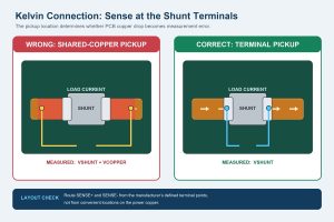
TDR locates impedance changes over time or distance, but launches, coupons, cables, fixtures, calibration, and measurement windows affect results. VNA testing adds frequency-domain reflection and transmission data and also requires defined fixtures and calibration.

Applicable acceptance documents may include IPC-6012F for rigid-board performance, IPC-A-600M for printed-board acceptability, J-STD-001J for soldering process requirements, and IPC-A-610J for completed assembly acceptability. The purchase specification should identify the required revision, class, addenda, and customer-specific criteria.

What Signal Transmission PCB Design and Manufacturing Services Can We Provide?

Support must produce an approval or a verifiable deliverable. Founded in 2006, EBest Circuit supports signal transmission PCB projects from design and prototype through sourcing, assembly, and mass production.

Service stage Engineering work Customer decision or deliverable
PCB design and DFM review Review stackup, controlled nets, reference continuity, differential routing, via transitions, mask, test access, panelization, and conflicting notes Resolved engineering questions and approved design changes before fabrication
Stackup coordination Match requested materials and copper to available cores and prepregs; calculate producible widths and gaps Approved production stackup and impedance geometry
Prototype fabrication Build FR-4, high-speed, high-frequency, impedance-control, HDI, high-Tg, flexible, or rigid-flex prototypes as specified Bare boards and the electrical, impedance, or inspection records named in the order
Component sourcing and PCB assembly Review BOM, approved alternates, sourcing scope, centroid, stencil data, polarity, test access, programming, and handling requirements Assembled boards with agreed inspection, programming, or functional-test records
Impedance verification Test representative coupons against the released target, tolerance, layer, and structure TDR report that identifies each tested impedance class
Production transfer Preserve approved files, material rules, deviations, tests, and change approvals Revision-controlled baseline for mass production and repeat orders
Expedited project review Check stackup, material availability, quantity, assembly scope, testing, and shipping requirements A committed schedule based on the actual build rather than a generic lead-time promise

Define exclusions before quotation. Confirm whether pricing includes design work, component sourcing, fixtures, programming, impedance reports, X-ray, functional testing, packaging, and shipment documents. An unspecified service should not be assumed to be included.

Case Studies: FR4 Signal Transmission PCB Prototype to Mass Production

This is a representative FR-4 production-control scenario. It shows the decisions and records needed from prototype release through repeat production.

Project background: A multilayer FR-4 signal transmission PCB carries differential links, clocks, and mixed-signal interfaces through board-edge connectors. Prototype assembly precedes production release.

Project requirements: The release package identifies controlled nets, impedance targets and tolerances, layer references, component models, maximum pair skew, connector launches, prototype quantity, assembly data, and requested impedance evidence. It also states which material substitutions require approval.

Engineering review: The fabricator checks whether the proposed dielectric thickness and finished copper produce manufacturable widths and gaps. The review flags traces crossing reference voids, layer transitions without nearby return vias, excessive unused via stub, ambiguous solder-mask conditions, and test coupons that do not represent the routed structures.

Prototype controls: The approved stackup, geometry, material rules, coupon design, drill options, assembly drawings, and test procedure form one controlled package. Inspection separates bare-board evidence from assembly and functional results.

Production transfer: Approved revisions, material identity, coupon results, inspection records, and accepted deviations form the production baseline. Review laminate, copper, stackup, drill, component, stencil, or test changes before use.

Customer-verifiable outputs: Specify the approved stackup, resolved engineering questions, material record, electrical test status, impedance report, inspection results, assembly records, and functional data in the purchase specification.

Why Choose Us for Controlled-Impedance PCB Prototyping and Assembly?

Choose a supplier by the risk it removes from your project. EBest Circuit combines experience since 2006 with design, prototyping, sourcing, assembly, and mass-production support. Signal transmission PCB customers can reduce supplier handoffs while keeping technical approvals and acceptance evidence visible.

  • Fewer engineering handoffs: One supplier can coordinate PCB design, prototype fabrication, component sourcing, assembly, and production transfer. This reduces revision mismatches between separate design, board, and assembly vendors.
  • Relevant board technologies: FR-4, multilayer, high-speed, high-frequency, impedance-control, HDI, high-Tg, flexible, and rigid-flex options support different channel, density, thermal, and mechanical requirements.
  • Prototype-to-production continuity: The approved stackup, engineering answers, coupon structures, inspection criteria, and accepted deviations can remain linked to the production revision. This lowers the risk of repeating an obsolete prototype decision.
  • Quality evidence matched to the risk: Buyers can specify electrical testing, TDR reports, AOI, X-ray, programming, or functional testing instead of relying on a general quality claim.
  • Support for regulated purchasing: EBest Circuit lists ISO 9001:2015, IATF 16949, ISO 13485:2016, AS9100D, UL, RoHS, and REACH support. Customers should confirm the current certificate or document, covered site, scope, and revision required for their order.
  • Controlled changes after approval: Material, copper, stackup, geometry, drilling, components, stencil, or test changes can be reviewed before use. This protects signal-integrity assumptions and avoids unapproved substitutions.
  • Practical urgent-build planning: Expedited options can be evaluated against material availability, quantity, assembly scope, testing, and shipping needs. Customers receive a project-specific commitment instead of an unsupported universal lead time.

Customer validation remains essential. Supplier records confirm conformance to released manufacturing requirements; they do not replace system simulation, protocol compliance, environmental qualification, or final product validation.

What Files and Specifications Are Required for a Signal Transmission PCB Quote?

A useful quote needs board, assembly, and test data. A complete signal transmission PCB quotation must identify the physical board, controlled structures, assembly scope, and verification plan. Missing stackup, impedance, or test information can produce a price that does not represent the intended build.

  1. Gerber or ODB++: Include every copper, solder-mask, legend, paste, profile, and mechanical layer with unambiguous layer names. This prevents missing layers, polarity errors, and artwork misinterpretation.
  2. NC drill files: Separate plated and non-plated holes and define slots, blind or buried vias, controlled-depth drilling, and backdrilling. This prevents the wrong via structure, residual stub, or mechanical mismatch.
  3. PCB stackup: State the layer order, finished copper, cores, prepregs, target dielectric thickness, material family, and permitted substitutions. These inputs are required for a valid impedance calculation.
  4. Controlled-impedance table: Identify each net class, single-ended or differential target, tolerance, routing layer, reference layer, mask condition, and coupon requirement.
  5. Fabrication drawing: Define board dimensions, finished thickness, copper, surface finish, solder mask, legend, profile, IPC revision and class, and special acceptance criteria.
  6. BOM and approved sources: Provide manufacturer part numbers, quantities, approved alternates, do-not-substitute parts, and sourcing responsibility. Highlight termination components and connectors that affect channel behavior.
  7. Centroid and assembly drawing: Include reference designators, X/Y coordinates, rotation, board side, polarity, special placement, and manual-assembly instructions.
  8. Test specification: Define the method, fixtures, limits, software, sample plan, calibration, report format, and customer-supplied test assets. State whether TDR, programming, functional testing, or interface validation is required.
  9. Commercial requirements: State prototype and production quantities, panel preference, delivery destination, packaging, revision, and requested schedule. This allows comparable pricing and lead-time review.

  10. Release status: Mark the package as design review or production release, list open decisions, and name the approval authority. This prevents unfinished data from being treated as approved production files.

Mark unfinished layouts as design-review releases and list open decisions. Do not treat a quote based on provisional impedance or material assumptions as production approval.

FAQs About Signal Transmission PCB

Q1: What impedance values are common on a signal transmission PCB?

A1: The interface specification and component guidance determine the required impedance. Single-ended and differential targets vary by protocol, connector, topology, and measurement reference. Do not copy a familiar value into the fabrication notes without identifying the controlled nets, tolerance, layers, and reference planes.

Q2: How should a signal transmission PCB impedance coupon represent production traces?

A2: The coupon should reproduce the controlled structure being accepted. Match the production layer, reference plane, dielectric construction, copper condition, mask condition, and relevant geometry. The drawing should identify which coupon trace corresponds to each impedance class.

Q3: What controlled-impedance tolerance should be specified?

A3: Set the tolerance from interface margin and measurement capability. A tighter number is not automatically better. Confirm whether the limit applies to nominal calculations, production coupons, or routed structures, and define the measurement method before ordering.

Q4: Why do PCB impedance calculators produce different results?

A4: They may use different equations, field solvers, material inputs, and geometry assumptions. Compare design Dk, pressed dielectric height, finished copper, plating, etched shape, solder mask, and frequency. Use the fabricator-approved stackup and correlate critical structures with a representative coupon.

Q5: Can a four-layer signal transmission PCB support controlled impedance?

A5: Yes, when the stackup provides a continuous nearby reference and producible geometry. Confirm dielectric height, finished copper, trace width, pair gap, plane continuity, and transitions with the fabricator. Layer count alone does not determine signal-integrity performance.

Q6: Why can prototype and production impedance results differ?

A6: Material, dielectric thickness, copper, etch, plating, resin flow, coupon design, and measurement setup can vary. Use the same approved construction, documented process controls, representative coupons, and change-approval rules to improve correlation.

Q7: Does length matching guarantee differential-pair signal integrity?

A7: No, length matching controls skew but does not correct impedance, loss, or return-path defects. The pair also needs symmetrical pads and vias, continuous reference planes, controlled coupling, suitable launches, and acceptable insertion and return loss.

Q8: Can a high-speed signal use a power plane as its reference?

A8: It can in a defined structure, but a continuous ground reference is usually easier to control. The power plane must remain continuous and provide a low-impedance high-frequency return relationship. If the reference changes, add an appropriate nearby return connection and validate the transition.

Q9: Does grounded copper beside a controlled trace change its impedance?

A9: Yes, nearby grounded copper can create coplanar coupling and shift the finished impedance. Define the copper gap, via stitching, mask condition, and keep-out in the field-solver model. Avoid uncontrolled or floating copper beside sensitive traces.

Q10: What should be checked after the fabricator changes trace width or pair spacing?

A10: Recheck more than the target impedance before approving the change. Verify clearance, differential coupling, delay, pair skew, pad neck-downs, solder mask, adjacent copper, routing density, and coupon geometry against the released stackup.

Conclusion

Reliability depends on preserving one controlled channel. A signal transmission PCB production release must preserve the approved stackup, geometry, return paths, transitions, assembly data, and acceptance evidence.

For a signal transmission PCB design review, controlled-impedance prototype, bare-board fabrication, PCB assembly, or production quotation, contact EBest Circuit at sales@bestpcbs.com. Send the Gerber or ODB++, NC drill, stackup, and impedance table. Include the fabrication drawing, quantity, BOM, centroid file, assembly drawing, and test requirements for engineering review before quotation.

You may also like

Practical IC Programming Guide for PCBA Assembly and Testing

July 31st, 2026

IC programming is the process of loading firmware, configuration data, or code into an integrated circuit so the assembled product can perform its intended function. In PCB assembly, this step often applies to microcontrollers, memory chips, programmable logic devices, and other programmable ICs used in embedded products.

For engineers and buyers, the real concern is not only “Can this chip be programmed?” It is whether the programming file, IC model, PCB footprint, programming interface, fixture, verification method, and functional test plan can work together during PCBA production. EBest Circuit (Best Technology) supports PCB fabrication, component sourcing, SMT assembly, IC programming coordination, inspection, testing, and small-batch production. If your project needs IC programming during PCBA assembly, please send your Gerber files, BOM, CPL, firmware file, programming notes, and test requirements to sales@bestpcbs.com for engineering review before production.

IC programming
IC programming in PCBA production uses programming fixtures, approved firmware files, and verification steps.

What Is IC Programming in PCB Assembly?

IC programming in PCB assembly means loading customer-provided data or firmware into a programmable IC before shipment or during the PCBA process.

In a PCBA project, IC programming may happen:

  • before SMT, when blank ICs are programmed first
  • after SMT, when the assembled board is programmed through a connector or test pads
  • during functional testing, when programming and verification are combined
  • during rework, when a firmware version needs to be updated

Common programmable ICs include microcontrollers, EEPROM, Flash memory, CPLD, FPGA, and selected communication or control ICs.

The PCB assembly supplier should not create the firmware logic. That belongs to the customer’s engineering team. The supplier’s role is to follow the approved programming file, programming method, fixture requirement, verification step, and production note.

For projects that also involve board-level programming, our related guide on how to program a PCB board explains the broader PCBA programming workflow.

Integrated Circuit Programming vs PCB Programming

Integrated circuit programming and PCB programming are closely related, but they are not always the same thing.

TermPractical Meaning
Integrated circuit programmingLoading data into a specific IC
PCB programmingProgramming an assembled board through the PCB interface
Firmware loadingLoading customer firmware into a device
Functional programmingProgramming followed by board-level function check

For example, an EEPROM may be programmed before assembly. A microcontroller may be programmed after SMT through SWD, JTAG, UART, USB, or test pads. A complete control board may need programming plus functional testing before shipment.

This distinction matters because the production plan changes depending on when the IC is programmed.

If the IC is programmed before SMT, the supplier must control labels, part separation, orientation, and moisture handling. If programming happens after SMT, the PCB must provide access to programming pads, connectors, or fixtures. If programming is part of final test, the test procedure must define pass/fail criteria clearly.

Which ICs Need Programming Before or After Assembly?

Not every IC needs programming. Some components are fixed-function devices. Others must receive firmware, configuration data, calibration data, serial numbers, or customer-specific settings.

Common ICs that may need programming include:

  • microcontrollers
  • EEPROM and Flash memory
  • CPLD and FPGA devices
  • programmable logic ICs
  • motor control ICs with configuration memory
  • communication modules
  • sensor modules with calibration data
  • power management ICs with configurable settings

Before-assembly programming is useful when:

  • the IC cannot be accessed after assembly
  • the board has no programming connector
  • the customer wants programmed parts placed directly
  • the production process uses pre-programmed IC labels

After-assembly programming is useful when:

  • the board has programming pads or connectors
  • the firmware version may change late in the project
  • the product needs board-level verification after programming
  • the same hardware supports multiple firmware versions

For PCBA projects, the safest approach is to confirm the programming stage before SMT starts. A board that is already assembled but has no accessible programming interface can create avoidable rework.

IC Programming Files Customers Should Provide

For IC programming to run smoothly, the programming information must be clear before production.

IC programming
Programming preparation should connect firmware files, BOM, CPL, board revision, and production notes.

Useful files and notes include:

  • firmware file, such as HEX, BIN, ELF, or other approved format
  • exact IC part number
  • BOM and approved alternates
  • programming method
  • programming voltage and interface notes
  • checksum or verification requirement
  • firmware version number
  • security or lock-bit instructions
  • label and traceability requirement
  • functional test procedure
  • pass/fail criteria
  • special handling notes

A file name alone is not enough. For example, `final.hex` does not tell the production team which IC it belongs to, which board revision it matches, or whether the chip should be locked after programming.

A better programming note would include the IC model, board revision, firmware version, programming interface, verification method, and required output label.

If component sourcing is included, the BOM should also show whether ICs are blank, pre-programmed, customer-supplied, or manufacturer-sourced. This is especially important for turnkey PCBA projects involving component sourcing.

IC Programming Methods in PCBA Production

IC programming can be handled in different ways depending on the chip, board layout, quantity, and test requirement.

MethodTypical Use
Offline programmingIC programmed before assembly
In-system programmingIC programmed after assembly
Fixture programmingBoard programmed through test pads
Connector programmingBoard programmed through USB, JTAG, SWD, UART, or other port
Functional test programmingProgramming combined with final test

Offline programming is useful for simple ICs or parts that are hard to access after assembly. In-system programming is common for microcontroller boards because the firmware can be loaded after the board is assembled.

Fixture programming is useful when the product has test pads but no external programming connector. In this case, pad size, pad location, fixture access, and board support must be reviewed before production.

The programming method should be selected by the customer’s engineering team. EBest Circuit can review whether the PCB files, assembly process, fixture access, and testing notes support that approved method.

IC Programming Setup for PCBA Production

A reliable IC programming setup is more than a programmer device. It is a controlled production step.

The setup should define:

  • programming software version
  • programmer model or approved equipment
  • adapter, socket, cable, or fixture
  • IC orientation
  • board power condition
  • connection method
  • firmware version
  • verification step
  • pass/fail output
  • label or record requirement

For assembled boards, the physical access matters. Programming pads should not be blocked by tall components. Test points should not be too small or too close together. If a bed-of-nails fixture is used, the board should have enough support so pogo pins do not bend the PCB during contact.

For boards with BGA, fine-pitch ICs, or dense layouts, programming access should be reviewed together with SMT and inspection requirements. If the project includes complex assembly, BGA assembly and X-Ray inspection may also be part of the production plan.

How to Program an IC During PCBA Assembly

A practical IC programming flow during PCBA assembly usually follows a controlled sequence.

Typical flow:

  • Review customer files and programming notes.
  • Confirm the programmable IC part number and board revision.
  • Check whether programming happens before or after SMT.
  • Prepare firmware file, programmer, cable, fixture, or adapter.
  • Build and inspect the PCBA.
  • Power the board under the approved condition.
  • Load the firmware or data into the IC.
  • Verify checksum, readback, or software confirmation.
  • Run functional test if required.
  • Record version, label, and packing notes.

The most common problems happen when one step is unclear. The IC may be correct, but the firmware version may not match the board revision. The programming port may exist, but the connector may be blocked after enclosure assembly. The board may program successfully, but functional testing may fail because the test procedure is incomplete.

For prototype and small-batch PCBA, the goal is not only to program the IC. The goal is to confirm that the board can be programmed repeatedly, inspected clearly, and tested before delivery.

Programmed IC Verification and Functional Testing

Programming is not complete until the result is verified.

IC programming
Programmed IC verification and functional testing help confirm the board is ready before delivery.

Useful verification methods include:

  • checksum verification
  • readback comparison
  • programmer software confirmation
  • power-on check
  • LED or display response
  • communication test
  • sensor or input/output test
  • current consumption check
  • customer-defined functional test

For production, verification should be documented clearly. A message that says “programming successful” may not be enough if the customer also requires communication, calibration, output control, or serial number confirmation.

For PCBA projects, EBest Circuit can coordinate programming with inspection and testing requirements. Depending on the project, this may include AOI, X-Ray, visual inspection, electrical testing, functional testing, labeling, and packing.

This is useful for prototype PCB assembly because early builds often reveal whether the programming interface, firmware version, test fixture, and final inspection method are ready for the next production stage.

IC Programming Services Case Study for a PCBA Project

A European customer needed a small-batch PCBA for an industrial control product. The board used a programmable microcontroller, several communication interfaces, connectors, and customer firmware that had to be loaded after SMT assembly.

Project requirements:

  • Customer region: Europe
  • Application: industrial control module
  • Build stage: prototype to small-batch validation
  • PCB type: multilayer FR4 PCBA
  • Assembly: SMT plus connector assembly
  • Programming: customer-provided firmware loaded after SMT
  • Testing: programming verification and functional test
  • Packing: single-board protection for delivery

Main challenge:

The board itself was not difficult only because of SMT. The real risk was the handoff between files, components, programming, testing, and shipment. If the firmware version, board revision, connector direction, programming pads, or test steps were unclear, the customer could receive boards that looked complete but were not ready for system validation.

EBest Circuit’s production support:

  • Reviewed Gerber, BOM, CPL, and assembly drawing together.
  • Confirmed the microcontroller part number and programming interface.
  • Checked connector orientation and programming access before SMT.
  • Loaded the customer-provided firmware after assembly.
  • Verified the programming result before functional test.
  • Kept firmware version and packing notes visible until shipment.

Result:

The customer received programmed PCB assemblies ready for engineering validation. The useful value was not only loading firmware into the IC. It was keeping PCB fabrication, SMT assembly, IC programming, testing, and delivery notes connected in one workflow.

For customers comparing IC programming services, this kind of coordination reduces the risk of “assembled but not usable” boards.

FAQs About IC Programming

1. What is IC programming? IC programming is the process of loading firmware, data, or configuration information into an integrated circuit, such as a microcontroller, EEPROM, Flash memory, CPLD, or FPGA.

2. Is IC programming the same as PCB programming? Not exactly. IC programming focuses on a specific chip. PCB programming usually means programming the assembled board through a connector, test pads, or programming interface.

3. Can EBest Circuit write the firmware for my IC? No. The firmware logic and program content should come from the customer’s engineering team. EBest Circuit can help load customer-provided firmware during PCBA assembly and coordinate verification or functional testing.

4. What files are needed for IC programming? Common files include HEX, BIN, or another approved programming file, plus IC part number, board revision, programming method, checksum requirement, firmware version, and test instructions.

5. Should IC programming happen before or after SMT assembly? It depends on the IC, PCB layout, programming access, firmware stability, and test plan. Some ICs are programmed before assembly. Many microcontroller boards are programmed after SMT through a connector, pads, or fixture.

All in all, IC programming should be planned as part of the PCBA production path, not treated as a last-minute task after assembly. If your project needs IC programming, firmware loading, programming pads, test fixtures, functional testing, or small-batch PCBA support, please send your Gerber files, BOM, CPL, firmware file, and programming notes to sales@bestpcbs.com. EBest Circuit can help review whether the manufacturing and assembly path is ready before production starts.

You may also like

PCB Transformer Guide for Layout and PCBA Assembly

July 31st, 2026

A pcb transformer can mean different things in electronics manufacturing. In most PCB and PCBA projects, it refers to a transformer mounted on a printed circuit board, or a transformer structure that is integrated into the board design for voltage conversion, isolation, signal coupling, or power regulation.

For engineers and buyers, the real question is not only “what transformer should I use?” The bigger production question is whether the PCB layout, copper design, clearance, creepage, soldering process, mechanical support, BOM, and inspection plan can support the transformer safely and repeatably.

pcb transformer
PCB transformer projects should be reviewed as complete PCB and PCBA builds, not only as transformer component choices.

EBest Circuit (Best Technology) supports PCB fabrication, BOM review, component sourcing, SMT assembly, through-hole assembly, mixed PCBA production, inspection, and testing coordination for transformer-related PCB and PCBA projects. If your project includes PCB-mounted transformers, planar transformers, isolation transformers, or power transformer circuits, our team can review the manufacturing files and assembly requirements before production.

What Is a PCB Transformer?

A PCB transformer is usually a transformer used on a printed circuit board. It may be a discrete PCB mount transformer soldered onto the board, or a transformer structure created with copper windings, magnetic cores, and insulation features in the PCB design.

In this article, PCB means printed circuit board. It does not refer to PCB chemicals in transformer oil, disposal, contamination, or environmental regulations.

In electronics, a PCB transformer is commonly used for:

  • Voltage step-down or step-up
  • Electrical isolation between input and output circuits
  • Signal coupling
  • Noise reduction
  • Impedance matching
  • Power conversion in compact products
  • Safety separation in control and power boards

A PCB transformer can appear in power adapters, industrial controllers, LED drivers, communication equipment, medical electronics, automotive modules, energy storage devices, and other products where controlled power transfer or isolation is required.

For production teams, the transformer is not only a component on the BOM. It affects the board layout, copper thickness, thermal behavior, assembly method, solder joint strength, inspection plan, and final test requirements.

PCB Mount Transformer vs Transformer Built Into a PCB

A PCB mount transformer and a transformer built into a PCB are related, but they are not the same manufacturing situation.

Type What It Means Main Manufacturing Focus
PCB mount transformer A finished transformer component soldered onto the PCB Footprint, pin fit, soldering, height, clearance, mechanical support
Through-hole transformer A larger transformer with pins inserted through plated holes Hole size, annular ring, solder fill, board support, wave or hand soldering
SMT transformer A surface-mount transformer placed by SMT process Pad design, solder paste, reflow profile, coplanarity, AOI limits
Planar transformer PCB Windings are formed by PCB copper layers Stackup, copper thickness, insulation, alignment, thermal path
Transformer circuit board A board that carries transformer-related power or isolation circuits Creepage, clearance, copper width, slots, testing, safety documentation

A PCB mount transformer is usually easier for buyers to source because it is a standard component. The customer provides the transformer part number, datasheet, BOM, Gerber files, and assembly drawing. The PCBA supplier then checks whether the footprint, soldering process, and board design are manufacturable.

A planar transformer PCB is more demanding. The PCB itself becomes part of the magnetic structure, so copper thickness, layer registration, dielectric thickness, insulation spacing, and process tolerance become more critical.

For EBest Circuit, the correct role is manufacturing and assembly support. We can review whether the PCB and PCBA files are suitable for production, but the customer’s engineering team should define the transformer electrical design, safety standard, magnetic design, and approved component specification.

How Does a Transformer on Circuit Board Work?

A transformer on circuit board works by electromagnetic induction. The primary side receives an AC or switching signal. The changing current creates magnetic flux, and the secondary side receives induced voltage through magnetic coupling.

In practical PCB projects, the transformer may work in different ways depending on the circuit:

  • In an AC-DC power board, it may step down voltage and provide isolation.
  • In a flyback converter, it may store and transfer energy between switching cycles.
  • In a signal isolation circuit, it may transfer signals while separating grounds.
  • In a communication circuit, it may support impedance matching and noise control.
  • In a current sensing design, it may help measure current without direct electrical connection.

The PCB layout around the transformer matters because high voltage, high current, switching noise, and heat can all concentrate in the same area.

Key production-related risks include:

  • Primary and secondary spacing is too small.
  • Copper width is not enough for current.
  • Thermal relief affects soldering or heat flow.
  • Transformer body blocks nearby inspection points.
  • Tall components interfere with enclosure clearance.
  • Pin pitch does not match the actual transformer datasheet.
  • Silkscreen or polarity marks are unclear.
  • Slots, cutouts, or keepout zones are missing.

A transformer can be electrically correct in the schematic but difficult to build if the PCB and assembly details are not controlled early.

PCB Transformer Board Requirements Before Production

Before a PCB transformer board enters production, the PCB supplier should not only look at board size, layers, and quantity. The board needs a manufacturing review around power, isolation, heat, and assembly risk.

Key files to prepare before quotation:

  • Gerber files
  • NC drill file
  • PCB stackup
  • Finished copper thickness
  • Board thickness
  • Surface finish
  • BOM
  • Pick-and-place file
  • Assembly drawing
  • Transformer datasheet
  • Safety or creepage requirements if applicable
  • Test procedure if PCBA testing is required

For transformer-related PCB boards, several areas deserve special attention.

Clearance and creepage

Clearance is the direct air distance between conductive parts. Creepage is the distance along the board surface. Transformer circuits may require larger spacing between primary and secondary sides, especially when the board handles AC input, high voltage, or safety isolation.

If the design needs slots, isolation grooves, wider spacing, or special coating, these requirements should be shown clearly in the fabrication notes.

Copper width and copper weight

Transformer circuits often carry higher current than small signal circuits. Copper width, copper thickness, via count, and thermal path should match the current and heat requirement. If copper is too narrow, the board may pass initial testing but run hot during long operation.

Hole and pad reliability

For through-hole transformers, plated through holes need proper hole size, annular ring, solderability, and mechanical strength. Large transformer pins, thick leads, or heavy bodies can create stress during insertion, soldering, transportation, or product use.

Board material and thickness

Most transformer carrier boards use FR4, but high-temperature, high-current, or compact power designs may need higher Tg material, heavier copper, or special stackup review. For planar transformer PCBs, dielectric thickness and copper layer structure become part of the design result.

Marking and orientation

Transformer direction, pin 1, primary side, secondary side, and polarity marks should be visible on the silkscreen or assembly drawing. Ambiguous marking can cause assembly mistakes, especially in mixed SMT and through-hole production.

How to Control PCB Transformer Assembly and Inspection Quality?

PCB transformer assembly quality depends on the transformer package, weight, pin type, soldering method, and how the board will be used after shipment.

pcb transformer
PCB transformer assembly quality depends on footprint fit, soldering process, inspection access, and functional test planning.

For SMT transformers, the main risks are solder paste volume, pad design, component shift, reflow profile, and hidden solder joint defects. For through-hole transformers, the main risks are hole fit, solder fill, pin wetting, flux residue, and mechanical stress.

Important assembly checks include:

  • Confirm transformer part number against BOM and datasheet.
  • Check package size, pin pitch, and mounting direction.
  • Verify polarity and primary/secondary orientation.
  • Review solder paste opening for SMT transformer pads.
  • Confirm through-hole pin insertion and solder fill.
  • Inspect heavy transformer body support.
  • Check clearance around heat-sensitive plastic parts.
  • Review wave soldering or selective soldering feasibility.
  • Confirm AOI visibility and manual inspection points.
  • Add functional testing when the customer provides test procedures.

A transformer may be too tall or too heavy for a weak board support area. If the product will face vibration, transportation shock, or repeated plug-in force nearby, mechanical review is important. In some projects, adhesive, extra fixture support, conformal coating, or mechanical fasteners may be needed, depending on customer drawings and product requirements.

For PCBA inspection, AOI is helpful but not enough for every transformer assembly. Large bodies can block solder joints. Through-hole solder joints may require visual inspection from both sides. Functional testing is often more useful when the board includes voltage conversion, isolation, or power output requirements.

EBest Circuit can support inspection planning based on customer files, including AOI, visual inspection, X-ray when applicable, and functional testing coordination when test instructions and fixtures are provided.

Planar Transformer PCB Requirements for High-Frequency Power Boards

A planar transformer PCB is different from a normal board carrying a transformer component. In a planar transformer design, the PCB copper layers form transformer windings. This makes PCB fabrication quality directly affect electrical behavior.

pcb transformer
Planar transformer PCB fabrication requires controlled copper geometry, dielectric spacing, and clear manufacturing notes.

Planar transformer PCB projects are commonly used in high-frequency power supplies, compact DC-DC converters, telecom power modules, EV-related electronics, industrial power boards, and other products where space, efficiency, and repeatability matter.

Planar transformer PCB requirements often include:

  • Controlled PCB stackup
  • Stable dielectric thickness
  • Accurate layer registration
  • Suitable copper thickness
  • Clear winding geometry
  • Reliable via structure
  • Consistent insulation spacing
  • Good thermal path
  • Clean routing between primary and secondary areas
  • Clear fabrication notes

The manufacturing risk is higher because small changes in copper geometry, dielectric spacing, or layer alignment can affect performance. The PCB supplier should review whether line width, spacing, copper thickness, drilling, lamination, plating, and routing requirements match the actual manufacturing capability.

For buyers, the RFQ should not only say “planar transformer PCB.” It should include stackup, copper weight, material, insulation requirement if needed, working voltage, board thickness, surface finish, and any special acceptance criteria.

EBest Circuit can review planar transformer PCB fabrication files from a manufacturability perspective and advise whether the structure fits available PCB process capability.

Power Transformer PCB Risks Buyers Should Confirm Before RFQ

A power transformer PCB is often part of a product where heat, current, safety, and reliability are more important than simple board cost.

Buyers should confirm several practical risks before sending an RFQ.

Project requirements:

  • Input and output voltage range
  • Current and power rating
  • Transformer part number or approved alternatives
  • PCB copper thickness
  • Minimum clearance and creepage
  • Board material and Tg requirement
  • Thermal management requirement
  • Assembly method
  • Inspection standard
  • Functional test requirement
  • Coating or potting requirement
  • Delivery schedule and quantity

Common quotation problems:

  • Transformer datasheet is missing.
  • BOM part number does not match the footprint.
  • Gerber files do not show enough isolation spacing.
  • Copper thickness is not specified.
  • Assembly drawing does not show transformer direction.
  • High-current nets are not clearly marked.
  • Testing requirement is discussed only after assembly.
  • Coating or potting is requested after quotation.
  • Packaging requirements are not defined for tall components.

For production, these details affect cost and lead time. A board with a large through-hole transformer may need different soldering control than a compact SMT board. A power board with high current may need thicker copper or wider traces. A board with safety isolation may need larger spacing, slots, or clearer documentation.

A good supplier should help identify these manufacturing risks before production, not after the first batch fails inspection.

How EBest Circuit Supports PCB Transformer Projects

EBest Circuit (Best Technology) supports PCB transformer projects from PCB fabrication to PCBA assembly when customers provide the approved design files, BOM, transformer specifications, and production requirements.

EBest Circuit supports transformer-related PCB and PCBA projects with:

  • PCB fabrication for FR4, multilayer, heavy copper, high Tg, and special PCB requirements
  • DFM review for manufacturability before production
  • BOM review and component sourcing support
  • SMT assembly for surface-mount transformer and related components
  • Through-hole assembly for larger PCB mount transformers
  • Mixed assembly for power boards with SMT and THT components
  • AOI and visual inspection
  • X-ray inspection when applicable
  • Functional testing coordination based on customer test instructions
  • Prototype, small-batch, and production support

For transformer-related boards, our engineering review can help check whether the PCB layout, hole size, copper thickness, soldering process, component spacing, and assembly notes are clear enough for production.

EBest Circuit does not replace the customer’s electrical design team. The customer should define the transformer electrical specification, magnetic design, safety standard, and final performance targets. Our value is helping turn approved design files into reliable PCB and PCBA production with practical manufacturing control.

If your PCB or PCBA project includes PCB-mounted transformers, planar transformer structures, high-current power sections, or isolation circuits, send your files to sales@bestpcbs.com for engineering review and quotation.

PCB Transformer Case Example for a Power Control Board

A European industrial equipment customer prepared a small-batch power control board for a 24 V control system. The board included a through-hole PCB mount transformer, relays, terminal blocks, fuses, electrolytic capacitors, and mixed SMT control components.

Project requirements:

  • Country: Germany
  • Quantity: 120 pcs pilot run
  • Application: industrial control power module
  • Board type: FR4 multilayer PCB with mixed SMT and through-hole assembly
  • Key component: through-hole PCB mount transformer
  • Delivery requirement: pilot batch for functional validation

The first concern was not whether the transformer could be purchased. The real production issue was whether the board could be assembled and inspected reliably.

Main challenges:

  • The transformer body was tall and heavier than surrounding components.
  • Primary and secondary areas needed clear separation.
  • The transformer pins required stable solder fill.
  • The BOM had one alternate transformer with slightly different pin dimensions.
  • The assembly drawing did not clearly mark the transformer orientation.
  • The customer needed functional testing after assembly.

During DFM and assembly review, EBest Circuit checked the transformer footprint, pin hole size, soldering method, component keepout area, and inspection accessibility. The BOM was reviewed against the transformer datasheet, and the alternate part was flagged for confirmation before sourcing.

EBest Circuit solution:

  • Confirmed transformer footprint and pin spacing before production
  • Reviewed hole size and annular ring for through-hole soldering
  • Checked spacing around transformer primary and secondary areas
  • Recommended clearer assembly marking for transformer orientation
  • Coordinated SMT and through-hole assembly sequence
  • Added manual inspection for transformer solder joints
  • Followed customer-provided functional test steps after assembly
  • Packed the boards with protection for tall components

This type of project shows why a PCB transformer board should not be treated like a simple bare PCB order. The transformer affects fabrication, assembly, inspection, testing, and packaging. When those details are reviewed before production, buyers have fewer surprises during pilot build and batch delivery.

FAQs About PCB Transformer

What is a PCB transformer?

A PCB transformer is a transformer used on or built into a printed circuit board. It may be a PCB mount transformer component or a transformer structure created with PCB copper windings and magnetic core materials.

Is a PCB transformer the same as PCB transformer oil?

No. In electronics manufacturing, PCB means printed circuit board. PCB transformer oil usually refers to polychlorinated biphenyl contamination or environmental disposal topics, which are not the same as PCB and PCBA manufacturing.

Can EBest Circuit manufacture transformer components?

EBest Circuit supports PCB fabrication, component sourcing, PCBA assembly, inspection, and testing coordination. We do not claim to design or manufacture transformer magnetic components themselves. Customers should provide approved transformer part numbers, datasheets, and design requirements.

What files are needed for a PCB transformer PCBA quote?

Please provide Gerber files, NC drill files, BOM, pick-and-place file, assembly drawing, transformer datasheet, quantity, surface finish, copper thickness, testing requirements, and delivery target.

Why is clearance and creepage important on a PCB transformer board?

Transformer circuits may separate high-voltage and low-voltage areas. Proper clearance and creepage help reduce arcing, leakage, and insulation risk. The required spacing depends on the product standard, voltage, environment, and design requirement.

In Conclusion, a pcb transformer project should be reviewed as a complete PCB and PCBA manufacturing task, not only as a transformer component selection issue. The transformer affects layout spacing, copper design, thermal behavior, soldering, inspection, testing, and packaging.

EBest Circuit (Best Technology) supports PCB fabrication, DFM review, component sourcing, PCBA assembly, inspection, and testing coordination for transformer-related PCB projects. To review your Gerber files, BOM, transformer datasheet, assembly drawing, and production requirements, contact sales@bestpcbs.com.

You may also like

How to Read the 4.7k Resistor Color Code and Verify It on a PCB

July 31st, 2026

The standard four-band 4.7k resistor color code is yellow-violet-red-gold. Yellow represents 4, violet represents 7, red supplies the ×100 multiplier, and gold specifies ±5% tolerance. The result is 47 × 100 = 4,700Ω, which is also written as 4.7kΩ or 4k7.

Visual decoding is only the first verification step. Band direction, tolerance, heat discoloration, conformal coating, similar resistance values and parallel PCB paths can all affect the decision. Confirm the value against the schematic and BOM, remove power, discharge stored energy and isolate one resistor lead when an in circuit measurement is inconclusive.

4.7k resistor color code on an axial resistor beside an assembled PCB

What Is the Correct 4.7k Resistor Color Code?

A common four-band 4.7kΩ ±5% resistor uses yellow, violet, red and gold. The first two bands are the significant digits, the third is the multiplier and the fourth is the tolerance. Reading the colors in the wrong direction or confusing red with orange changes the decoded value by a factor of ten.

Band Color Meaning Result
1 Yellow First digit 4
2 Violet Second digit 7
3 Red Multiplier ×100
4 Gold Tolerance ±5%

The nominal resistance is calculated before tolerance is applied. Yellow and violet form 47; red multiplies 47 by 100 to produce 4,700Ω. Gold does not change the nominal value. It defines how far a new resistor may deviate from 4,700Ω under the specified measurement conditions.

Not every 4.7kΩ resistor ends with a gold band. Brown commonly indicates ±1%, red ±2% and silver ±10%. The tolerance band must therefore be decoded separately from the value bands. Package size, power rating and resistor technology cannot be determined from the four value and tolerance colors alone.

Color decoding also cannot distinguish a carbon film part from a metal film or flameproof resistor with complete certainty. Body color and surface finish vary by manufacturer. When noise, pulse loading, safety behavior or long term drift matters, use the full manufacturer part number rather than treating the band sequence as a complete specification.

How Should You Determine the Correct Reading Direction for a 4.7k Resistor Color Code?

Begin at the end where the significant digit bands are grouped more closely together. On many four-band axial resistors, the gold or silver tolerance band is separated by a wider gap and belongs on the right. Five- and six-band parts require more care because both end bands may use ordinary colors.

  1. Inspect the spacing. Look for a wider gap before the final tolerance or temperature-coefficient band.
  2. Check the end color. Gold and silver are normally tolerance colors and do not serve as significant digits.
  3. Decode both directions. Compare the resulting values and reject an orientation that produces an invalid or implausible band role.
  4. Compare the circuit record. Match the result with the reference designator, schematic function, BOM value and approved part number.
  5. Measure when uncertain. Use resistance mode on an unpowered circuit and isolate the component if connected paths affect the result.

Use neutral white lighting and magnification when the colors are unclear. Heat can darken a resistor body, flux residue can add a yellow-brown tint, and conformal coating can create reflections. Do not scrape the coating or damage the resistor merely to improve the view; electrical verification is safer when visual evidence remains ambiguous.

Observation Likely Meaning Next Check
Gold or silver band isolated at one end That end is normally the tolerance side Read from the opposite end
Both directions produce plausible values Visual direction remains uncertain Compare BOM, schematic and measurement
Band colors change with viewing angle Coating reflection or poor lighting Use neutral light and magnification
Body or bands are darkened by heat Value and condition cannot be trusted visually Inspect the circuit and isolate the part

How Do 4‑Band, 5‑Band and 6‑Band Color Codes Represent 4.7kΩ?

Four band codes use two significant digits, while five and six band codes normally use three. A five band 4.7kΩ resistor is decoded as 470 × 10. A sixth band usually adds temperature coefficient information rather than another resistance digit.

Format Typical Sequence Calculation Final Band Role
4-band Yellow, violet, red, gold 47 × 100 = 4,700Ω Gold: ±5%
5-band Yellow, violet, black, brown, brown 470 × 10 = 4,700Ω Brown: ±1%
6-band 5-band value plus TCR band 470 × 10 = 4,700Ω Temperature coefficient

The common five band ±1% sequence is yellow, violet, black, brown and brown. Yellow, violet and black form 470; the first brown band multiplies by 10; the last brown band specifies ±1%. The physical spacing between the multiplier and tolerance bands helps distinguish their roles.

A six band part can add temperature coefficient in parts per million per degree Celsius. That parameter matters in precision dividers, measurement circuits and bias networks that operate across a wide temperature range. Confirm the exact sixth band meaning in the component documentation because the band count does not prove pulse capability, working voltage or long term stability.

A sixth band does not automatically make the component more accurate. A six band resistor can have a wider initial tolerance than another five band part, while providing additional temperature information. Compare the tolerance band, TCR band and datasheet together instead of ranking components by band count.

What Does IEC 60062 Specify About 4.7k Resistor Color Codes?

IEC 60062:2016 with Amendment 1:2019 specifies designation and marking codes for resistor values, tolerances and temperature coefficients. It covers color coding and letter-and-digit forms used to communicate resistance values. The standard explains the marking system; it does not certify that a particular resistor meets every electrical or reliability requirement.

Under the color-code method, each color has a defined digit or multiplier role. IEC 60062 also supports resistance notations that replace a decimal point with a multiplier letter. This makes 4k7 easier to read than a small printed decimal in many schematics and BOMs. Fixed-length numerical markings can express resistance values on suitable components.

IEC 60062 does not establish the actual power rating, maximum working voltage, pulse endurance or operating temperature limit of an unidentified resistor. Those parameters come from the applicable component specification and manufacturer datasheet. IEC 60115‑1:2020 supplies generic terms, inspection procedures and test methods for fixed resistors, but the relevant sectional or detail specification still controls acceptance.

Assembly requirements have a separate purpose. IPC J‑STD‑001J addresses soldering materials and process requirements, while IPC‑A‑610J addresses completed assembly acceptability. Neither proves that a visually correct resistor is electrically 4.7kΩ. BOM control, material identity and an appropriate electrical or functional test are still required.

IEC 60063:2015 has a related but different role: it defines preferred number series for resistors and capacitors. The presence of 4.7 in a preferred series explains the widespread nominal value, but it does not prove the tolerance or condition of an installed component. Marking, preferred value and component performance remain separate acceptance questions.

For production records, identify the standard by revision instead of writing only “per IEC” or “per IPC.” Also record the approved manufacturer part number and datasheet revision. Add any customer specific acceptance criteria separately. This prevents a marking standard from being misused as evidence for power, reliability or assembly quality.

What Resistance Range Does Each 4.7k Resistor Tolerance Allow?

Tolerance converts the nominal 4,700Ω value into an allowable resistance interval. Multiply 4,700Ω by the tolerance percentage, then subtract and add that deviation. Meter accuracy, lead contact, temperature and the component’s specified test conditions must be considered before accepting or rejecting a measured value.

Tolerance Band Minimum Maximum Typical Decision Use
±10% Silver 4,230Ω 5,170Ω Noncritical legacy or general purpose circuits
±5% Gold 4,465Ω 4,935Ω General pullups and nonprecision networks
±2% Red 4,606Ω 4,794Ω Moderate accuracy requirements
±1% Brown 4,653Ω 4,747Ω Precision bias or divider networks
±0.5% Green 4,676.5Ω 4,723.5Ω Tighter measurement and control circuits

For example, ±5% of 4,700Ω is 235Ω, so the allowed interval is 4,465Ω to 4,935Ω. A reading of 4.82kΩ can pass a ±5% requirement but fail a ±1% requirement. The BOM and tolerance band must therefore be known before the same measured value is judged acceptable.

Tolerance is not the same as temperature coefficient or aging stability. A resistor can begin inside its room temperature tolerance and move with temperature or long term stress. For accuracy-sensitive circuits, check initial tolerance, TCR, environmental range, load life performance and any ratio matching requirement together.

Measurement uncertainty must be applied to the instrument result, not ignored after the tolerance calculation. If a meter specifies accuracy as a percentage of reading plus a number of display counts, both terms affect a borderline result. Clean probe contact and a stable temperature are also necessary before a component near the limit is rejected.

How Can You Distinguish a 4.7k Resistor Color Code from 470Ω and 47kΩ?

The multiplier band separates 470Ω, 4.7kΩ and 47kΩ. All three values begin with the digits 4 and 7, but brown multiplies by 10, red by 100 and orange by 1,000. One multiplier-color error changes resistance by a factor of ten.

Resistance Value Bands Multiplier SMD Code
470Ω Yellow, violet, brown ×10 471
4.7kΩ Yellow, violet, red ×100 472
47kΩ Yellow, violet, orange ×1,000 473

Red and orange are easily confused under warm light or a tinted coating. Compare the resistor with a neutral color reference, then use a resistance measurement if the decade remains uncertain. An isolated reading near 470Ω, 4.7kΩ or 47kΩ normally separates these values clearly.

An assembled board requires additional caution because a parallel path can pull a 4.7kΩ reading below its tolerance range. A low in circuit result does not automatically identify a 470Ω part. Review the schematic and lift one terminal before deciding that the wrong decade was assembled.

The electrical consequence of a decade error depends on the circuit. With a 3.3V open-drain line held low, ideal pull-up currents are about 7.02mA for 470Ω, 0.702mA for 4.7kΩ and 0.0702mA for 47kΩ. The wrong value can therefore overload a driver or create an excessively slow rising edge.

Bus capacitance makes the difference visible in timing. With a simplified 200pF RC load, the time constant is 94ns for 470Ω, 940ns for 4.7kΩ and 9.4µs for 47kΩ. For I²C, the 30%–70% rise time is approximately 0.8473 × RP × CB, so selection must also satisfy the bus mode rise time limit and the device’s low level sink current limit.

How Do 4k7, 4700Ω, 472 and 4701 Represent a 4.7k Resistor?

All four forms can represent the nominal value 4,700Ω. The formats serve different records and component types. Schematics and BOMs commonly use 4k7, while 4700Ω states the full value. Suitable SMD packages may carry the top marking 472 or 4701.

Marking Calculation Common Context Limitation
4k7 4.7kΩ Schematic or BOM Does not state tolerance by itself
4700Ω 4,700Ω Datasheet or test record Requires a separate rating specification
472 47 × 10² Three digit SMD code Small packages may be unmarked
4701 470 × 10¹ Four-digit SMD code Does not prove power or technology

The letter in 4k7 replaces the decimal point, reducing the risk that a faint dot will be missed. In the three-digit SMD code 472, the first two digits are 47 and the final digit indicates two zeros. In 4701, the first three digits are 470 and the last digit applies a ×10 multiplier.

Do not infer an unmarked SMD resistor value from its pad size or location. Confirm the reference designator, approved BOM, reel label, feeder setup and placement record. Use electrical measurement or functional test when production evidence does not resolve the identity.

During purchasing, keep the engineering value and the orderable part number in separate BOM fields. The engineering value may read 4k7, while the manufacturer part number defines package, tolerance, power, TCR and termination. Converting every field to “472” can remove information and increase substitution risk.

Why Can a 4.7k Resistor Show an Incorrect Reading on a PCB?

A meter connected across an installed resistor measures every conductive path between its probes, not only the resistor body. Parallel resistors, IC inputs, protection devices, semiconductor junctions and connected modules can reduce or destabilize the displayed value. Capacitors can create a changing reading as the meter’s test current charges them.

  • Parallel resistance: another path between the same nodes makes the measured value lower than the isolated resistor.
  • Semiconductor conduction: meter polarity and test voltage can forward bias a junction and alter the result.
  • Stored charge: capacitors can create drift and may leave unsafe residual voltage on the assembly.
  • Probe contact: oxidation, flux, coating or unstable pressure can produce intermittent or high readings.
  • Wrong test state: an energized board can damage the meter or assembly when resistance mode is used.
  • Damaged interconnect: a cracked lead, lifted pad or broken trace can imitate an open resistor.

A lower than expected in circuit reading is common because parallel paths reduce total resistance. A reading above the allowed range is more suspicious, but it still requires contact and interconnect checks. Reverse the probes when semiconductor paths are suspected and compare the result with the schematic before isolating the component.

A simple parallel path shows the scale of the error. A correct 4.7kΩ resistor in parallel with 10kΩ produces approximately 3.20kΩ at the same two nodes. That reading is predictable from the circuit and does not indicate that the 4.7kΩ component has changed value.

A drifting display often indicates capacitance rather than an unstable resistor. The meter injects a small test current, causing the capacitor voltage and displayed resistance to change. Disconnect power, discharge the capacitor safely and wait for the reading to settle before deciding whether component isolation is necessary.

An open display can come from a failed resistor, but it can also result from a cracked lead, damaged via, lifted pad or poor probe contact. Probe directly on the resistor leads when accessible, then compare that result with pad to pad and trace measurements. The difference identifies whether the failure is inside the component or in the interconnect.

How Should You Test a 4.7k Resistor In‑Circuit and Out‑of‑Circuit?

Screen the resistor on the unpowered PCB, then lift one lead only when connected paths prevent a reliable decision. Power must be removed and stored charge discharged before resistance testing, as specified in Fluke’s resistance measurement procedure.

  1. Make the board safe. Disconnect power, batteries, programmers and powered cables. Confirm zero voltage at the test nodes and discharge relevant capacitors.
  2. Identify and inspect the part. Match the reference designator to the schematic and BOM. Check the body, leads, solder joints, pads and nearby components for damage or contamination.
  3. Measure in circuit. Select resistance mode or autorange, contact both resistor terminals and avoid adjacent pads. Record a stable, low, high, open, drifting or polarity-dependent result.
  4. Account for connected paths. Compare the reading with parallel resistors, IC inputs, protection devices and capacitors shown on the schematic. A low or changing value may be a network effect.
  5. Isolate only when necessary. Lift one lead with a controlled rework process if the circuit prevents a clear conclusion. Do not cut a lead or overheat the pad for convenience.
  6. Measure the isolated resistor. Allow the part to cool, clean the contact points and compare the stable reading with the specified tolerance range and meter uncertainty.
  7. Restore and verify the assembly. Resolder the lead, inspect wetting and pad condition, then repeat the resistance check and the circuit function affected by the resistor.
Out-of-circuit test of a 4.7k resistor with probes contacting both leads

An isolated ±5% part should read 4.465kΩ to 4.935kΩ; an isolated ±1% part should read 4.653kΩ to 4.747kΩ. Apply the BOM tolerance and the meter’s uncertainty before accepting a borderline value.

Continuity mode is not a resistance-value test. Its threshold varies by meter, so a beep or silence cannot establish 4.7kΩ, tolerance or component condition.

What Evidence Confirms Whether a 4.7k Resistor Passes or Fails?

A pass decision requires a stable isolated value within the specified tolerance, valid material records and a successful circuit level check. An in circuit reading alone is screening evidence because the meter may include other conductive paths.

Observed Result Likely Explanation Required Action
Stable value inside the isolated tolerance range Resistor value is consistent with its marking Restore the joint and perform the circuit test
Stable low value only in circuit Parallel network path Calculate the network or lift one lead
Reading rises or falls Capacitor charging or semiconductor behavior Discharge, reverse probes and review the schematic
Open at pads but correct on resistor leads Joint, pad, via or trace failure Inspect and repair the interconnect
Stable isolated value outside tolerance Wrong value, damage or excessive drift Verify part identity and replace with an approved part

Four-wire measurement is rarely necessary at 4.7kΩ because test-lead resistance is small relative to the component value. For formal acceptance, record the meter model, calibration status, range, stated accuracy, measured value and test temperature.

PCB inspection process used with BOM and electrical testing to verify a 4.7k resistor

For production, the approved BOM and reel label establish material identity; placement records and AOI verify location and visible markings; ICT, flying-probe or functional testing supplies electrical evidence. Test limits must account for parallel paths, and functional coverage must exercise the affected pull-up, bias, divider or timing node.

FAQs About 4.7k Resistor Color Codes

Q1: Does a 4.7kΩ resistor have polarity?

A1: A standard fixed resistor is nonpolarized. Either lead may face either circuit node, although consistent band orientation improves inspection and manual identification.

Q2: Can two series resistors replace one 4.7kΩ resistor?

A2: Series values may total 4.7kΩ, but the substitution requires engineering approval. Combined tolerance, voltage distribution, power dissipation, footprint, creepage and added solder joints can change reliability.

Q3: Can parallel resistors be used to obtain 4.7kΩ?

A3: Yes, if the calculated parallel value and worst-case tolerance meet the circuit requirement. Verify each resistor’s power, the combined footprint and failure behavior before changing the BOM.

Q4: Can a potentiometer adjusted to 4.7kΩ replace a fixed resistor?

A4: Only when adjustability, wiper failure and drift are acceptable. A potentiometer adds mechanical variability, a different footprint and a possible open wiper failure mode that a fixed resistor does not have.

Q5: Can an SMD resistor replace an axial 4.7kΩ resistor?

A5: Only after electrical, thermal and mechanical review. The replacement must satisfy resistance, tolerance, voltage, pulse energy, power derating, land pattern and rework requirements.

Q6: How can a color-blind technician identify the bands?

A6: Use a calibrated color-identification aid and confirm the value electrically. A BOM, reference designator and isolated resistance measurement are more reliable than unaided color judgment.

Q7: Can an axial 4.7kΩ resistor be mounted vertically?

A7: Yes, when the approved footprint and assembly requirements permit it. Check component height, lead forming radius, mechanical support, electrical clearance and vibration exposure.

Q8: Can a resistor pass an ohmmeter test but fail during operation?

A8: Yes, a room-temperature resistance check does not test every stress. Pulse overload, excessive working voltage, intermittent leads, thermal drift or moisture damage may appear only under operating conditions.

Q9: Can 4.7kΩ be used as an LED current-limiting resistor?

A9: It can, but the resulting current must be calculated. Use supply voltage minus LED forward voltage, divide by 4.7kΩ, then verify brightness and resistor power across tolerances.

Q10: Can a color-banded component be an inductor instead of a resistor?

A10: Yes, some axial inductors also use color bands. Confirm the reference designator, schematic symbol and impedance behavior instead of identifying the component by appearance alone.

Conclusion

The four-band 4.7k resistor color code is yellow, violet, red and gold for a common ±5% part. A reliable PCB decision also requires the correct reading direction, band format, tolerance range, schematic, BOM and measurement state. When connected circuitry changes the reading, isolate one terminal before rejecting or replacing the resistor.

For a PCB or PCBA quotation, send your Gerber or ODB++, BOM, quantity, stackup, assembly details, programming method and test requirements to sales@bestpcbs.com. EBest Circuit will review the manufacturing package and identify component-control, assembly or test details that require confirmation before production.

You may also like

What Is the Symbol for Continuity on a Multimeter and How Do You Use It?

July 30th, 2026

The continuity setting is usually marked by a sound-wave or buzzer icon, often beside a diode symbol. It checks for a low-resistance path between two probe points. On a bare PCB, that path may run through a trace, via, pad, or plated hole. Once components are fitted, current can find parallel routes, so a beep by itself does not prove that the board is healthy or shorted.

Symbol for continuity on multimeter beside a printed circuit board on an electronics test bench

Before trusting a result, confirm the active mode, short the probes to prove the leads, and choose test points from known circuit data. Then compare both the tone and displayed value with the expected path. The same board can read differently in continuity, resistance, and diode modes because the meter does not test it in the same way.

What Is the Symbol for Continuity on a Multimeter?

The symbol for continuity on a multimeter is normally a sound-wave, speaker, or buzzer-shaped icon. It represents the audible tone produced when measured resistance falls below the instrument’s continuity threshold. Many meters combine this icon with the diode-test symbol on one rotary-switch position.

Continuity means that an electrical path is complete. The meter applies a small test stimulus, estimates the resistance between its probes, and sounds a tone when the result meets its programmed rule. The tone is useful on a crowded PCB because the technician can watch the probe tips instead of looking back and forth at the display.

The exact icon is not universal. A meter may show curved sound waves, a small speaker, a musical-note-like mark, or a CONT label. Match the dial icon to the function table in the meter’s manual before testing.

What Does the Symbol for Continuity on a Multimeter Look Like?

The most common continuity test symbol resembles several curved sound waves radiating from a point. It may appear alone, above a secondary-function label, or beside a diode circuit symbol. Color coding can indicate that a button is required to activate it.

Presentation Visual Cue Typical Activation Best Verification
Dedicated position Sound waves or speaker icon Turn the selector directly to the icon Short the probes and confirm a stable tone
Shared with diode mode Sound waves printed beside a diode symbol Use SELECT, FUNC, or MODE to switch functions Check whether the display shows continuity or diode mode
Secondary colored function Icon matches a colored button label Press the matching secondary-function button Follow the model-specific manual
Text-based display CONT, buzzer, or audible indicator Select through an on-screen menu Confirm the active mode before probing the PCB

Color alone is a poor guide. Red, yellow, blue, and white labels do not carry the same meaning across brands. On a crowded dial, even a speaker-like mark can be confused with capacitance or another secondary function, so confirm the display state after turning the selector.

Why Does the Continuity Symbol Differ Between Multimeter Models?

Continuity symbols differ because manufacturers organize functions, displays, and controls differently. There is no single front-panel layout that every handheld and bench multimeter must use. A compact meter may combine several functions at one position, while a bench instrument may use a menu key.

The intended job also shapes the interface. A field electrician may value a fast, loud tone and controls that work with gloves. An electronics technician may need an adjustable threshold, a latch for brief interruptions, or a visual indication for a quiet bench. Entry-level meters often group resistance, diode, and continuity under one selector position.

The icon is only the visible difference. Response time, open-circuit voltage, test current, latching behavior, and beep threshold can also change from one model to another. That is why two meters may disagree about the same PCB path without either meter being faulty.

Where Is the Continuity Symbol Located and Why Is It Shared with Diode Mode?

The continuity symbol is usually located around the rotary dial near resistance and diode functions. Manufacturers often implement these modes with related resistance and test-current circuitry, so combining their controls saves selector positions and front-panel space. A SELECT or MODE button commonly cycles between them.

On a shared position, the first function after turning the dial may not be continuity. The display may show a diode icon, an ohm symbol, or a sound-wave indicator. Press the function button until the sound-wave indicator appears, then short the probes to verify the selected function.

Check the sockets before touching the board. On most handheld meters, the black lead goes to COM and the red lead to the voltage/resistance input. The high-current socket is not the normal continuity input. A lead left in the wrong socket can invalidate the check and become hazardous when the meter is used for a later measurement.

How Does Continuity Mode Work and What Resistance Triggers the Beep?

Continuity mode applies a small test stimulus and beeps when the measured path meets the meter’s programmed low-resistance rule. There is no universal resistance value that triggers every multimeter. The threshold, timing, and tone behavior must be confirmed in the instrument specifications.

Manufacturer examples show the range of possible behavior. Some handheld meters use a threshold around several tens of ohms; a Fluke instructional example describes a tone at approximately 40 Ω or less on a specified range. Keysight documents a bench meter with a 10 Ω default threshold that can be adjusted from 1 Ω to 1000 Ω. These are model examples, not values to apply to every meter.

A generous threshold makes broken-wire searches quicker, but it can confuse PCB diagnosis. A resistor, coil winding, protection network, or parallel route may satisfy the beeper without creating a direct copper short. The opposite problem also occurs: a damaged contact or cracked via may beep under the meter’s small test current yet fail when the circuit carries its operating load.

Response time matters when the fault is intermittent. Some meters latch a brief change, while others wait for the resistance to remain below the threshold. Flexing or tapping a board may expose a loose connection, but only do so when the assembly and diagnostic procedure allow it.

How Is Continuity Mode Different from Resistance and Diode Test Modes?

Continuity mode makes a rapid pass/fail judgment, resistance mode provides a numeric value, and diode mode evaluates a semiconductor junction in one direction. These functions may share circuitry, but they answer different diagnostic questions.

Mode Primary Question Typical Output PCB Limitation
Continuity Is the path below the programmed resistance threshold? Beep plus a resistance or status display Parallel paths can create a tone that is not a copper short
Resistance What resistance does the meter see between these points? Numeric value in Ω, kΩ, or MΩ The reading includes every conductive path between the probes
Diode test What forward voltage appears across a junction at the meter’s test current? Forward-voltage reading, often in volts Polarity and surrounding components strongly affect the result

For a bare trace, start with continuity for speed, then switch to resistance if the actual value matters. On an assembled board, diode mode can help compare semiconductor paths or power rails with a known-good board. None of these readings replaces the schematic, because the meter sees every available in-circuit path.

A marginal solder joint may pass a low-current bench check and open later under vibration, heat, or load. Continuity therefore answers a narrow electrical question at the time of measurement; it does not certify the joint’s mechanical strength or service life.

Which Safety Rules and Testing Limits Apply Before Using Continuity Mode?

Continuity testing should be performed on a de-energized circuit after stored energy has been safely discharged. Never assume that selecting the buzzer mode makes an energized system safe. Verify the absence of hazardous voltage with an appropriate method and correctly rated equipment before touching conductors.

  • Remove power: Disconnect external supplies, batteries, chargers, and signal sources that could energize the board.
  • Discharge stored energy: Follow the equipment procedure for capacitors, power modules, and high-voltage sections; do not create an uncontrolled short with a probe.
  • Inspect the meter: Check the housing, fuse status, leads, insulation, probe guards, input sockets, and selector operation.
  • Respect ratings: Use the meter, leads, and accessories only within their stated voltage, current, and measurement-category limits.
  • Protect the assembly: Apply ESD controls and avoid slipping probe tips across adjacent fine-pitch pads.
  • Isolate uncertain paths: Remove or lift a component only under an approved rework process when in-circuit networks prevent a conclusive result.

IEC 61010-2-033:2023 covers safety requirements for hand-held multimeters capable of measuring mains voltage. A compliance mark does not override the meter manual, accessory ratings, or the site’s electrical-safety procedure. Operator safety and PCB electrical acceptance are separate questions.

IPC-9252B describes netlist-based electrical testing concepts for unpopulated printed boards, including continuity between intended points and isolation between different nets. IPC currently lists this document as no longer maintained, although a drawing or customer contract may still reference it. Confirm the controlling revision and acceptance criteria for each order. A handheld continuity check is a diagnostic tool, not a substitute for contractual bare-board electrical testing.

How Do You Set and Verify a Multimeter for a Continuity Test?

Set up the meter by removing circuit power, connecting the leads correctly, selecting continuity mode, and proving the test path before touching the PCB. A short probe check identifies a wrong mode, damaged lead, poor socket connection, or unexpected lead resistance before it becomes a false board diagnosis.

  1. De-energize the circuit. Disconnect every known source and discharge stored energy using the equipment’s approved procedure.
  2. Inspect the work area. Stabilize the PCB, provide sufficient light and magnification, and use ESD protection where required.
  3. Connect the test leads. Insert the black lead into COM and the red lead into the voltage/resistance input specified by the meter.
  4. Select continuity mode. Turn the dial to the sound-wave position or use SELECT, FUNC, or MODE until the continuity indicator appears.
  5. Short the probes together. Confirm a prompt tone and observe the displayed resistance. The value includes the probes and their contacts.
  6. Record the lead baseline. If the meter supports a relative function, use it according to the manual; otherwise subtract the stable lead resistance only when that calculation is appropriate.
  7. Choose verified test points. Use the schematic, PCB data, netlist, or known connection instead of guessing from visual proximity.
  8. Probe without slipping. Hold both tips steadily, note the tone and numeric reading, then repeat from a different accessible point when the result is important.
PCB continuity test with multimeter probes placed on exposed test pads

Fine insulated needle probes or micro-hooks give better control around closely spaced pads. Do not puncture solder mask unless the approved procedure permits damage to the finish. Designed test pads, connector pins, and exposed component pads usually give cleaner, repeatable contact.

What Do a Beep, No Beep, 0 Ω, OL and Unstable Readings Mean?

Each indication describes what the meter detects at that moment, not the complete health of the PCB. Interpret the tone together with the resistance value, expected net structure, probe baseline, circuit state, and meter threshold.

Indication Immediate Meaning Possible PCB Explanation Next Check
Steady beep Resistance is below the programmed threshold Intended copper connection, low-value component, coil, or unintended bridge Compare the numeric value and netlist expectation
No beep Threshold was not met or continuity mode is inactive Open trace, high contact resistance, wrong points, or valid higher-resistance path Check mode, short the probes, and use resistance mode
0 Ω or near 0 Ω Very low measured resistance within meter resolution Solid copper path or short, including lead resistance Measure the shorted-probe baseline and inspect parallel paths
OL or open indication Reading exceeds the active range or no measurable path exists Intended isolation, cracked trace, via-barrel discontinuity, or poor probe contact Retest at intermediate points and inspect the contact surface
Unstable value The measured path is changing Intermittent joint, oxidation, moving probe, capacitor charging, or circuit noise Stabilize the probes, wait, isolate the path, and repeat

A displayed 0.0 Ω does not mean the path has literally zero resistance. It means the combined value is below the useful display resolution on that range. Even shorted probes may show a few tenths of an ohm from the leads and their contact points.

OL needs the same circuit context. Between two isolated nets, it may be exactly what the design requires. Across the ends of one intended trace, it points to a problem only after you have confirmed the test points and made reliable probe contact.

Why Can a Multimeter Beep When There Is No True Short Circuit?

A multimeter can beep without a true short because it detects any path below its threshold, including legitimate component and parallel-network paths. The beeper does not know whether the measured conductance comes from copper, a component, contamination, or several routes through an assembled circuit.

  • Low-value components: Current-sense resistors, shunts, fuses, inductors, transformer windings, and motor windings can produce a normal tone.
  • Parallel networks: Multiple resistive routes can combine into a lower equivalent resistance than any single branch.
  • Protection devices: ESD diodes and semiconductor junctions can conduct under the meter’s test stimulus, sometimes depending on probe polarity.
  • Capacitor charging: A capacitor may create a brief tone that stops as the measured value rises.
  • Common planes: Two ground points should normally beep when they belong to the same ground net.
  • Probe bridging: A slipped tip can touch two pads and create the very connection being investigated.
  • Contamination: Moisture, conductive residue, carbonized material, or metallic debris can create a real but unintended resistive path.
  • Threshold behavior: A high or adjustable continuity threshold can classify a moderate resistance as continuous.

To distinguish a short from a valid path, consult the schematic or netlist, reverse probe polarity when semiconductor paths are possible, and observe whether the resistance changes with time. Isolate a branch only when the approved diagnostic procedure permits it. A known-good board is useful only when measured with the same meter, probe orientation, power state, and comparable assembly revision.

Solder bridge inspection after a multimeter continuity beep between adjacent PCB nets

How Did Different Continuity Readings Confirm an Open PCB Trace in Practice?

A segmented continuity check can narrow an open net to the section between the last passing point and the first failing point. The sequence below is a controlled diagnostic example, not a customer case. The readings are illustrative; real limits depend on trace geometry, probe resistance, meter resolution, and the applicable acceptance criteria.

  1. Establish the baseline. With the probes shorted, assume the meter displays 0.3 Ω and produces a stable tone. This is the example lead-and-contact baseline.
  2. Test the full intended net. One probe touches the connector pad and the other touches the destination component pad. The example reading is OL with no tone, indicating that the complete route is not measurable.
  3. Divide the route. Move the second probe to an accessible test pad near the midpoint. A stable 0.4 Ω reading and tone show that the first segment is continuous within the example conditions.
  4. Test the remaining segment. Probe from the midpoint to the destination. OL repeats, narrowing the suspect region to that section rather than the connector or first trace segment.
  5. Inspect the localized area. Magnification may reveal a cracked trace, damaged via, incomplete pad connection, or solder-mask-covered defect. The physical finding should agree with the electrical boundary.
  6. Verify an approved repair. After authorized rework, retest the full net and adjacent nets. A stable low value on the intended net plus isolation from neighboring nets verifies those conditions at the meter’s test voltage, current, and resistance limits.

This divide-and-test method works wherever the net offers accessible pads, vias, connectors, or test points. It cannot pinpoint a hidden internal-layer break when there is no intermediate access. Depending on the structure and required evidence, the next step may be netlist-based testing, X-ray, microsectioning, or controlled destructive analysis.

FAQs About Symbol for Continuity on a Multimeter

Q1: Can continuity mode damage sensitive PCB components?

A1: It is usually low energy, but it is not risk-free. The meter applies a test voltage and current whose values vary by model. Sensitive semiconductor inputs, unpowered rails, and unknown circuits may respond unexpectedly. De-energize the assembly, observe ESD controls, and consult component and meter data when the test stimulus matters. If surrounding circuitry makes the result uncertain, isolate the device only through an approved rework procedure.

Q2: Why does the meter show low resistance without producing a beep?

A2: The reading may be above the meter’s audible threshold. The beeper may also be disabled, continuity mode may not be active, or the signal may not remain below the threshold long enough. Confirm the display icon, short the probes, and check the manual’s continuity specification. Use resistance mode when the numeric value matters more than an audible pass/fail response.

Q3: Can I test PCB continuity without removing components?

A3: Yes, but treat an in-circuit result as a first check. Components and parallel routes can create or block paths that would not exist on a bare PCB. Start with the schematic and expected net connections. If the measurement conflicts with the design, reverse polarity where relevant, try resistance or diode mode, and isolate a branch only when the procedure allows it.

Q4: Does probe polarity matter during a continuity test?

A4: Polarity normally does not matter for a simple copper trace. It can matter on an assembled PCB containing diodes, transistor junctions, protection devices, polarized capacitors, or active IC structures. Reverse the probes and compare both readings when semiconductor paths are possible. A directional difference is diagnostic evidence, not automatic proof of a fault.

Q5: Why does the continuity tone sound briefly and then stop?

A5: A capacitor may be charging from the meter’s test current. The initial current can appear as low resistance, followed by a rising reading and silence. Parallel circuits can create similar behavior. Remove power, discharge stored energy safely before testing, observe the direction and repeatability of the change, and compare it with the circuit diagram.

Q6: How can I check continuity with a multimeter without sound?

A6: Use the display in continuity or resistance mode. Short the probes first and note the lead baseline. Then compare the test-point value with the expected conductor resistance and the meter’s resolution. This works in a noisy shop or with a meter that has no buzzer, but the numeric reading still needs circuit context.

Q7: Can a continuity test prove that a solder joint is reliable?

A7: No, a static low-current test cannot prove long-term reliability. A cracked, poorly wetted, or mechanically weak joint may pass while stationary and fail under load, vibration, or thermal cycling. Combine electrical results with visual inspection and the applicable assembly acceptance criteria. Functional, load, thermal, or mechanical tests may be necessary when the failure risk demands them.

Q8: Which probes are best for fine-pitch PCB continuity testing?

A8: Fine insulated needle probes or suitable micro-hooks improve control. They reduce the exposed metal that can bridge neighboring pads. Stabilize the board, use magnification, and approach the test point at an angle that cannot slip into an adjacent conductor. Designed test pads are preferable to scraping solder mask or forcing a probe onto fragile component leads.

Q9: How do I distinguish normal ground continuity from a short?

A9: Confirm whether both points belong to the same intended ground net. Ground planes, shields, mounting holes, and connector grounds may legitimately show very low resistance. Use the schematic, netlist, and layout data instead of visual proximity. A short is an unintended connection between separate nets, so isolation testing between defined nets is more meaningful than testing “ground” without design context.

Q10: What production test provides stronger evidence than a manual beep?

A10: Netlist-based flying-probe or fixture testing provides traceable board-level evidence. Production electrical testing checks intended connections and isolation against defined data and limits. Agree the report format, coverage, test voltage, resistance limits, and controlling drawing before production. Functional testing may still be needed because a connected bare board is not the same as a working assembly.

For a PCB or PCBA manufacturing quotation, contact EBest Circuit at sales@bestpcbs.com. Send your Gerber or ODB++ files, BOM, quantity, stackup, assembly, programming, and test requirements so the requested scope can be reviewed before quotation.

You may also like

What Are IC Package Types? PCB Footprint and Assembly Selection Guide

July 30th, 2026

IC package types are the physical formats that protect a semiconductor die and connect it to a printed circuit board. The package determines how many terminals are available, how much board area the component occupies, how heat reaches the PCB, and whether solder joints remain visible after assembly. DIP, SOP, QFP, QFN, LGA, BGA, and CSP packages therefore require different footprints, routing methods, stencil decisions, reflow controls, and inspection plans.

Do not release a footprint from the package name alone. Check the manufacturer’s drawing for terminal dimensions, pitch, coplanarity, thermal-pad requirements, and the recommended land pattern. Match the library part to the full ordering code, then confirm that printing, placement, reflow, cleaning, and inspection can produce and verify the joints.

IC package types arranged for PCB footprint and assembly review

What Are IC Package Types and Why Do They Matter in PCB Design?

An IC package type defines the component’s body and terminals, which directly control its footprint, routing, thermal path, assembly, and inspection. It is different from the silicon function inside the package. The same circuit may be offered in several packages so a designer can trade board area, thermal performance, electrical parasitics, assembly accessibility, and cost.

Keep three things separate. The physical package is the purchased component. The land pattern or footprint defines its copper pads, solder mask, paste, courtyard, and assembly data. The solder joint is the connection produced on the line. A correct component on the wrong footprint can still fail.

Package choice also changes routing. Perimeter-leaded devices let traces escape outward, while an area-array BGA may require routing channels between pads, via-in-pad, blind microvias, or additional signal layers. A package with an exposed thermal pad may need a controlled copper area and thermal-via pattern. These decisions affect stackup, fabrication cost, assembly process windows, rework access, and inspection coverage.

How Many IC Package Types Are Commonly Used and How Are They Classified?

Seven broad families are compared here—DIP, SOP, QFP, QFN, LGA, BGA, and CSP—but no fixed total exists because each family has many variants. A practical classification starts with mounting method and terminal structure instead of trying to count every body size.

  1. Classify the mounting method. Through-hole packages use leads inserted into drilled holes. Surface-mount packages connect to pads on the board surface. Direct-attach and advanced packages may use bumps, balls, or redistribution structures closer to the die scale.
  2. Classify the terminal location. Terminals may appear on two sides, four sides, around the underside perimeter, or across an underside grid.
  3. Classify the terminal form. Common forms include straight pins, gull-wing leads, J-leads, flat lands, solder balls, and bottom contacts.
  4. Classify the body scale. Conventional molded packages, chip-scale packages, and wafer-level formats create different handling, warpage, and board-design constraints.
  5. Confirm the exact variant. Body width, lead span, pitch, height, thermal pad, ball map, and pin count can differ within one family.

DIP, SOP or SOIC, QFP, QFN or DFN, LGA, BGA, and CSP cover many routine assembly jobs. Each label is only a family name, not a manufacturing definition. Release decisions still depend on the manufacturer’s exact package code and controlled drawing.

How Do DIP, SOP, QFP, QFN, LGA, BGA, and CSP Packages Compare?

These packages mainly differ in mounting style, terminal geometry, connection density, thermal path, inspectability, and routing demand. The comparison below supports initial selection, but it does not replace the package drawing or assembly capability review.
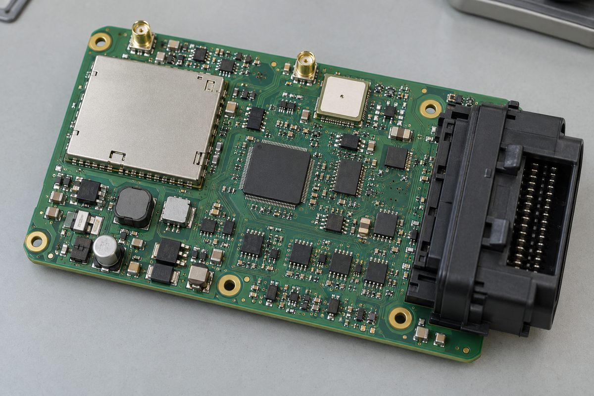
Package Terminal Format Mounting PCB / Routing Impact Assembly and Inspection Typical Trade-Off
DIP Two rows of pins Through-hole Drilled holes and wider body; simple routing Visible joints; hand, wave, or selective soldering may be used Easy to inspect and service, but consumes board area
SOP / SOIC Gull-wing leads on two sides Surface mount Moderate density with accessible fan-out Joints are generally visible to AOI Practical assembly, but lower density than bottom-terminated packages
QFP Gull-wing leads on four sides Surface mount Moderate-to-high perimeter pin count; outward fan-out Lead coplanarity and bridge control matter; joints remain visible Inspectable, but fine leads can bend and demand precise printing
QFN Bottom lands, often with exposed pad Surface mount Compact footprint and short connections; thermal-pad design may dominate Limited side fillet; X-ray may support hidden-joint evaluation Good density and, with a designed exposed pad, an effective thermal path; process visibility is lower
LGA Flat underside lands Surface mount Dense bottom contacts; escape strategy depends on land map Hidden joints require process control; X-ray and electrical tests provide complementary evidence Low profile, but solder volume, coplanarity, and warpage need control
BGA Underside solder-ball grid Surface mount High I/O density; may require fine vias, via-in-pad, or more layers Joints are hidden; X-ray and electrical tests become important High I/O count per board area, but routing and rework are more demanding
CSP Package-dependent lands or balls within chip-scale size limits Surface mount Very small footprint; fan-out depends on whether the CSP uses lands, balls, or a wafer-level layout Printing, placement, warpage, moisture, and inspection need close control Chip-scale size, but construction-specific manufacturing limits must be checked

DIP and SOP are easier to probe, route, and rework. QFP accommodates more connections while keeping the leads visible. QFN and LGA save space and shorten connections, but their critical joints sit beneath the body. BGA and CSP raise connection density further, making footprint control, fabrication, reflow, X-ray inspection, and repair planning more demanding.

How Can You Identify IC Package Types by Body, Leads, Pitch, and Markings?

Identify a package by combining its body geometry, terminal form, terminal count, pitch, dimensions, and manufacturer marking. Visual appearance alone is unreliable because different families can share similar outlines, and one family may contain several pitches or body sizes.

  1. Read the complete device marking. Record the top code, logo, orientation mark, and any secondary lot or date information without assuming the shortest code is the orderable part number.
  2. Inspect the terminal structure. Look for through-hole pins, two-sided gull-wing leads, four-sided leads, bottom lands, or a ball grid. Use magnification when the body hides terminal edges.
  3. Measure the body and lead span. Check length, width, height, lead-to-lead span, terminal width, and exposed-pad dimensions with suitable calibrated equipment.
  4. Determine pitch correctly. Measure center-to-center terminal spacing across multiple terminals when possible, then divide by the number of intervals to reduce single-point error.
  5. Locate the manufacturer package drawing. Match the measured features, pin count, orientation scheme, and dimensional tolerances to the exact orderable code.
  6. Verify the footprint source. Confirm that the CAD library item was built from the same drawing revision and not from a visually similar package.

If the underside is accessible, a bottom view can separate QFN or LGA lands from a BGA ball grid; X-ray can help when the joints are hidden. Body size alone is poor evidence. A mistaken identification can reverse pin numbering, omit an exposed pad, use the wrong pitch, or produce a plausible-looking footprint that will not solder reliably.

Engineer identifying IC package types by body leads pitch and orientation markings

Which IC Chip Package Types Suit Different PCB Assembly Requirements?

The best IC chip package type is the one that meets electrical, thermal, mechanical, inspection, repair, and production-volume requirements together. Selecting only for minimum board area can create a package that the available PCB stackup or assembly line cannot build consistently.

  • Prototypes and educational hardware: DIP, larger-pitch SOP, and accessible QFP packages simplify probing, manual rework, and visual inspection.
  • General industrial control: SOP, QFP, and appropriately sized QFN packages can balance density, cost, sourcing, and serviceability.
  • Compact portable products: QFN, LGA, BGA, and CSP reduce area, but need verified fine-pitch fabrication, printing, placement, reflow, and inspection capability.
  • High-I/O processors and FPGAs: BGA often supports the required connection count, although fan-out may force additional layers, smaller vias, or HDI construction.
  • Power devices: Packages with exposed pads or dedicated thermal connections can transfer heat into the PCB when copper, vias, interface conditions, and airflow are designed as one thermal path.
  • Repair-sensitive equipment: Visible-lead packages may reduce inspection and rework difficulty, even when they use more board area.

Geometry is only half of the selection. Check the full manufacturer part number, lifecycle status, authorized sources, moisture sensitivity, packing method, and any alternate-package plan. A functionally equivalent device in another package is not a drop-in replacement: its footprint, pin map, thermal path, firmware assumptions, and assembly route all need a fresh review.

How Do IC Package Types Affect PCB Footprints, Fan-Out, and Stackup Design?

IC package types determine pad geometry, routing exits, via strategy, reference-plane continuity, layer count, and fabrication difficulty. The design should begin with the exact package drawing and an approved land-pattern method, then be checked against the PCB fabricator’s real capabilities.

  1. Build or verify the footprint. Confirm terminal numbering, nominal and tolerance dimensions, toe/heel/side goals where applicable, exposed pads, solder-mask openings, paste layers, courtyard, polarity, and component height.
  2. Plan fan-out before routing the board. Two-sided and four-sided leaded packages usually escape outward. QFN and LGA may need short neck-down routes or local vias. BGA escape depends on ball pitch, depopulated channels, via pad size, anti-pad clearance, and layer allocation.
  3. Select vias with the fabricator. Through vias are economical when geometry permits. Fine-pitch arrays may require blind microvias or filled and capped via-in-pad. These processes must be defined in the fabrication data and quotation.
  4. Protect return paths. High-speed signals need continuous reference planes and nearby return transitions. Package escape should not create long stubs, plane splits, or uncontrolled neck-down sections.
  5. Design the thermal path. Exposed pads, copper spreading, thermal vias, internal planes, board thickness, interface materials, heat sinks, and airflow must be evaluated together.
  6. Freeze the stackup with real geometry. Impedance, drill aspect ratio, microvia depth, copper thickness, dielectric selection, and registration capability can change the feasible fan-out.

A generic library footprint can save drafting time, but it does not prove manufacturability. CAD checks may pass even when paste coverage, mask webs, via treatment, or the courtyard conflicts with the chosen process. Verify the source drawing, complete DFM review, and approve the controlled library item before release.

How Do IC Package Types Affect Stencil Design, Reflow Soldering, and Inspection?

Package geometry changes the solder-paste volume, aperture strategy, placement tolerance, thermal profile, and inspection method. Fine-pitch and bottom-terminated components generally provide less margin for printing variation and less direct visual access after reflow.

  1. Review pad and aperture geometry. Start from the approved footprint, then adjust aperture size, shape, segmentation, and local stencil treatment for the solder-paste process and component termination.

  2. Control exposed-pad paste. Large center pads are commonly divided into smaller apertures to manage deposited volume and outgassing. The appropriate coverage depends on package guidance, board design, paste, stencil, and process capability.
  3. Verify printing performance. Inspect paste deposits for release, alignment, bridging, insufficient volume, and contamination. Solder paste inspection can provide process feedback before components hide the deposits.
  4. Place within the real tolerance window. Nozzle selection, component pickup, vision recognition, board support, and placement force must suit the body and terminal structure.
  5. Develop the reflow profile. Use solder-paste guidance, component temperature limits, board thermal mass, package moisture controls, and measured board locations. Avoid copying a profile from a different assembly.
  6. Inspect by joint visibility. AOI can evaluate many gull-wing joints. QFN, LGA, BGA, and CSP connections may require X-ray, electrical test, boundary scan, or functional test because critical joints are hidden.
  7. Close the loop. Relate defects to paste, placement, reflow, footprint, board finish, component condition, and handling instead of changing one parameter without evidence.
X-ray inspection of hidden solder joints for bottom-terminated IC package types

Which IPC and JEDEC Standards Apply to IC Packages and PCB Land Patterns?

IPC documents mainly guide PCB land patterns, assembly processes, and acceptance, while JEDEC documents address semiconductor package outlines, terminology, handling, and reliability topics. The applicable revision and customer contract must be checked before a requirement is treated as mandatory.

Reference Primary Scope Engineering Use Important Boundary
IPC-7351 and IPC-7352 Surface-mount land-pattern principles and current design guidance Use IPC-7351 as a legacy framework and check IPC-7352 when establishing current land-pattern practice IPC lists IPC-7351 as no longer maintained; use the exact package drawing and the revision required by the customer contract
IPC-7093 and IPC-7095 Design and assembly guidance for bottom-termination components and BGAs Reviews package implementation, PCB design, assembly-process, inspection, and reliability considerations Use IPC-7093 for QFN/LGA-style bottom terminations and IPC-7095 for BGA applications; confirm the current revision
IPC-7525 Stencil-design guidance Supports aperture and stencil decisions for solder-paste printing Device guidance, paste behavior, board design, and demonstrated process capability still control the released stencil
J-STD-001 Soldered electrical and electronic assemblies Process and workmanship requirements under the agreed product class and contract It does not supply the component manufacturer’s package dimensions
IPC-A-610 Electronic-assembly acceptance Post-assembly acceptance criteria, including visual examples and product-class interpretation Hidden joints may need additional methods and customer-defined evidence
JEDEC JEP95 registered outlines Registered semiconductor-device package outlines Provides standardized outline references when adopted by the component supplier The component datasheet and orderable package drawing control the purchased part
J-STD-020 Moisture/reflow sensitivity classification for plastic surface-mount devices Supports component reflow qualification and classification review It is not a replacement for the assembly’s measured reflow profile
J-STD-033 Packaging and handling of moisture-sensitive nonhermetic solid-state surface-mount devices Controls exposure, storage, dry packing, and recovery actions IPC lists Revision D as no longer maintained; apply the contractual revision, component classification, and actual floor-life history

Record the component-drawing revision, land-pattern source, assembly class or agreed acceptance criteria, X-ray or void limits, moisture controls, and required test evidence in the release package. If the drawing, standard, and purchase specification disagree, resolve the conflict before production starts.

What Limitations, Assembly Defects, and Reliability Risks Affect Each Package Type?

Every package type exchanges one advantage for another, and its dominant risks follow the terminal geometry and assembly process. Visible leads improve inspectability but can bend. Hidden lands increase density but reduce direct inspection. Fine pitch saves area but narrows printing, placement, routing, and rework margins.

  • DIP: bent pins, incomplete hole fill, solder bridging, barrel damage during rework, and excessive board area.
  • SOP / SOIC: bridges, opens, lifted leads, insufficient solder, polarity errors, and lead coplanarity problems.
  • QFP: bent fine-pitch leads, bridging, opens, lead-to-pad misalignment, and handling damage.
  • QFN: insufficient edge-joint formation, center-pad voiding, floating from excess paste, opens, shorts, and thermal-path inconsistency.
  • LGA: hidden opens, uneven solder volume, warpage sensitivity, contamination, and limited rework visibility.
  • BGA: head-in-pillow where a ball and paste deposit do not fully join, non-wet opens, bridging, voiding, pad cratering, warpage-related defects, and difficult fault localization.
  • CSP: very narrow process margins, board-flex stress, underfill trade-offs, moisture/reflow sensitivity, and fatigue under thermal or mechanical cycling.

The operating environment can overturn an otherwise sensible package choice. Vibration, board bending, drops, thermal cycling, high junction temperature, contamination, and repeated rework stress different joints in different ways. There is no universally most reliable family; qualify the package together with the board, alloy, assembly process, enclosure, and actual load profile.

How Should Engineers Review IC Package Selection and Assembly Failures?

Review package selection before layout release, then investigate assembly failures by tracing the exact part, footprint, PCB data, process history, inspection evidence, and electrical symptom. Selection prevents avoidable incompatibilities; failure review isolates the mechanism after a defect appears.

  1. Define the selection requirements. Record I/O count, electrical speed, power dissipation, board-area limit, height limit, environment, inspection access, repair strategy, production volume, and approved sourcing constraints.
  2. Compare feasible package options. Check each candidate’s pin map, thermal path, fan-out demand, footprint availability, PCB stackup impact, assembly process, inspection coverage, lifecycle status, and total manufacturing risk before approval.
  3. Freeze the evidence. Record the exact part number, manufacturer, package code, lot information, board revision, BOM revision, placement data, paste, stencil revision, reflow profile, and inspection records.
  4. Compare source dimensions. Check the package drawing against the controlled footprint, including pin map, body size, lead span, pitch, terminal dimensions, exposed pad, solder mask, and paste layers.
  5. Check board manufacturability. Review pad registration, solder-mask web, via treatment, copper balance, local warpage risk, surface finish, fan-out, and stackup constraints.
  6. Reconstruct the assembly process. Examine paste printing, board support, placement offsets, component handling, moisture exposure, measured reflow temperatures, cooling, cleaning, and rework history.
  7. Use complementary inspection. Combine visual inspection, AOI, X-ray, electrical test, continuity checks, boundary scan, functional test, microscopy, cross-sectioning, or destructive dye-and-pry analysis only when each method fits the suspected failure.
  8. Separate symptom from cause. An intermittent signal may originate from a solder joint, via, trace, component, connector, firmware state, or test fixture. Confirm the physical failure mechanism before changing the design.
  9. Control the corrective action. Update the footprint, stencil, profile, handling rule, test limit, or supplier instruction through revision control, then verify the change on an appropriate build.

A useful review ends with marked package drawings, a footprint comparison, relevant X-ray or section images, test records, a confirmed failure mechanism, named corrective-action ownership, and a controlled release package. “Difficult to assemble” is not a finding; the records must show what failed, why it failed, and how the correction will be verified.

FAQs About IC Package Types

Q1: Why must the complete orderable part number be checked?

A1: A shared device name does not guarantee the same package, pin map, temperature grade, or packing option. Suffixes are manufacturer-specific and may identify body dimensions, terminal finish, reel quantity, orientation, or qualification grade. Match the complete code to the current datasheet, package drawing, approved BOM, and purchase order before releasing the footprint or substitute.

Q2: How should tape-and-reel orientation be confirmed?

A2: Confirm the supplier’s packing drawing, pin-one orientation, pocket direction, and reel feed direction. The component drawing alone may not define how the part arrives at the placement machine. Compare the packing specification with centroid rotation, feeder setup, assembly drawing, and first-article inspection. This prevents systematic rotation errors across an entire reel.

Q3: What is package coplanarity and why does it matter?

A3: Coplanarity is the variation in height among terminals that should contact the PCB during soldering. Excessive variation can leave one or more leads, lands, or balls above the paste deposit and create opens. Use the component specification for the allowable value, then consider PCB flatness, paste height, placement force, and reflow warpage before assigning the cause.

Q4: Should thermal vias be placed inside an exposed pad?

A4: Thermal vias can improve heat transfer, but their size, pitch, fill, and surface treatment must be controlled. Open vias may draw solder away from the joint or release trapped gas during reflow. Agree on via construction with the PCB fabricator and assembler, segment the paste pattern where appropriate, and verify the thermal design against the component supplier’s guidance.

Q5: Should fine-pitch package pads be solder-mask-defined?

A5: No single solder-mask strategy is correct for every fine-pitch package. Mask-defined and copper-defined pads change exposed copper geometry, mask registration sensitivity, solder behavior, and repair risk. Follow the component and land-pattern guidance, check the fabricator’s minimum mask web and registration capability, and review the complete pad array instead of applying one rule to every terminal.

Q6: How should package height and mechanical clearance be verified?

A6: Use the maximum package height and tolerance from the controlled drawing, not only the nominal 3D model. Check enclosure clearance, heat sinks, shields, connectors, test fixtures, and neighboring components. Include PCB thickness and warpage tolerances where they affect the assembly envelope. A mechanical interference review should be completed before the board and enclosure are released.

Q7: When should underfill be considered beneath a BGA or CSP?

A7: Underfill may help when drop, bending, vibration, or thermal-fatigue loads exceed the unsupported joint margin. It also changes reworkability, inspection, material compatibility, cure conditions, and stress distribution. Select it through product-level reliability analysis and qualification, not as an automatic repair for poor soldering. Confirm keep-outs and dispensing access before layout release.

Q8: How many times can an IC package be reworked safely?

A8: There is no universal safe number of rework cycles. The limit depends on component temperature exposure, moisture condition, pad integrity, laminate damage, solder alloy, warpage, cleaning, and the approved repair procedure. Record every heat cycle, inspect the site and surrounding parts, and stop when the component or PCB no longer meets the defined acceptance criteria.

Q9: Can any lead-free IC package use the same lead-free reflow profile?

A9: No; “lead-free” does not define one universal thermal limit or process window. Check the component’s declared reflow classification, package thickness, moisture sensitivity, terminal finish, and supplier limits. The assembly profile must also suit the solder paste and measured board temperatures. Verify both component exposure and solder-joint formation instead of relying on the alloy label alone.

Q10: What evidence should accompany X-ray inspection results?

A10: Retain the inspected location, image orientation, acceptance criteria, machine settings, and disposition. A single image without traceability may not show which component, board, or joint was evaluated. Link X-ray findings to visual inspection, electrical symptoms, process records, and destructive analysis when needed. State clearly which suspected defects the image can and cannot confirm.

Q11: How should an opened moisture-barrier bag be controlled?

A11: Record the opening time, ambient exposure, component moisture classification, and remaining floor life. Store, reseal, dry-pack, or bake parts only according to the applicable handling procedure and component limits. Do not reset exposure records by assumption. Maintain lot identity through kitting, return unused parts promptly, and keep humidity-indicator and desiccant evidence when required.

Q12: Can a downloaded CAD model be trusted for final mechanical release?

A12: Treat a downloaded model as a convenience file until its geometry and revision match the controlled package drawing. Check body dimensions, terminal position, seating plane, pin one, exposed pad, and maximum height. Library source names can be ambiguous, and models may omit tolerances. Approve the footprint and enclosure clearance from controlled dimensions, not appearance alone.

Need a quotation for PCB fabrication or assembly using DIP, QFP, QFN, LGA, BGA, or CSP components? Send your Gerber files, BOM, assembly drawings, and production requirements to sales@bestpcbs.com. EBest Circuit will review the package-related manufacturing requirements and prepare a quotation.

You may also like