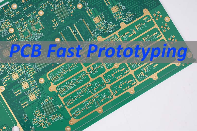
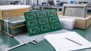
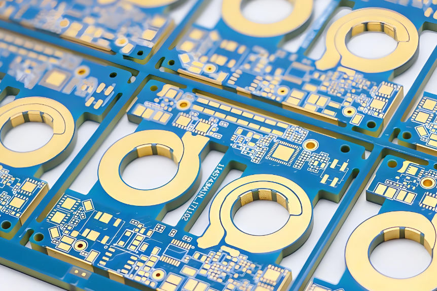
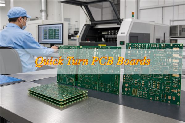
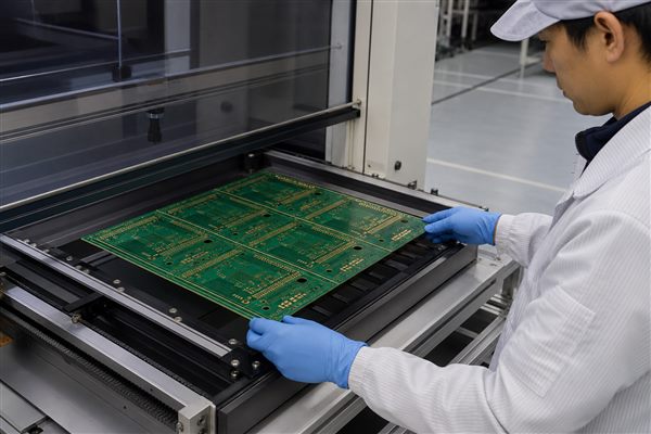
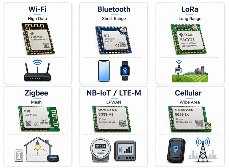
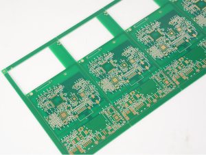
PCB fast prototyping helps engineers move a new board from design files to a real, testable sample before committing to larger production. It is useful when a project needs to verify fit, routing, material selection, surface finish, soldering quality, component sourcing, assembly process, and early functional performance.
EBest Circuit (Best Technology) supports PCB fast prototyping, DFM review, PCB fabrication, component sourcing, SMT assembly, testing coordination, and small-batch production. If your project is ready for prototype review, send your Gerber files, BOM, drawing, stackup notes, impedance requirements, or assembly files to sales@bestpcbs.com. Our engineering team can help better check the manufacturing path before production starts.
How PCB Fast Prototyping Helps Validate a New Board
PCB fast prototyping is not only about making a board quickly. The real value is helping engineers find practical problems early.
Whether the sample can move into small batch or mass production
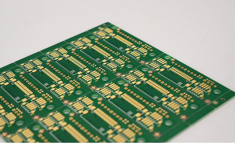
For a simple FR4 PCB, the prototype may mainly confirm mechanical size and soldering quality. For HDI, impedance, flexible PCB, rigid-flex PCB, metal core PCB, or PCBA projects, fast prototyping becomes much more important because the first build can reveal stackup, fabrication, assembly, and testing risks.
A good fast prototype should not be treated as a one-time sample. It should be built in a way that makes the next production step easier.
EBest Circuit PCB Fast Prototyping Lead Time
PCB fast prototyping lead time should be checked by board type, layer count, standard specification, and whether the project includes SMT assembly. A simple FR4 prototype can move much faster than an HDI board, ceramic PCB, rigid-flex PCB, or PCBA project with component sourcing.
For standard FR4 prototypes under 1 square meter, EBest Circuit can use the following lead time range as a practical reference:
FR4 Prototype
Normal Service
Fastest Service
1 layer
7 days
24 hours
2 layers
8 days
24 hours
4 layers
10 days
48 hours
6 layers
10 days
72 hours
8 layers
12 days
72 hours
10+ layers
To be confirmed
To be confirmed
This reference is based on standard FR4 prototype conditions, such as 0.4-1.6mm board thickness, H/H or 1oz copper, lead-free HASL, green solder mask, white silkscreen, minimum line width/space above 8 mil, minimum hole above 0.3mm, and minimum annular ring above 10 mil.
For other prototype types, the lead time needs separate review:
Prototype Type
Practical Lead Time Reference
1-layer MCPCB
Normal about 4 days; urgent service can be discussed
2-layer MCPCB
Longer than standard FR4 because of metal core processing
Rigid-flex PCB
About 2 weeks for common 4-layer projects; complex builds need review
Ceramic PCB
Usually longer because of substrate and process requirements
PCBA prototype
Depends on PCB, BOM sourcing, stencil, SMT, inspection, and packing
The fastest schedule is only realistic after the files are confirmed. If the board has special laminate, tight impedance, HDI microvias, heavy copper, black solder mask, fine-pitch SMT, special packing, or customer-approved production files, EBest Circuit will check these details before confirming the final delivery date.
For increasingly urgent projects, the best way is to send the Gerber files, BOM, drawings, stackup notes, and assembly files early, so the engineering and production teams can confirm whether the project fits fast service or needs a safer prototype schedule.
Fast Prototype PCB vs Standard PCB Production
A fast prototype PCB and standard PCB production have different goals.
Item
Fast Prototype PCB
Standard Production
Main goal
Verify the board quickly
Build repeatable batches
Quantity
Sample or small batch
Stable batch quantity
Review focus
DFM risks and urgent feasibility
Yield, cost, process control
Panelization
May be flexible
Usually optimized for production
Documentation
Basic to project-specific
More complete production records
Fast prototyping is best when engineers need quick feedback. Standard production is better when the design has already passed validation and the focus moves to cost, consistency, quality reports, and repeat delivery.
For many projects, the best path is:
Prototype first, review the result, adjust if needed, then move into small-batch or mass production.
PCB Fast Prototyping Capabilities at EBest Circuit
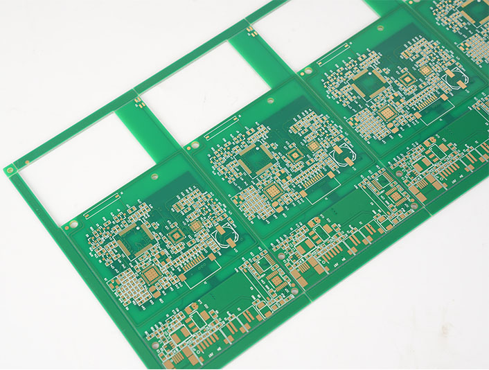
EBest Circuit supports PCB fast prototyping for standard FR4 boards, multilayer PCBs, HDI PCBs, metal core PCBs, ceramic PCBs, flexible PCBs, rigid-flex PCBs, and PCBA prototypes. For customers, the key is not only whether the board can be made quickly, but whether the prototype can be reviewed, built, assembled, tested, and prepared for the next production step.
For standard FR4 prototype projects, common fast-build conditions include:
Item
Reference Capability
Board thickness
0.4-1.6mm
Copper
H/H or 1oz
Surface finish
Lead-free HASL
Solder mask
Green
Silkscreen
White
Min line/space
>8 mil
Min hole
>0.3mm
Min annular ring
>10 mil
For projects beyond standard FR4, EBest Circuit can review more advanced requirements:
Area
Examples
Materials
High Tg FR4, halogen-free FR4, selected RF materials
These capabilities do not mean every project can use the same urgent schedule. A simple 2-layer FR4 sample may fit fast service, while an HDI board, heavy copper board, ceramic PCB, rigid-flex PCB, or full PCBA prototype needs engineering review before the lead time is confirmed.
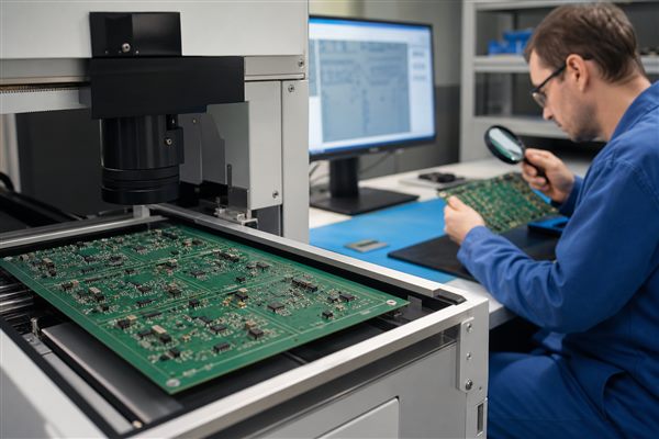
Before production, EBest Circuit early reviews the Gerber files, drill file, stackup, board thickness, copper thickness, surface finish, impedance notes, BOM, pick-and-place file, and packing requirements. This helps customers much more easily avoid a common problem: receiving a fast sample that cannot smoothly move into assembly or small-batch production.
Fast Turn PCB Prototype Process Step by Step
A fast turn PCB prototype needs a clear process. Speed is useful only when the project details are strictly controlled.
A typical EBest Circuit process includes:
File review Gerber files, drill files, drawings, stackup notes, and assembly files are checked.
DFM check Engineers review manufacturability risks such as spacing, holes, solder mask, copper, outline, and panelization.
Quotation and lead time confirmation The final price and schedule are confirmed based on board complexity and quantity.
Production data confirmation For special projects, production files or stackup details can be sent to the customer for confirmation before manufacturing.
PCB fabrication The board enters material preparation, imaging, etching, drilling, plating, solder mask, surface finish, profiling, and test.
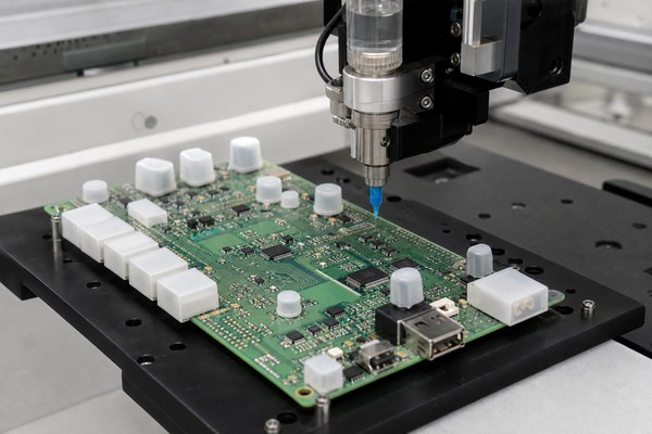
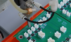
SMT assembly if required For PCBA prototypes, components are sourced or received, then assembled and inspected.
Final inspection and shipment Boards are checked, packed, and shipped according to project requirements.
This process keeps the prototype fast, but still controlled.
PCB Material and Surface Finish Options for Fast Prototyping
PCB material and surface finish should match the product use, not only the fastest delivery option.
Common fast prototype options include:
Option
Typical Use
FR4 Tg130
Standard electronics and general prototypes
FR4 Tg150 / Tg170
Higher heat or reliability requirements
1oz copper
Common signal and control boards
2oz copper
Higher current or thermal needs
HASL lead-free
Cost-sensitive prototypes
ENIG
Fine pitch, flat surface, better solderability
Green solder mask
Standard production choice
Black, white, blue, red mask
Appearance or product matching
For urgent projects, material availability can affect lead time. If a project uses special laminate, heavy copper, high Tg FR4, controlled impedance, HDI structure, FPC material, or special surface finish, the fastest realistic schedule should be confirmed after engineering review.
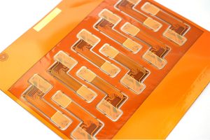
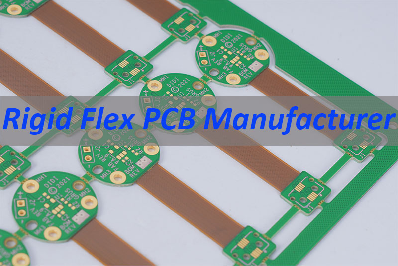
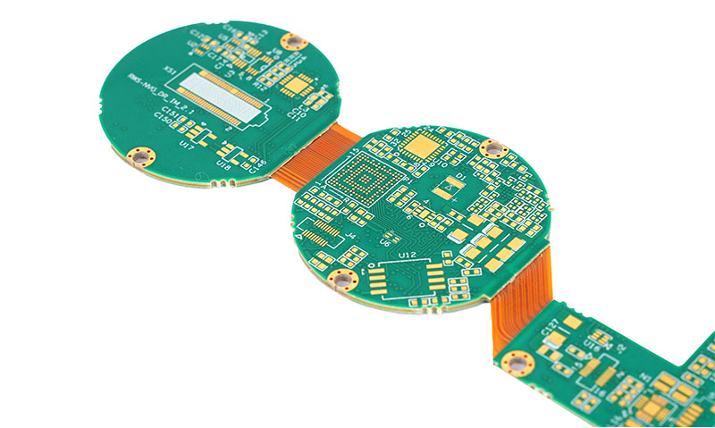
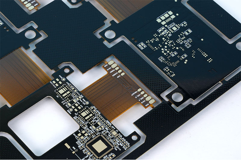
Fast Flexible PCB Prototyping and Rigid-Flex Prototype Support
Fast flexible PCB prototyping is useful for compact devices, wearable electronics, sensors, camera modules, connectors, medical electronics, and products with limited internal space.
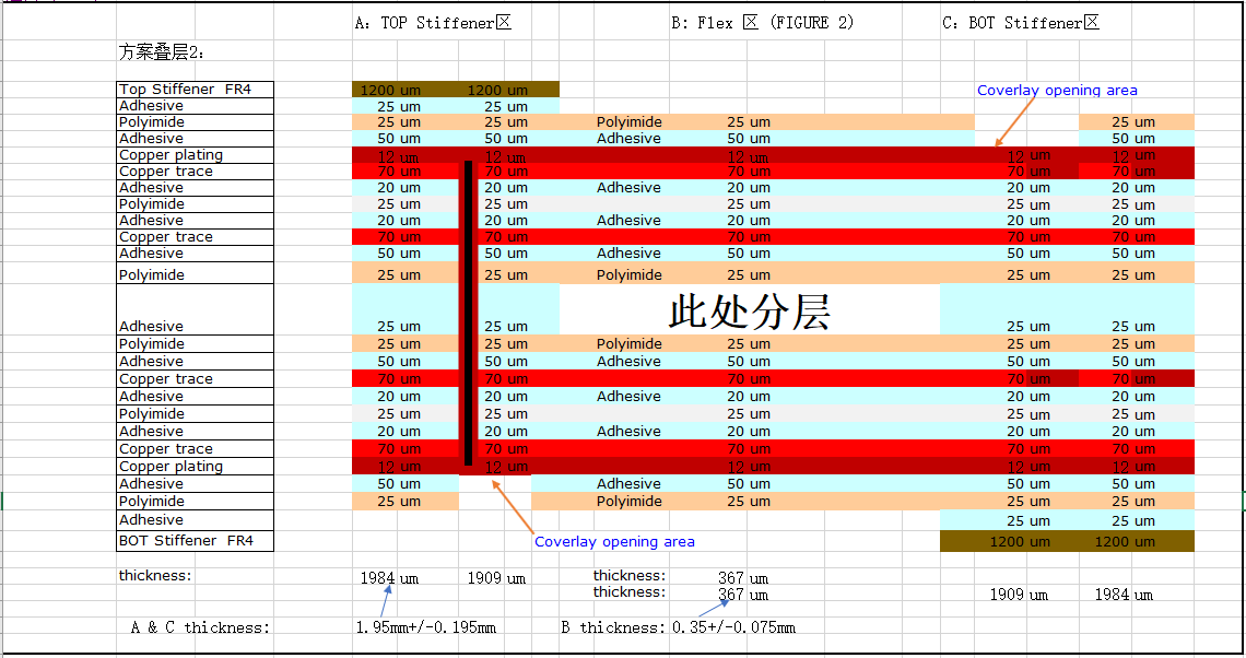
Flexible and rigid-flex prototypes require more attention than standard rigid PCBs because the board may include:
Area
What Needs Review
Flexible area
Bend direction and dynamic or static use
Coverlay
Opening size and adhesive control
Stiffener
Connector or soldering support
Material
PI, copper type, thickness
Rigid-flex transition
Stress and manufacturing reliability
Assembly
SMT support and handling protection
EBest Circuit can support flexible PCB and rigid-flex PCB prototype review based on customer-provided design files and product requirements. For these boards, fast delivery must be balanced with material selection, process reliability, and production yield.
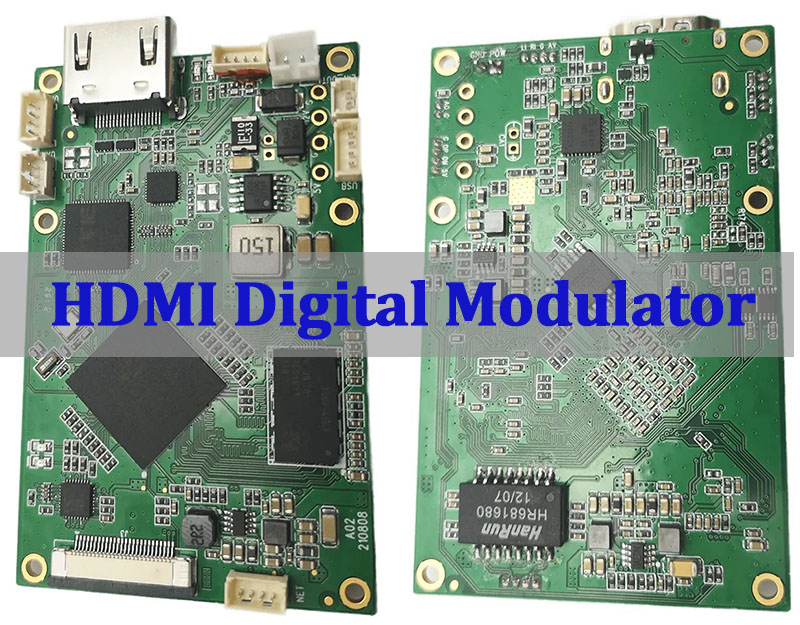
PCB Fast Prototyping Case Study
One fast prototype project involved a 4-layer FR4 PCB that needed both bare PCB fabrication and SMT assembly support.
Project background
The customer needed a prototype build for product validation before moving toward a more stable production plan. The project was not only a bare PCB order because EBest Circuit also handled component purchasing and SMT assembly.
Key board requirements
Item
Requirement
Board type
4-layer FR4 PCB
Material
FR4 Tg130
Finished thickness
1.6mm ±10%
Copper thickness
1oz / 1oz / 1oz / 1oz
Solder mask
Black
Silkscreen
White
Surface finish
Lead-free HASL
Panelization
Factory panelization allowed
Components
Purchased by EBest Circuit
Delivery
Single-unit delivery after SMT
Main project focus
This prototype had three practical concerns.
First, the board needed a stable 4-layer FR4 manufacturing path. The engineering team checked the thickness, copper structure, solder mask, surface finish, and panelization method before production.
Second, the project required SMT support. Since all components were purchased by EBest Circuit, BOM review and sourcing coordination were part of the prototype schedule. This helped the customer avoid managing PCB fabrication and component purchasing separately.
Third, the customer requested single-unit delivery after SMT. That meant packing and handling needed to match the assembled board condition, not only the bare PCB condition.
For the customer, the value was not just a fast prototype PCB. The value was a complete prototype path: DFM review, PCB fabrication, component sourcing, SMT assembly, inspection, and delivery in one workflow.
Why Choose EBest Circuit for PCB Fast Prototyping?
EBest Circuit is suitable for customers who need more than a simple online prototype order.
Our support includes:
EBest Circuit Support
Customer Value
DFM pre-review
Find risks before production
Engineering support
Review PCB and PCBA manufacturing details
PCB + PCBA factory
Reduce handoff between suppliers
Component sourcing
Support approved BOM purchasing
SMT assembly
Build functional prototype boards
Prototype and small batch
Support R&D validation and early production
Quality certifications
ISO9001, ISO13485, IATF16949, AS9100D
Digital traceability
Track material, batch, cycle, and production status
For engineers, the best PCB fast prototyping supplier is not always the one that promises the shortest time. It is the one that can tell which parts of the project are simple, which parts need engineering review, and which risks should be solved before the board moves into production.
EBest Circuit supports prototype-to-production projects for customers who need custom PCB fabrication, component sourcing, PCBA assembly, and practical manufacturing support.
PCB Fast Prototyping FAQs
1. What is the difference between PCB fast prototyping and normal PCB prototyping? PCB fast prototyping focuses on shorter lead time for engineering validation. Normal PCB prototyping may follow a standard schedule, especially when the board has special material, HDI, impedance, flexible PCB, or assembly requirements.
2. Can fast PCB prototyping include SMT assembly? Yes. A fast PCB prototype can include SMT assembly if the BOM, placement file, Gerber files, and assembly notes are complete. The lead time must include component sourcing or component receiving, stencil preparation, SMT, inspection, and packing.
3. Is lead-free HASL suitable for fast prototype PCB projects? Lead-free HASL can be suitable for many standard FR4 prototype boards. If the board has fine-pitch components, BGA, or very flat pad requirements, ENIG may be a better option.
4. Can EBest Circuit support fast flexible PCB prototyping? Yes. EBest Circuit supports flexible PCB and rigid-flex PCB prototype projects. The lead time depends on material, stackup, coverlay, stiffener, surface finish, and inspection requirements.
5. What files should I send for PCB fast prototyping? Please send Gerber files, drill files, board drawing, stackup notes, BOM, pick-and-place file, assembly drawing, impedance notes, and any special requirements such as thickness tolerance, surface finish, panelization, testing, or packing.
In short, a fast prototype should help you move forward, not create more uncertainty. If you are preparing a new PCB or PCBA project, send your Gerber files, BOM, drawings, stackup notes, impedance requirements, or assembly files to sales@bestpcbs.com. EBest Circuit will help review the manufacturing path and support your project from prototype validation to scalable production.
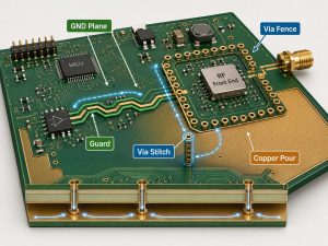
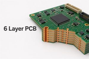
A capable 6 layer PCB manufacturer should do more than laminate six copper layers. The supplier must translate electrical requirements into a manufacturable stackup, control impedance, protect registration through lamination, inspect plated features, and keep fabrication data aligned with assembly requirements.
EBest Circuit supports PCB design, prototyping, mass production, component sourcing, and assembly from one project file set. Submit the required stackup, impedance targets, Gerber or ODB++ data, drill files, quantity, and acceptance criteria before production begins. This helps produce an accurate quotation and prevents late changes to trace geometry or dielectric spacing.
What Is a 6 Layer PCB and When Should You Use It?
A 6 layer PCB has six conductive copper layers. They are separated by dielectric material. This construction is often selected when a four-layer board lacks routing space, reference planes, power distribution, or electromagnetic control, while an eight-layer construction would add unnecessary complexity.
Common assignments use the outer layers for components and signals, two inner layers as continuous reference planes, and the remaining inner layers for signals or power distribution. The exact arrangement depends on signal speed, return-current paths, component density, power rails, board thickness, and the fabricator’s available materials. When these constraints exceed what a four-layer stack can manage, moving to six layers provides four practical advantages:
High-density routing: More internal routing capacity helps escape fine-pitch BGAs without forcing every connection onto the outer layers.
Signal integrity: Closely coupled reference planes provide controlled return paths for high-speed and impedance-sensitive signals.
Power distribution: Dedicated or shared plane layers can reduce loop area and organize multiple supply rails.
EMI control: A deliberate layer order helps contain fields and reduces discontinuities caused by split or missing references.
Why Choose a 6 Layer PCB Instead of a 4 Layer or 8 Layer PCB?
Use six layers when four are insufficient and eight add no value. Layer count should follow routing, reference-plane, electrical, and layout constraints rather than a fixed rule.
Decision Point
4 Layer
6 Layer
8 Layer
Routing density
Moderate
High
Very high
Reference-plane options
Usually two internal planes
More flexible plane and signal allocation
More dedicated planes and routing pairs
High-speed routing
Suitable for controlled layouts with limited density
Good balance of routing space and return paths
Useful for dense buses, many rails, or stronger field containment
Manufacturing burden
Lower
Moderate
Higher material and process content
A six-layer construction is not automatically cheaper than every eight-layer option. Standardized panel constructions, material utilization, via structure, copper weight, and factory loading can change the comparison. Request both stackup feasibility and a production quotation when the design can work on either layer count.
What Manufacturing Capabilities Should a 6 Layer PCB Manufacturer Provide?
A 6 layer PCB manufacturer must reproduce the approved stackup. Check the following six capabilities before releasing files or placing an order:
Stackup engineering: Confirm cores, prepregs, finished thickness, copper distribution, resin needs, and impedance structures before artwork release.
Registration control: Manage inner-layer alignment through tooling, imaging compensation, layup, lamination, and drilling.
Hole reliability: Review finished hole size, drill diameter, copper thickness, aspect ratio, annular ring, and any blind or buried via sequence.
Impedance verification: Calculate trace geometry from the production stackup and test representative coupons when specified.
Electrical testing: Verify opens and shorts against the released netlist or approved manufacturing data.
Documented inspection: Match inspection records and acceptance criteria to the product class and purchase order.
EBest Circuit offers FR-4, high-Tg, heavy-copper, HDI, high-speed, flexible, rigid-flex, and impedance-control products. Final limits must still be checked against the specific design through the verified PCB manufacturing capability and an engineering review.
What Materials, Copper Weights and Board Thicknesses Are Available?
Materials, copper weight, and thickness form one stackup system. Before quoting, the 6 layer PCB manufacturer should confirm how these choices affect impedance, drilling, copper balance, thermal performance, and lamination.
Variable
Common Starting Choice
Engineering Check
Base material
FR-4 or high-Tg FR-4
Confirm Tg, Td, CTE, Dk, Df, flammability requirement, and approved laminate family
Finished thickness
1.0, 1.2, 1.6, or 2.0 mm may be requested
Confirm tolerance, connector fit, stiffness, impedance, and available core/prepreg construction
Copper weight
1 oz is a common baseline
Separate starting copper from finished copper and review etching and hole-wall requirements
Surface finish
HASL, ENIG, OSP, immersion tin, or other qualified finish
Match shelf life, assembly process, pitch, bonding, contact use, and compliance needs
Heavy copper requires wider spacing, suitable resin flow, and careful copper balance. High-speed materials require the actual laminate data used for impedance calculations. The final 6 layer PCB thickness must be checked against connector fit, stiffness, drilling, copper weight, and the available dielectric construction.
How Should a 6 Layer PCB Stackup Be Designed?
A good stackup uses continuous planes and symmetric construction. Critical signals should remain next to uninterrupted reference planes. Release final trace widths and dielectric thicknesses only after the 6 layer PCB manufacturer confirms its production materials.
The following balanced structure is a practical starting point for dense digital and mixed-signal designs. It gives both outer signal layers a nearby ground reference and reserves the two center layers for additional routing or power distribution.
Layer
Typical Assignment
Reference and Design Purpose
L1 — Top
Components and critical signals
Route short high-speed connections over the solid L2 ground plane
L2
Solid ground plane
Provides the primary return path and impedance reference for L1 and suitable L3 traces
L3
Internal signals or power pours
Use L2 as the reference for controlled signals; keep power regions clear of critical return paths
L4
Internal signals or power pours
Use L5 as the reference for controlled signals; coordinate spacing from L3 to limit broadside coupling
L5
Solid ground plane
Provides the primary return path and impedance reference for L6 and suitable L4 traces
L6 — Bottom
Components and secondary signals
Route referenced signals over L5 and keep return paths continuous through layer changes
This arrangement is not universal. Before routing, confirm these four points with the manufacturer:
Reference continuity: Route critical nets over an uninterrupted ground reference and provide return transitions when changing layers.
Layer symmetry: Balance dielectric and copper construction around the center to reduce bow and twist risk.
Center-layer coupling: Set the L3-to-L4 spacing and routing directions to control broadside crosstalk.
Production construction: Size controlled traces from the manufacturer’s released cores, prepregs, copper thicknesses, and impedance model.
What Design Files and DFM Checks Are Required Before 6 Layer PCB Fabrication?
Send the 6 layer PCB manufacturer one consistent data set. It must define geometry, drilling, stackup, materials, impedance, finish, profile, and acceptance requirements. Assembly orders also need component and placement data.
Board image data: Supply Gerber X2 or ODB++ with a clear layer order and polarity.
Drill data: Include plated and non-plated holes, slots, countersinks, and controlled-depth features where applicable.
Fabrication drawing: State dimensions, tolerances, thickness, material, copper, finish, edge details, and special notes.
Impedance table: Identify net class, target, tolerance, layer, reference, width, and differential spacing.
Assembly package: Add BOM, centroid data, assembly drawings, approved substitutions, programming, and test instructions.
DFM should check annular rings, solder-mask clearances, copper-to-edge distance, drill-to-copper clearance, aspect ratio, via structures, copper balance, panelization, fiducials, tooling, and conflicts between drawings and data. Engineering questions should be closed in one approved revision set before the production clock starts.
How Does the 6 Layer PCB Manufacturing Process Work?
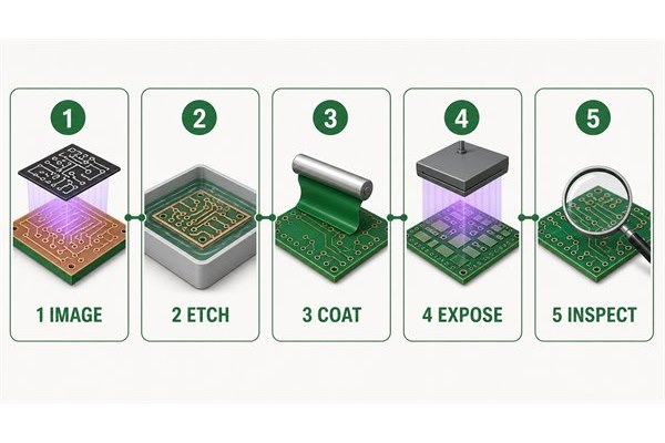
A 6 layer PCB manufacturer follows a controlled multilayer process. Production runs from data preparation and inner-layer imaging through lamination, hole metallization, outer-layer formation, finishing, and final testing. The following steps show what must be controlled before each operation advances.
Step 1 — CAM and DFM preparation: Engineers compare Gerber or ODB++ data, drill files, the fabrication drawing, stackup, impedance requirements, and panel dimensions. CAM tools create the production panel, drill programs, imaging data, layer-scaling allowances, and test coupons after file conflicts are resolved.
Step 2 — Inner-layer material preparation: Copper-clad cores are cut to panel size and cleaned so dry-film photoresist can bond uniformly. Material identity, copper weight, core thickness, surface condition, and orientation must match the approved stackup.
Step 3 — Inner-layer imaging: The circuitry for the internal copper layers is transferred to the resist by laser direct imaging or another qualified exposure method. Developing removes the selected resist areas and leaves the copper pattern required for etching.
Step 4 — Inner-layer etching and resist stripping: Unprotected copper is etched away to form the internal signal and plane patterns. The remaining resist is stripped, and conductor width, spacing, pad geometry, and unwanted residual copper are checked.
Step 5 — Inner-layer AOI and registration review: Automated optical inspection compares each etched inner layer with the approved CAM image to find opens, shorts, nicks, spacing defects, or missing features. Registration targets are also checked because these circuits will become inaccessible after lamination.
Step 6 — Bond treatment and six-layer layup: The inner copper surfaces receive a qualified bonding treatment, then cores, prepregs, and outer copper foils are stacked in the approved L1-to-L6 order. Tooling pins or another registration system align the layers, while prepreg type and resin content support dielectric thickness and copper filling.
Step 7 — Multilayer lamination: The six-layer book is pressed under a controlled temperature, pressure, vacuum, and time cycle. The prepreg resin flows, fills the copper topography, cures, and bonds the layers into one panel; the cycle must control thickness, voiding, registration, bow, and twist.
Step 8 — X-ray registration and drilling: After lamination, X-ray targets or approved tooling references locate the buried inner-layer features before drilling. Mechanical or laser drilling produces plated holes, non-plated holes, slots, and any controlled-depth features according to the drill program.
Step 9 — Desmear and hole-wall preparation: Drilling can leave resin smear over exposed inner-layer copper, so the holes are cleaned and micro-etched before metallization. This operation exposes sound copper and conditions the dielectric wall for a continuous conductive deposit.
Step 10 — Electroless copper and panel plating: A thin electroless copper layer makes the hole walls conductive, followed by electrolytic copper plating to build the required hole-wall and surface copper. Plating distribution and copper thickness are controlled because insufficient or uneven deposition can weaken plated-through holes.
Step 11 — Outer-layer imaging, pattern plating, and etching: The L1 and L6 circuit images are applied to the plated panel. Copper is built where required, an etch resist is added, unwanted outer copper is removed, and AOI checks the completed outer conductors against the CAM data.
Step 12 — Solder mask, legend, and surface finish: Solder mask is applied, imaged, developed, and cured while pad openings and mask dams are inspected. The specified finish is then applied to exposed copper, followed by legend printing when required; finish choice and thickness must match the assembly and product requirements.
Step 13 — Profiling, electrical test, and final release: Routing, scoring, or another approved method forms the final board outline and any internal cutouts. The finished boards undergo netlist electrical testing, dimensional and visual inspection, and any specified impedance, microsection, cleanliness, or documentation checks before packing and release.
What Specialized 6 Layer PCB Types Can We Manufacture?
Specialized six-layer boards require a matching process route. Six-layer construction can support rigid, heavy-copper, HDI, high-speed, flexible, and rigid-flex products. These options are not interchangeable add-ons.
Heavy copper: Suits higher-current and thermal demands but changes spacing, etching, resin filling, and finished-thickness planning.
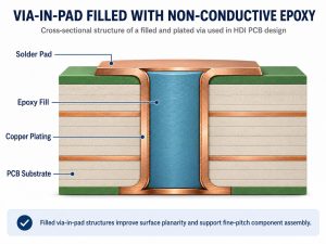
HDI: Uses microvias, sequential lamination, finer geometry, or via-in-pad structures when BGA escape density requires them.
High-speed and RF: Requires laminate control, loss planning, reference continuity, and production impedance correlation.
Flexible and rigid-flex: Requires bend-zone rules, coverlay, stiffeners, flex material control, and transition design. Review the verified flex PCB manufacturer requirements before release.
Send the complete mechanical and electrical requirements for feasibility review. A six-layer rigid-flex board, a six-layer HDI board, and a heavy-copper six-layer board follow different material and process controls even though the layer count is the same.
What 6 Layer PCB Manufacturing and Assembly Services Can We Provide?
Manufacturing and assembly stay coordinated from prototype to volume. Customers can place bare-board fabrication, component sourcing, and assembly under one controlled project revision.
Manufacturing starts with the approved board data and ends with inspected bare boards ready for assembly. The production scope should define the following requirements:
Stackup and material control: Build the six-layer construction from the approved core, prepreg, laminate grade, copper weight, finished thickness, and surface-finish requirements.
Impedance-controlled fabrication: Review controlled nets, target impedance, tolerance, reference layers, trace geometry, and the production stackup before releasing the board.
Drilling and plating: Manufacture through holes and any specified blind or buried vias according to finished-hole size, aspect ratio, annular-ring, and copper-plating requirements.
Bare-board inspection: Apply the agreed electrical test and dimensional inspection requirements before boards move to assembly or shipment.
Prototype and volume supply: Support initial board quantities and later mass production while keeping the approved fabrication revision under change control.
Assembly service adds parts procurement and component installation to the manufactured board. The order review should separate standard assembly work from project-specific operations:
Component sourcing: Purchase parts against the approved BOM and identify manufacturer part numbers, approved alternatives, do-not-substitute items, and customer-supplied components.
Assembly preparation: Check the BOM, pick-and-place file, assembly drawing, reference designators, polarity, package data, keep-out areas, and component-height restrictions for consistency.
Prototype assembly: Use the first build to confirm component fit, placement data, assembly notes, test access, and any programming requirements before volume release.
Volume assembly: Freeze the approved PCB revision, BOM, placement files, and substitution rules after sample approval to prevent mixed board or component revisions.
Project-specific operations: Programming, functional testing, conformal coating, special cleaning, traceability records, and detailed inspection reports require feasibility and acceptance-criteria confirmation during quotation.
To price manufacturing and assembly together, submit one complete and revision-matched data package. This allows material, component, tooling, testing, and delivery requirements to be reviewed at the same time:
PCB production data: Gerber or ODB++, NC drill files, board drawing, stackup, impedance table, panel requirements, and finished-board specifications.
Component data: BOM with manufacturer part numbers, quantities, approved alternates, do-not-substitute parts, and a list of consigned components.
Assembly data: Pick-and-place file, assembly drawing, polarity and orientation notes, reference designators, and any keep-out or height restrictions.
Order quantities: Prototype quantity, expected production quantity, delivery schedule, and whether extra boards or components are allowed for process setup.
Acceptance requirements: Required inspection records, electrical or functional tests, programming files, test fixtures, packaging, cleaning, coating, and traceability needs.
How Is Quality Controlled During 6 Layer PCB Fabrication and Assembly?
Quality must be verified at each production gate. This prevents hidden inner-layer, plated-hole, electrical, or assembly defects from reaching final inspection. Each gate should have a defined requirement, inspection method, acceptance limit, and release record.
Final visual and dimensional inspection results against released artwork and drawings
Electrical and impedance verification
Opens, shorts, netlist continuity, and controlled-impedance structures
Electrical-test status and impedance coupon data when coupon testing is included in the order
Assembly release
Component identity, orientation, solder-joint condition, workmanship, programming, and functional requirements
Specify the required inspection or test record; AOI, X-ray, programming, and functional testing remain order-dependent
Final shipment release
Board dimensions, quantity, revision, packaging, labeling, documentation, and nonconformance closure
Final inspection record, certificate of conformance, test report, or traceability record when contractually required
EBest Circuit lists ISO 9001:2015, ISO 13485:2016, IATF 16949, AS9100D, UL, RoHS, and REACH among its quality and compliance credentials. For regulated or high-reliability work, request the current certificate, site scope, product applicability, revision, and required order records before approval.
What Factors Affect 6 Layer PCB Price and Lead Time?
The full process route determines price and lead time. Layer count alone is not enough. A quote becomes reliable when it is based on released data and a confirmed stackup.
Panel utilization: Board dimensions, rails, coupons, routing gaps, and quantity determine material yield.
Material system: High-Tg, low-loss, flex, rigid-flex, or uncommon laminate choices affect availability and processing.
Copper and geometry: Heavy copper, fine lines, tight spacing, small annular rings, and dense drilling increase process difficulty.
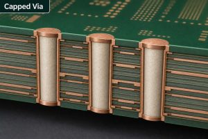
Via structure: Blind, buried, microvia, stacked, filled, or capped vias can add lamination and plating operations.
Testing scope: Impedance coupons, electrical test, microsection, ionic cleanliness, X-ray, programming, and functional test require time and resources.
Assembly supply chain: BOM availability, approved substitutions, component packaging, and fixture readiness often control the PCBA schedule.
Compare quotations using the same revision, quantity, material, copper, finish, test scope, quality documentation, shipping terms, and schedule start condition. A low headline price is not comparable if it excludes tooling, testing, controlled impedance, or assembly requirements.
Custom 6 Layer PCB Manufacturing and Assembly Case Study
A credible case study shows decisions and verifiable outputs. This representative industrial-control project explains what must be resolved before a custom six-layer board reaches production.
Project Background: The design needed more routing space than a four-layer board could provide. It also required continuous reference planes, multiple power rails, controlled-impedance signals, and an assembled prototype that would fit an existing enclosure.
Project Requirements: The release package contained Gerber and NC drill data, a preliminary stackup, impedance net classes, a BOM, pick-and-place data, assembly drawings, mechanical limits, programming requirements, and functional-test criteria. The main risks were inconsistent layer naming, incomplete impedance references, component substitutions, and uncontrolled changes between fabrication and assembly files.
Engineering Review: The board data was checked against the proposed layer order and drill pairs. Reference-plane continuity, BGA escape routing, copper distribution, panel requirements, dielectric availability, and manufacturable impedance geometry were reviewed together. BOM alternatives, polarity notes, package data, and test access were then resolved before release.
Manufacturing and Assembly Control: The approved stackup and artwork revision became the manufacturing baseline. The BOM, placement file, assembly drawing, and programming package were tied to the same revision so that a board change could not enter assembly without review.
Customer-Verifiable Output: The deliverable package can include the approved stackup, resolved engineering questions, released fabrication data, assembled samples, and electrical-test status. It can also include specified inspection records and a change log. These records let the customer compare the prototype and later production build against the same approved baseline.
Why Choose EBest Circuit as Your 6 Layer PCB Manufacturer in China?
One accountable source reduces handoff risk. Customers can coordinate design support, six-layer PCB production, component sourcing, and assembly through EBest Circuit, reducing the time and risk created by separate suppliers.
Fewer supplier handoffs: One project team can coordinate the stackup, bare-board data, BOM, placement files, and assembly requirements, reducing duplicated questions and conflicting revisions.
Lower design-release risk: Material availability, layer order, copper distribution, reference planes, drilling, impedance, and assembly data can be reviewed before production consumes material.
More predictable repeat orders: The approved manufacturing package and change history provide a controlled baseline for later builds instead of relying on undocumented production assumptions.
Simpler component coordination: Approved alternatives, customer-supplied parts, do-not-substitute items, and shortage decisions can be resolved within the same order as PCB production.
Quality evidence matched to your risk: Customers can specify electrical tests, impedance records, inspection reports, traceability, and certificates that their product or quality system actually requires.
Support from prototype to volume: PCB design, prototyping, mass production, component sourcing, and assembly services allow the same technical decisions to carry forward as quantities increase.
For a custom 6 layer PCB manufacturer quotation, send the released data package and identify the requirements that affect stackup, impedance, reliability, assembly, testing, quality records, and delivery.
FAQs About 6 Layer PCB Manufacturing
Q1: Can edge plating or castellated holes be added to a 6 layer PCB?
A1: Yes, when the board outline and plating requirements are designed for the selected feature. Define plated edges or castellations in the fabrication drawing and confirm minimum feature size, routing method, and finished-edge acceptance criteria.
Q2: Can press-fit connectors be used on a 6 layer PCB?
A2: Yes, but finished-hole geometry and plating must match the connector specification. Provide the connector drawing, compliant-pin range, hole tolerance, copper requirement, board thickness, and insertion-force constraints for review.
Q3: Should unused vias be tented, plugged, filled, or capped?
A3: Select the treatment from the via location and assembly risk. BGA escape vias, via-in-pad structures, exposed test vias, and holes near solderable pads may require different treatments to control solder loss, contamination, or surface flatness.
Q4: How should tooling holes and fiducials be specified for assembly?
A4: Define them at both board and panel level when the assembly process requires them. Their size, location, clearance, and relationship to breakaway rails should be coordinated with placement, inspection, and depaneling needs.
Q5: Can controlled-depth routing or cavities be used in a 6 layer PCB?
A5: These features are possible only after mechanical and stackup review. The drawing should define depth, tolerance, remaining dielectric or copper, corner radius, and the relationship to internal conductors.
Q6: What information is needed for selective conformal coating?
A6: Provide a coating drawing with coated and keep-out areas clearly marked. Identify connectors, test points, switches, heat sinks, grounding contacts, coating material, thickness requirement, masking method, and inspection criteria.
Q7: How should firmware and programming files be controlled?
A7: Treat firmware as a released production item with its own revision. Specify the device, file name, checksum or version, programming interface, security requirements, verification method, and labeling rule.
Q8: What packaging should be specified for assembled six-layer boards?
A8: Packaging should match moisture, ESD, mechanical, and cleanliness risks. Define ESD protection, moisture barrier requirements, desiccant, humidity indication, tray or reel orientation, cushioning, labels, and shipment quantity per package.
Q9: Can serial numbers, date codes, or lot codes be added?
A9: Yes, when the marking content, format, location, and data source are defined. Confirm whether markings are human-readable, machine-readable, permanent, linked to test records, or restricted by available board space.
Q10: How are approved component substitutions documented?
A10: Every substitute should be approved against defined electrical, mechanical, and lifecycle criteria. Record the alternate manufacturer part number, affected reference designators, approval authority, applicable quantity, and whether the change is temporary or permanent.
Conclusion
One approved production baseline reduces preventable variation. A reliable six-layer build keeps stackup, materials, impedance, drilling, plating, component data, inspection, and assembly under revision control. Coordinating these decisions with one manufacturing partner can reduce file conflicts, repeated engineering questions, component delays, and uncontrolled changes between prototype and volume production.
Send your Gerber/ODB++, NC drill files, stackup, BOM, and quantity, together with assembly drawings, programming files, test requirements, and required quality records, to sales@bestpcbs.com. EBest Circuit will review the manufacturing and assembly scope and prepare a project-specific quotation.
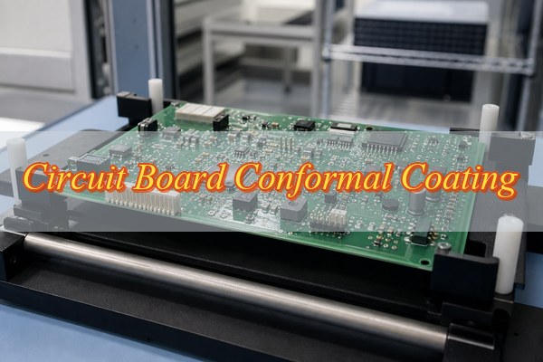
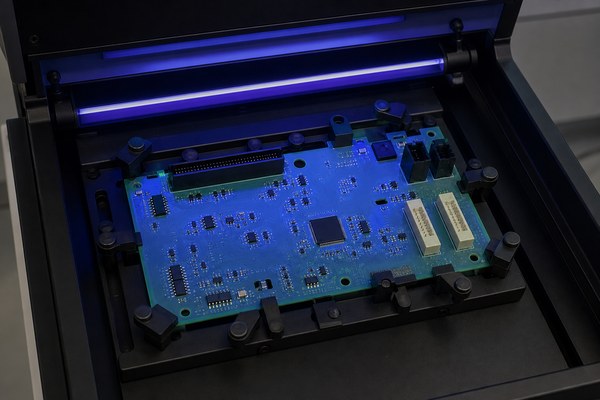
Circuit board conformal coating is a thin polymer film applied over an assembled printed circuit board to reduce damage from humidity, condensation, salt, dust, corrosive gases, and surface contamination. The right coating can improve insulation and field reliability without the weight and service restrictions of fully encapsulating the assembly.
Coating selection must match the operating environment, required service life, production method, inspection plan, and repair policy. A complete specification also preserves access to connectors, test points, adjustment devices, thermal interfaces, and other areas that must remain free of coating.
What Is Conformal Coating on Circuit Boards?
It is a thin, electrically insulating protective film. Unlike solder mask, which is applied during bare-board fabrication, conformal coating is normally applied after assembly and electrical testing. It follows the contours of components, solder joints, exposed conductors, and board surfaces while leaving specified keep-out areas uncoated.
A typical circuit board conformal coating is transparent and contains a fluorescent tracer for UV inspection. It is not automatically waterproof, hermetic, or suitable for immersion. Protection depends on the coating chemistry, film continuity, adhesion, thickness, edge coverage, cleanliness beneath the film, and compatibility with the operating environment.
Protection Layer
Process Stage
Primary Function
Rework Implication
Solder mask
During bare-board fabrication, before assembly
Cover selected copper and limit unwanted solder bridging
Permanent board finish; not removed for routine component repair
Conformal coating
After assembly, cleaning, and initial electrical test
Thin environmental barrier and surface insulation support
Local removal may be possible, depending on chemistry
How Does Conformal Coating Protect a Printed Circuit Board?
The film interrupts moisture and contamination paths. A continuous coating reduces direct contact between the assembly and conductive pollutants. It also increases surface insulation resistance, slows corrosion, and limits leakage or electrochemical migration when voltage bias, ionic contamination, and moisture would otherwise combine on the board surface.
The coating can also reduce the movement of fine dust, salt residue, and chemical mist toward exposed metal. Flexible chemistries may provide limited damping around small components. However, circuit board conformal coating cannot replace mechanical supports, strain relief, enclosure sealing, thermal design, surge protection, or proper ESD controls.
Moisture barrier: slows condensation and humidity from reaching conductors and solder joints.
Contamination control: reduces conductive paths formed by dust, salts, flux residue, and industrial deposits.
Corrosion delay: limits oxygen, water, and reactive species at vulnerable metal surfaces.
Insulation support: helps maintain surface resistance when coating coverage and cleanliness are controlled.
Mechanical restraint: offers limited support against light vibration, but does not replace structural fixation.
Which Circuit Boards Need Conformal Coating?
Boards exposed to predictable environmental stress benefit most. Coating is justified when the operating or storage environment presents condensation, high humidity, salt, dust, chemical vapor, fungus risk, or frequent temperature cycling. The decision should come from an environmental risk assessment rather than a blanket rule applied to every assembly.
Outdoor electronics: control boards inside vented or imperfectly sealed enclosures face condensation and airborne contaminants.
Industrial controls: factory air may contain conductive dust, oil mist, cleaning chemicals, or corrosive gases.
Transportation systems: automotive, rail, and marine electronics encounter humidity, salt, vibration, and temperature cycling.
HVAC and appliances: temperature changes can create condensation near power and control circuitry.
High-impedance circuits: sensor inputs and precision analog nodes are sensitive to small leakage currents.
Circuit board conformal coating may be unnecessary for a board installed in a controlled, sealed, dry indoor environment. It may also create more risk than value when unprotected switches, relays, sockets, optical surfaces, microphones, pressure sensors, or high-frequency tuning structures cannot be reliably masked.
What Are the Main Types of Conformal Coatings for Circuit Boards?
Five chemistry families cover most protection decisions. Circuit board conformal coating is commonly based on acrylic, polyurethane, silicone, epoxy, or parylene. These materials differ in chemical resistance, temperature behavior, cure method, film thickness, production equipment, and rework difficulty. UV-curable formulations form an additional production category and may use hybrid chemistry.
Type
Main Strength
Main Limitation
Rework
Acrylic
Fast drying and practical general protection
Lower solvent and high-temperature resistance
Usually easiest
Polyurethane
Strong moisture, abrasion, and chemical resistance
Acrylic conformal coating is often the practical starting point for general electronics because it dries quickly and supports local repair. It should not be selected by habit when the assembly faces fuels, aggressive solvents, sustained high temperature, or immersion.
What Is the Best Conformal Coating for PCB?
There is no universal best coating chemistry. The best conformal coating for PCB use must survive the defined environment and adhere to the cleaned assembly. It must also fit the production process and permit the required inspection and rework. A coating that is exceptionally resistant but impossible to repair may be the wrong business and engineering choice.
General indoor or light industrial use: evaluate acrylic where quick cure and repair access matter.
Chemical and abrasion exposure: evaluate polyurethane or epoxy after compatibility testing.
High temperature and thermal cycling: evaluate silicone with contamination controls.
Complex geometry and very uniform coverage: evaluate parylene when vacuum deposition and masking are justified.
High-volume production: evaluate UV-curable material with verified secondary cure in shadowed regions.
Circuit board conformal coating selection should compare the datasheet with operating temperature, humidity, chemicals, flammability requirements, dielectric performance, cure limitations, viscosity, application equipment, inspection method, and approved remover. Prototype boards should be coated and tested under representative stress before mass production.
What PCB Design, Cleaning and Masking Requirements Should Be Defined Before Coating?
Coating quality is largely decided before the coating is applied. Drawings should define coated zones, keep-out zones, allowable edge distance, thickness range, material designation, cure condition, inspection method, and acceptance criteria. Ambiguous notes such as “coat entire PCB” do not protect connectors, test access, adjustment points, or mating surfaces.
Coating boundaries: show coated sides, board-edge limits, permitted overspray, minimum clearance, and areas requiring complete coverage on a controlled drawing.
Functional keep-outs: identify connectors, sockets, contacts, switches, relays, test points, trimmers, sensors, microphones, vents, antennas, and optical surfaces.
Thermal and grounding interfaces: exclude heat-sink contact areas, chassis grounds, press-fit zones, and mating surfaces unless the design specifically permits coating.
Drain and shadow control: review tall components, narrow gaps, board edges, cavities, and underside regions for pooling, air entrapment, or missed coverage.
Component spacing: leave enough access around sensitive parts for masking, inspection, local removal, soldering, and later component replacement.
Pre-coating condition: define which assembly inspection, programming, functional test, and repair operations must be completed before coating begins.
Cleaning process: specify approved wash chemistry, concentration, time, temperature, rinse quality, mechanical action, and compatibility with components and labels.
Cleanliness acceptance: define visual residue limits and any required ionic contamination or surface-insulation-resistance evidence instead of relying on appearance alone.
Drying requirement: establish drying time, temperature, handling controls, and maximum delay before coating so moisture and new contamination are not trapped.
Material compatibility: qualify plastics, labels, inks, adhesives, thermal materials, elastomers, solder mask, and component coatings against the liquid material and cure cycle.
Masking materials: select removable tapes, dots, boots, plugs, or custom fixtures that resist solvent, application pressure, and cure without leaking or leaving residue.
Mask removal: define when masks are removed, how coating edges are cut if necessary, and how exposed keep-outs and lifted coating edges are inspected.
Applying circuit board conformal coating over flux, fingerprints, moisture, silicone contamination, or poorly dried wash residue traps the problem beneath the film. This can produce delamination, corrosion, leakage, bubbles, or inconsistent cure even when the coating material meets its specification.
The released process should also state who approves masking changes, how first-article coverage is verified, and which records travel with the production lot. These controls prevent an operator-level adjustment from silently changing protection or service access.
How to Conformal Coat a Circuit Board?
A controlled process starts with a tested and clean assembly. Brushing suits limited repair or low-volume work, spraying supports flexible coverage, dipping can coat both sides, and selective robotic dispensing provides repeatable boundaries in production. The method must match the coating viscosity, board geometry, keep-outs, and throughput.
Step 1 — Verify the assembly. Complete assembly inspection, programming, and required electrical testing before coating. Confirm that repairs are closed and the approved material, thinner, masks, drawing, and process revision match the work order.
Step 2 — Clean the board. Remove flux, oils, fingerprints, particles, and other specified residues with the validated chemistry and equipment. Protect moisture-sensitive or non-washable components and use the defined rinse quality.
Step 3 — Dry and verify cleanliness. Use the approved drying profile and confirm that liquid is not trapped beneath packages, shields, or connectors. Perform the required visual, ionic, or process-based cleanliness check before further handling.
Step 4 — Mask all keep-out areas. Protect contacts, test points, switches, vents, adjustment devices, antennas, optical surfaces, and thermal interfaces. Check every mask against the controlled drawing before application.
Step 5 — Prepare the coating. Verify the material lot, shelf life, storage history, temperature, mixing ratio, agitation, filtration, viscosity, and pot life. Use only approved thinner and do not return contaminated material to the original container.
Step 6 — Apply a controlled film. Set the nozzle, spray pattern, dispense path, brush load, withdrawal speed, board orientation, passes, and flash-off time for the chosen method. Apply thin, even passes and prevent pooling beneath components or along board edges.
Step 7 — Remove masks and cure. Remove masking at the validated stage so edges remain clean without tearing the film. Cure with the specified time, temperature, humidity, UV dose, or secondary reaction while controlling board support and spacing.
Step 8 — Inspect and release. Verify coverage, keep-outs, bubbles, dewetting, thickness, cure, adhesion, and any required electrical or functional result. Record material lot, process settings, inspection result, and nonconformance disposition before releasing the assembly.
How Thick Should Circuit Board Conformal Coating Be?
Use the material specification, not one universal thickness. Many liquid conformal coatings are specified in a dry-film range around 25–125 µm, while some silicone systems may permit thicker films and parylene is commonly much thinner. The approved drawing and coating datasheet must define the actual range.
Too little circuit board conformal coating leaves pinholes, thin edges, and weak barrier performance. Too much can crack, trap solvent, bridge keep-out boundaries, increase stress around components, extend cure time, and make repair difficult. Wet-film thickness must account for solids content because the film becomes thinner as solvent evaporates.
Measure thickness on a representative coupon, witness panel, or suitable flat board location using wet-film gauges, micrometers, optical methods, or noncontact instruments appropriate to the material. Do not assume that a programmed dispense volume proves dry-film thickness across tall components and shadowed areas.
How Is Conformal Coating Cured?
Cure chemistry determines the required production controls. Different products may cure through solvent evaporation, heat, moisture, UV energy, or chemical reaction. “Dry to touch” is not the same as fully cured. A surface may feel dry while solvent remains trapped or final chemical and electrical properties are still developing.
Cure Route
Control Point
Typical Risk
Ambient evaporation
Airflow, temperature, film thickness, flash time
Solvent entrapment or skinning
Thermal cure
Actual board temperature and dwell time
Component or material heat damage
Moisture cure
Humidity exposure and shadowed geometry
Slow cure in dry conditions
UV cure
Intensity, dose, distance, line speed, shadow cure
Uncured material beneath components
Two-part reaction
Mix ratio, mixing quality, pot life, temperature
Soft, brittle, or uneven cure
Circuit board conformal coating cure records should reflect the board’s real exposure, not only the oven or lamp setting. Where a UV material uses a secondary chemical cure, production must allow enough time for shielded areas beneath tall packages and connectors to complete that reaction.
What Are the Problems with Conformal Coating PCB?
Most defects trace to contamination, application, masking, or cure. Diagnose the mechanism before reworking the board. The same visible defect can have several causes, so a repair based only on appearance may repeat the failure.
Bubbles and pinholes: Entrained air, trapped solvent, porous residue, or fast surface drying can leave voids. Reduce agitation, control viscosity and film build, allow flash-off, and confirm that the board is clean and dry.
Dewetting and fisheyes: Oil, silicone, flux, mold release, or an incompatible surface can repel the liquid coating. Stop production, identify the contaminant, validate cleaning, and test surface compatibility before recoating.
Orange peel or rough texture: Incorrect viscosity, poor atomization, excessive spray distance, or rapid solvent loss can prevent leveling. Correct the material condition and spray settings, then verify the result on a representative board.
Pooling and excessive thickness: Heavy passes, low viscosity control, poor board orientation, or insufficient drainage can collect material around components. Use thinner passes, change orientation or path timing, and verify dry-film thickness.
Missed areas and thin edges: Component shadowing, unstable spray paths, poor wetting, or incorrect board orientation can leave exposed regions. Adjust the path, angle, speed, and number of passes, then confirm coverage under UV inspection.
Cracking: Excessive thickness, brittle chemistry, rapid cure, or thermal and mechanical strain can fracture the film. Remove unsound material, correct film build or cure, and qualify a more flexible coating when the assembly moves.
Whitening or haze: Moisture, solvent entrapment, incompatible cleaners, or cure conditions can cloud the coating. Verify drying, flash-off, environmental controls, and chemical compatibility before deciding whether the film must be removed.
Delamination: Moisture, residue, poor surface preparation, or incompatible materials can lift the coating from the board. Remove loose film, clean and dry the area, confirm adhesion, and recoat only after correcting the root cause.
Incomplete or tacky cure: Wrong mix ratio, expired material, insufficient heat or UV, excessive thickness, or shadowing can leave weak film. Quarantine the lot and verify material control, cure dose, profile, and secondary cure.
Coating on keep-outs: Mask leakage, movement, poor fixture design, or an unstable dispense boundary can contaminate contacts and service points. Remove the coating with an approved method, correct the mask or program, and reinspect every exclusion.
Circuit board conformal coating repair should begin only after the defect mechanism is understood. Simply applying another coat over contamination, uncured material, or delamination can hide the defect and make later removal harder. When leakage or corrosion is present, isolate whether it formed before coating, under the film, or after the film was damaged.
How Is Circuit Board Conformal Coating Inspected and Tested?
Inspection must verify coverage, exclusions, cure, and performance. Visible appearance alone cannot prove that the film meets its electrical or environmental purpose. A practical control plan combines visual or UV inspection, thickness verification, cure checks, adhesion assessment, cleanliness evidence, and application-specific reliability testing.
Visible and UV inspection: confirm coverage boundaries, bubbles, cracks, pooling, foreign matter, and clean keep-outs.
Thickness verification: measure the dry film using a method suitable for the coating and available geometry.
Cure assessment: use the supplier’s approved tack, hardness, solvent, weight, or process confirmation method.
Adhesion testing: validate adhesion on representative surfaces without damaging production hardware unnecessarily.
Electrical and environmental testing: apply insulation resistance, humidity, thermal cycling, salt, fungus, or chemical exposure when the application requires it.
IPC-CC-830 is commonly used to qualify conformal coating materials, while IPC-A-610 provides workmanship acceptance guidance for electronic assemblies. Project documents should state the required revision and acceptance class. A broader PCB board testing checklist should still cover electrical and functional verification before and after the coating process.
How to Remove Conformal Coating from Circuit Board?
Identify the coating before choosing a removal method. Solvent, thermal, mechanical, peeling, and micro-abrasive methods affect each chemistry differently. The wrong remover can craze connector housings, lift labels, swell elastomers, strip markings, soften adhesives, or damage the solder mask and laminate.
Step 1 — Identify the coating and substrate. Review production records, coating appearance, supplier data, and approved repair instructions. Confirm the likely chemistry before using heat, solvent, or abrasion because the wrong method can attack plastics, markings, adhesives, solder mask, or laminate.
Step 2 — Define and protect the repair area. Mark the minimum removal boundary and shield adjacent components, contacts, and uncoated surfaces. Provide suitable extraction and personal protection for the selected chemical or abrasive process.
Step 3 — Test the removal method. Apply the proposed circuit board conformal coating remover or mechanical technique to a noncritical sample, witness coupon, or hidden region. Verify that it softens the coating without swelling plastics, lifting labels, stripping markings, or damaging the board finish.
Step 4 — Remove only the required coating. Acrylic is often softened with a compatible solvent; some silicones can be cut and peeled; polyurethane may require stronger chemical or mechanical work. Cured epoxy and parylene commonly require specialized abrasion or other controlled processes. Work from the boundary inward and avoid scraping pads or driving debris beneath packages.
Step 5 — Clean, inspect, and complete the repair. Remove softened residue and particles with an approved cleaning process. Inspect exposed conductors, solder mask, component bodies, leads, and nearby coating edges before component replacement or soldering.
Step 6 — Restore the protective system. Mask the repaired area, apply a compatible replacement coating with overlap onto sound material, complete the specified cure, and reinspect coverage, adhesion, thickness, and keep-outs. Record the repaired location and material lot when traceability is required.
Conformal Coating vs Potting: Which PCB Protection Method Is Better?
Choose by exposure, serviceability, weight, and mechanical demand. Conformal coating provides a thin, light barrier and preserves inspection and local repair access. Potting fills a cavity with a much thicker resin, offering stronger mechanical restraint and environmental isolation but adding mass, thermal constraints, cure stress, and difficult rework.
Decision Factor
Conformal Coating
Potting
Protection structure
Thin film that follows the board and components
Thick resin that fills an enclosure or defined cavity
Moisture and contamination
Useful against humidity, condensation, dust, and chemical deposits when coverage is continuous
Stronger isolation when the resin, enclosure, interfaces, and cure are validated as a complete system
Mechanical support
Limited restraint; does not replace brackets, staking, or strain relief
Can immobilize components and cables, but cure shrinkage and expansion stress must be controlled
Weight and volume
Low material mass and minimal dimensional increase
Higher mass and volume; enclosure fill level must be controlled
Thermal behavior
Small thermal effect when thin, but thermal interfaces must remain clear
Can spread or trap heat depending on resin conductivity, voids, thickness, and enclosure design
Inspection and fault finding
Components and solder joints usually remain visible; UV tracer can show coverage
Internal features become difficult or impossible to inspect after cure
Repair and component replacement
Localized removal and recoating are often practical, depending on chemistry
Removal is usually slow, costly, or destructive to the assembly
Production controls
Cleaning, masking, viscosity, film thickness, coverage, and cure
Assemblies needing strong mechanical immobilization or deeper encapsulation
The full conformal coating vs potting decision should also consider heat transfer, trapped air, resin exotherm, component stress, enclosure geometry, fluid compatibility, repair policy, and end-of-life requirements. Hybrid protection may use circuit board conformal coating on the assembly and localized potting around vulnerable cables or high-stress regions.
What Affects Circuit Board Conformal Coating Cost?
Total cost is driven more by process complexity than liquid price. Material chemistry matters, but masking labor, board geometry, application method, cure time, inspection, cleaning, handling, repair rate, and production volume often dominate the finished cost. Parylene requires vacuum deposition, while selective coating requires programming and fixtures but can reduce repetitive masking.
Coated area and sides: larger boards and double-sided coverage consume more material and handling time.
Keep-out complexity: many connectors, switches, test points, and sensors increase masking and inspection labor.
Coating chemistry: material price, storage, pot life, cure, and removal requirements vary widely.
Production method: brushing, spray, dip, selective dispensing, and vapor deposition have different setup economics.
Quality evidence: thickness records, coupons, environmental testing, traceability, and special reports add controlled work.
Rework risk: defects discovered after cure may require costly local stripping, cleaning, and recoating.
A useful quotation package includes Gerber or ODB++ data, assembly drawings, BOM, board dimensions, quantities, and the coating material or performance specification. Also provide the coated sides, keep-out drawing, thickness range, cure requirement, inspection criteria, packaging needs, and required test records.
FAQs About Circuit Board Conformal Coating
Q1: Can conformal coating change RF or antenna performance?
A1: Yes, dielectric material near an RF structure can shift its behavior. Coating over antennas, resonators, impedance-sensitive traces, or tuning elements may change capacitance, resonance, loss, or matching. Define RF keep-outs during layout and validate the fully coated assembly rather than relying only on an uncoated prototype.
Q2: Can conformal coating be used on flexible circuits?
A2: It can, but bend zones require special qualification. A coating that performs well on rigid FR-4 may crack, wrinkle, or delaminate when a flex circuit is repeatedly bent. Review minimum bend radius, dynamic versus static use, coverlay compatibility, coating modulus, thickness, and flex-cycle testing before approval.
Q3: Does conformal coating prevent tin whiskers?
A3: It may reduce whisker-related bridging risk but cannot guarantee prevention. Performance depends on coating thickness, adhesion, flexibility, coverage, and the whisker’s growth force. Whisker risk should also be controlled through finish selection, material management, stress reduction, spacing, and application-specific reliability testing.
Q4: Does the UV tracer provide any environmental protection?
A4: The tracer is primarily an inspection aid, not the protective barrier. It fluoresces under the specified UV light so missed areas, boundaries, and coverage variation are easier to see. Its presence does not prove correct thickness, adhesion, cure, cleanliness, or resistance to the intended environment.
Q5: How should opened coating material be controlled?
A5: Track storage condition, opening date, shelf life, and usable life. Moisture exposure, solvent loss, repeated opening, contamination, poor mixing, or expired material can change viscosity and cure. Production should follow the supplier’s resealing, agitation, filtration, thinning, and disposal instructions and record the material lot used.
Q6: Is conformal coating suitable for electronics used in vacuum?
A6: Only a qualified low-outgassing system should be considered. Residual solvent, uncured material, absorbed moisture, and volatile additives can contaminate optics or nearby surfaces in vacuum. Material selection should use relevant outgassing data, complete cure verification, assembly-level testing, and the actual pressure and temperature profile.
Q7: Can conformal coating justify smaller creepage distances?
A7: Do not reduce spacing without the governing safety standard and qualification evidence. Some standards recognize coated assemblies under defined material, process, pollution, and test conditions, but an ordinary coating note is not sufficient. Voltage, environment, coating category, manufacturing control, aging, and certification requirements must all be reviewed.
Q8: How should a recoated repair area be documented?
A8: Record the location, reason, materials, process, and verification result. Useful traceability includes the board serial number, removed coating type, replacement material and lot, cleaning method, repair boundary, cure condition, inspection result, and operator or station. This record supports future failure analysis and repeat-order control.
Q9: Can a cured coated assembly be cleaned after field contamination?
A9: Yes, but the cleaning agent must be compatible with the cured film. Water, detergent, alcohol, or stronger solvents can soften, swell, haze, or undermine different coatings. Identify the contaminant, test a small area, avoid forcing liquid beneath components, dry the assembly completely, and reinspect the coating afterward.
Q10: What requires requalification after a coating change?
A10: Changes to chemistry, supplier, cure, thickness, or cleaning can affect reliability. Requalification scope may include adhesion, coverage, insulation resistance, thermal cycling, humidity, chemical exposure, flammability, RF behavior, and repair compatibility. The decision should follow formal change control and the product’s risk and regulatory requirements.
Conclusion
Reliable coating begins with a defined environment and process. Select circuit board conformal coating chemistry from actual moisture, chemical, temperature, repair, and production requirements; then control cleanliness, masking, thickness, cure, and inspection. The best result is not the thickest film, but a continuous and verified barrier that protects required areas without blocking service access.
For a useful quotation, submit the assembly files, BOM, quantities, operating environment, coating material or performance requirement, keep-out drawing, thickness range, cure requirement, and inspection or test records. This information allows the manufacturing plan to address risk before coating begins.
If you are planning a PCB or PCBA project, EBest Circuit can support PCB fabrication, component sourcing, PCB assembly, conformal coating requirements, inspection, testing, prototyping, and volume production. Send your Gerber or ODB++ files, BOM, quantities, coating specification, keep-out drawing, and test requirements to sales@bestpcbs.com for an engineering review and quotation.
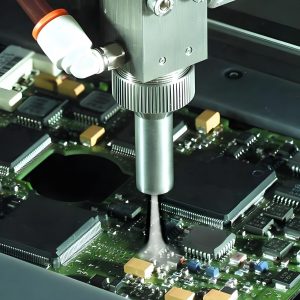
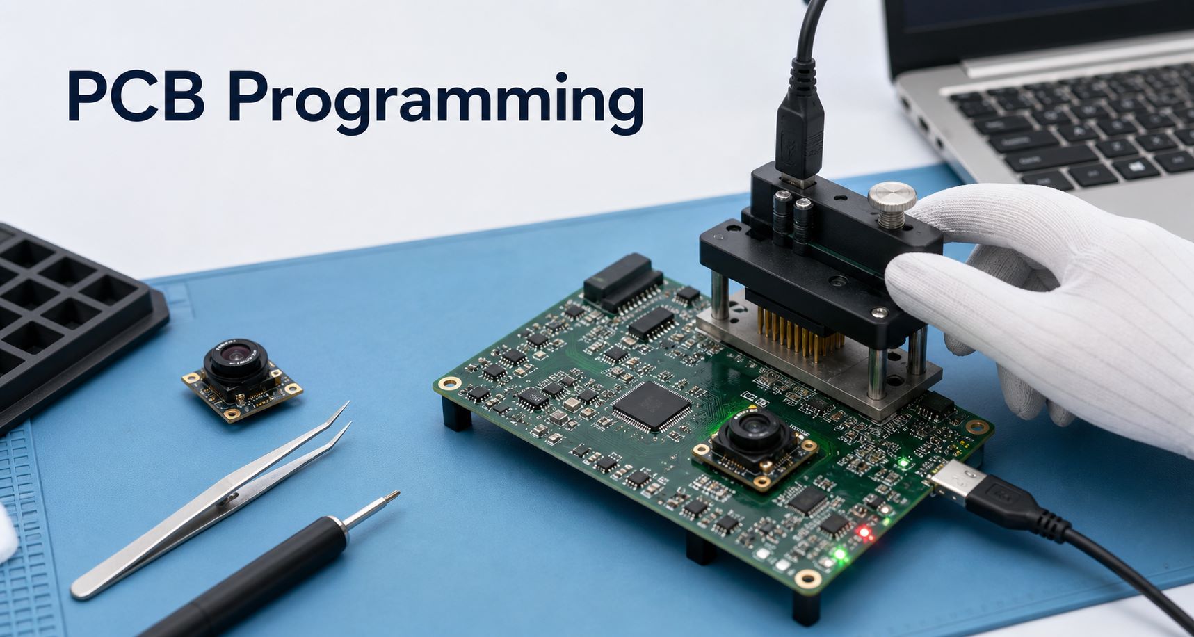
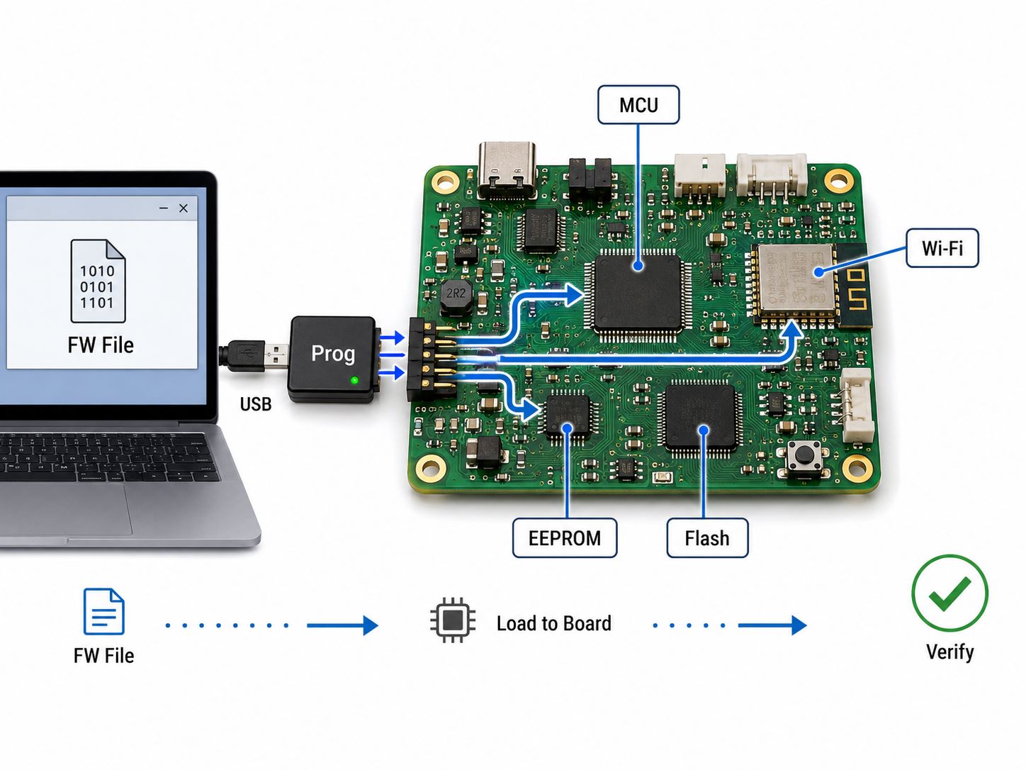
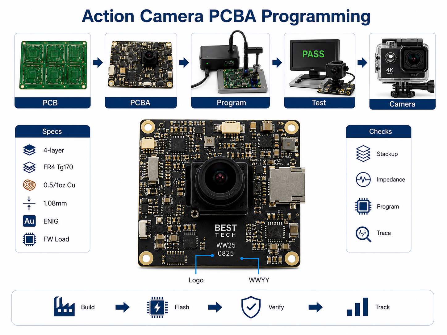
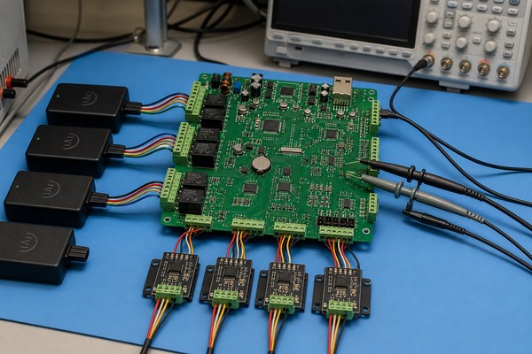
When engineers search how to program a PCB, they usually do not mean programming the bare circuit board itself. A PCB is not programmed directly. What gets programmed is the MCU, IC, EEPROM, memory device, wireless module, camera module, or other programmable component assembled on the PCB.
In real PCBA production, PCB programming usually means loading customer-approved firmware or software into assembled boards, then checking whether the programmed PCBA works according to the customer’s test method. EBest Circuit (Best Technology) supports PCB fabrication, component sourcing based on approved BOM, PCBA assembly, firmware flashing based on customer-provided files, functional testing coordination, packing, and production traceability. If you have a PCB or PCBA project that needs programming support, pls feel free to send your Gerber files, BOM, firmware file, programming instructions, test method, or assembly notes to sales@bestpcbs.com for engineering review before production.
What Does PCB Programming Mean?
PCB programming means loading software, firmware, bootloader data, configuration files, or memory data into programmable components on a PCB assembly.
Common programmable parts include:
MCU
PIC microcontroller
EEPROM
Flash memory
FPGA
Wireless module
Sensor module
Power management IC
Camera control IC
Bluetooth or Wi-Fi module
The PCB provides the physical circuit, power, signal paths, connectors, test points, and programming interface. The firmware file is usually prepared by the customer’s software or embedded engineering team.
A PCB manufacturer or PCBA assembler may help with programming during production, but that does not mean the factory writes the firmware. The factory loads the approved file, follows the customer’s programming method, and verifies the board according to the approved test procedure.
How to Program a PCB Board During PCBA Assembly
To program a PCB board during PCBA assembly, the process usually starts after SMT assembly and inspection. The board must first be assembled correctly before firmware flashing can be done reliably.
A typical PCBA programming workflow includes:
PCB fabrication
Component sourcing based on approved BOM
SMT assembly
AOI or visual inspection
IC or MCU programming
Programming result check
Functional testing
Version record and batch traceability
Packing and shipment
The programming step may happen through a programming connector, test pads, USB interface, SWD, JTAG, UART, ISP, or a custom fixture. The exact method depends on the customer’s circuit design and programming instructions.
For production, the programming file version must be clearly controlled. If different firmware versions are mixed, the product may pass assembly inspection but fail in the customer’s final system.
How to Program a Custom PCB with Customer Firmware
To program a custom PCB, the customer usually needs to provide the required firmware and production instructions. The PCBA supplier should not guess the firmware version, modify the code, or change the programming method without approval.
For a custom PCB programming project, customers should prepare:
Gerber or ODB++ files
BOM
Pick and place file
Assembly drawing
Firmware file
Programming tool or method
Programming connector definition
Test procedure
Pass/fail criteria
Firmware version requirement
Packing and labeling requirements
EBest Circuit can support firmware flashing based on customer-provided files. If the customer requires basic functional testing after programming, the test method should be confirmed before production.
For example, a programmed board may need to power on correctly, show LED status, connect through USB, display a camera image, communicate with a module, read a sensor, or pass a current consumption check. These checks should be defined by the customer and confirmed before mass production.
Can You Program a PCB Board with a Gerber File?
No. A Gerber file cannot program a PCB board.
A Gerber file is used to manufacture the bare PCB. It defines copper layers, solder mask, silkscreen, drill holes, board outline, and other PCB fabrication information. It does not contain firmware, software, or executable code.
A Gerber file can help the PCB factory make the board. To program the assembled board, you also need a firmware file or software file, plus a programming method.
In simple terms:
File Type
Purpose
Gerber / ODB++
PCB fabrication
BOM
Component sourcing
Pick and place
SMT assembly
Firmware file
IC or MCU programming
Test procedure
Functional verification
This is why PCB programming should be planned together with PCBA assembly. The PCB must include the correct programming connector, test pads, or access points before production.
How to Program a PCB Board with a USB Interface
Some PCB boards can be programmed through USB if the circuit supports it. This may be done through a USB bootloader, USB-to-UART bridge, MCU USB interface, or a customer-defined programming tool.
A USB programming process may include:
Connect the PCBA to a computer
Put the board into bootloader or programming mode
Open the customer-approved programming software
Select the correct firmware file
Flash the firmware
Verify programming success
Run a basic functional test
For production, USB programming can be convenient, but it still requires clear instructions. The factory needs to know the correct cable, software tool, driver, firmware version, programming sequence, and pass/fail standard.
If USB is also used for product operation, the customer should define whether the test is only for firmware loading or also for communication verification.
How to Program a PIC Microcontroller on a PCB
A PIC microcontroller on a PCB can usually be programmed through an ICSP interface or another customer-defined programming method. The PCB must include the correct access points for programming signals, power, ground, and reset or control lines.
For a PIC microcontroller programming project, the customer should confirm:
PIC part number
Programming interface
Pin definition
Programming voltage
Firmware file
Programmer model
Programming software
Verification method
Functional test requirement
For PCBA production, accessibility matters. If programming pads are too small, blocked by components, or difficult to contact with a fixture, programming may become slow or unreliable. This should be reviewed before mass production.
EBest Circuit can support the assembly and programming process according to customer-provided files and instructions, but firmware development and code debugging should remain with the customer’s embedded software team.
Programming Connectors, Test Points, and PCBA Fixtures
Programming access should be considered before PCB fabrication. If the board has no accessible connector or test pads, programming after assembly may become difficult.
Common programming access methods include:
Pin header
Tag-Connect style pads
Test pads
USB port
SWD connector
JTAG connector
UART pads
Bed-of-nails fixture
Custom PCBA test fixture
For prototype builds, engineers may use a connector or manual cable. For larger production, a fixture is often better because it improves speed, consistency, and operator efficiency.
A well-designed PCBA programming setup should ensure uninterrupted contact, minimize manual handling, protect the board from mechanical damage, and provide clear programming results.
PCB Programming Checks Before Mass Production
Before mass production, PCB programming should be verified with a small pilot run. This helps catch problems before a large batch is assembled.
Important checks include:
Is the firmware version correct?
Is the programming interface accessible?
Does the programming tool work consistently?
Is the programming time acceptable?
Is the pass/fail result clear?
Can the board be tested after programming?
Are labels or QR codes needed for traceability?
Is the customer’s test procedure complete?
Are failed boards handled correctly?
Is the packing method suitable after testing?
For programmed PCBA products, traceability is important. The production team should know which firmware version was loaded, which batch was programmed, which test method was used, and whether the product passed inspection.
PCB Programming Case Study for an Action Camera PCBA
A European customer needed PCB and PCBA support for an action camera project. The customer had already prepared the camera firmware and product requirements. EBest Circuit’s role was to manufacture the PCB, support assembly, load the customer-provided software, and help verify the board according to the approved test instructions.
Customer-provided firmware for action camera PCBA programming
Why this project needed careful control
The first checkpoint was the PCB structure. An action camera board usually has compact component placement, camera-related signal paths, power circuits, storage interface, connectors, and sometimes high-speed or impedance-sensitive lines. The 4-layer stackup, copper thickness, board thickness, and impedance requirement needed to be reviewed before production.
The second checkpoint was programming preparation. The customer needed the correct software loaded after assembly. That meant the firmware version, programming method, programming interface, and post-programming test steps had to be clear before production started.
The third checkpoint was production traceability. The customer required the EBest Circuit logo and WWYY production cycle marking, which helped identify the production batch. For programmed PCBA products, this is useful because the PCB batch, assembly batch, and firmware version should not become disconnected.
EBest Circuit’s support
Reviewed Gerber, BOM, stackup, impedance notes, and panel information
Confirmed FR4 Tg170, copper thickness, ENIG, solder mask, silkscreen, logo, and date code
Supported PCB fabrication and PCBA assembly in one workflow
Loaded customer-provided firmware according to customer instructions
Coordinated functional testing after programming
Checked programming result, assembly quality, and board cleanliness
Supported batch traceability for production control
For the customer, the value was not software development. The value was production execution. EBest Circuit helped connect PCB fabrication, PCBA assembly, customer-provided firmware flashing, functional testing, and batch marking in one controlled process. This reduced the risk of wrong firmware version, unclear test steps, or production handoff mistakes.
Why Choose EBest Circuit for PCB Programming Support in PCBA?
EBest Circuit is suitable for customers who need PCB manufacturing, PCBA assembly, and production programming support based on customer-approved firmware files.
Customers choose EBest Circuit because we can support:
For PCB programming projects, EBest Circuit focuses on production reliability. We help confirm files, interfaces, version requirements, test methods, and packing notes before production starts.
If you have a PCBA project that needs programming support, feel free to contact us with your Gerber files, ODB++ files, BOM, firmware file, programming instructions, test method, or assembly notes via sales@bestpcbs.com. We are here to help review the PCB and PCBA manufacturing path before production.
PCB Programming FAQs
1. Can a PCB be programmed directly?
No. A bare PCB cannot be programmed directly. The programmable parts on the PCB, such as MCU, IC, EEPROM, FPGA, or module, are programmed after assembly.
2. What do I need to program a PCB board?
You need the assembled PCB, firmware file, programming interface, programming tool, power supply method, and a clear test procedure.
3. Can a Gerber file be used to program a PCB?
No. A Gerber file is for PCB fabrication. Programming requires a firmware file or software file plus a programming method.
4. Can EBest Circuit write firmware for my PCB?
EBest Circuit mainly supports PCB manufacturing, component sourcing, PCBA assembly, firmware flashing based on customer-provided files, inspection, and testing coordination. Firmware development should be handled by the customer’s software team.
5. Can PCB programming be done during mass production?
Yes. PCB programming can be done during PCBA production if the programming interface, firmware file, test method, and version control process are confirmed before production.
Need help with PCB programming during PCBA production? Please do not hesitate to contact us with your Gerber files, BOM, firmware file, programming instructions, test method, or assembly requirements via sales@bestpcbs.com. EBest Circuit is committed to helping review the manufacturing, assembly, programming, and testing path before production starts.
Reliable access control starts at the field-wiring boundary. A door access control PCB must make every credential decision, lock command and alarm input predictable. Reader compatibility, lock current, fail-safe behavior, communication security, surge protection, power-fail recovery and production testing must be designed as one system.
EBest Circuit supports PCB design, fabrication and assembly, including prototyping and component sourcing, for custom access-control hardware. A useful quotation starts with the door count, reader protocol, lock type, input voltage, network interface, enclosure limits, firmware responsibility and acceptance-test requirements.
What Is a Door Access Control PCB?
A door access control PCB makes and executes entry decisions. It receives credential and door-status signals, applies access rules and switches the locking hardware. It may operate as a standalone panel, an intelligent network controller or an interface board connected to a larger security platform.
A door access control PCB normally connects readers, request-to-exit devices, door-position contacts, tamper switches, alarms and electric locks. Its firmware decides whether a credential and event state permit entry, records the event and drives a relay or protected solid-state output.
Standalone controller: Stores users and schedules locally and can continue operating without a server connection.
Networked controller: Exchanges users, events, time rules and health data with management software.
Door interface board: Extends reader, input and lock I/O under the supervision of a higher-level controller.
How Does a Door Access Control Circuit Board Work and What Are Its Main Components?
The board uses a closed decision chain. It reads a credential, verifies system conditions, authorizes or denies access, switches the lock and confirms the resulting door state. Breaking that chain into functional blocks makes schematic review, layout and testing easier.
Processing and memory: An MCU or MPU runs credential, schedule, event and communication logic, while nonvolatile memory protects configuration and logs.
Reader interfaces: Wiegand inputs, OSDP/RS-485 transceivers or other application-specific interfaces receive credentials and reader status.
Supervised inputs: Door contacts, request-to-exit, tamper and fire-release inputs report real field conditions and should reject noise and wiring faults.
Lock outputs: Relays or protected electronic switches control strikes, magnetic locks, bolts and alarm devices.
Power tree: Input protection, DC/DC conversion, LDO rails, brownout monitoring and optional backup-power supervision keep logic stable during lock transients.
Network and security: Ethernet, RS-485, CAN or approved wireless modules connect the controller while secure boot, protected keys and authenticated updates limit attack paths.
2-Door vs 4-Door vs Multi-Door Access Control PCB: What Is the Difference?
Door count changes the complete I/O and power architecture. Each added door multiplies reader ports, monitored inputs, lock loads, terminal density, power distribution and test coverage. Architecture should follow wiring topology and failure containment rather than fitting the maximum number of doors onto one PCB.
Controller type
Typical fit
Design focus
Main trade-off
2-door
Small sites, elevator or cabinet zones
Compact I/O, simple service access
More panels for larger sites
4-door
Commercial floors and distributed entrances
Terminal organization, relay spacing and shared power
Higher wiring and thermal concentration
Multi-door
Scalable buildings and campuses
Segmented buses, expansion I/O and fault isolation
Greater firmware, network and validation complexity
A four-door controller should still allow one faulty reader cable or lock circuit to be isolated without disabling unrelated doors. Multi-door products often benefit from a controller-plus-expansion architecture because shorter field runs, replaceable I/O modules and defined power domains simplify service.
What Are the Main Door Access Control PCB Design Requirements?
Freeze the complete requirements before selecting components. They must cover field wiring, power behavior, security, environmental limits and testability. Starting with an MCU and adding interfaces later usually creates grounding, connector and firmware constraints.
I/O matrix: Define every reader, lock, contact, exit input, alarm, tamper signal and expansion port, including inactive and fault states.
Power budget: Separate controller consumption from reader and lock loads, then evaluate startup, release, simultaneous-door and backup-power cases.
Safety behavior: Document fail-safe or fail-secure operation, fire-release interaction, manual egress and required behavior after processor or communication failure.
Cybersecurity boundary: Identify trusted devices, exposed ports, credential storage, service access, update paths and key provisioning.
Mechanical definition: Confirm enclosure, mounting holes, terminal direction, cable bend space, indicator visibility and service clearance.
Verification plan: Provide programming, test points, simulated door fixtures and pass/fail criteria before layout release.
Required input
Design action
Verification evidence
Door and I/O schedule
Map every reader, lock, door contact, exit input, tamper input and alarm channel to its normal, active, open-wire and short-wire state.
Approved I/O matrix and channel-by-channel fixture test.
Lock and reader power data
Calculate standby, startup, inrush, single-door, simultaneous-door and backup-supply loads, including cable voltage drop.
Power budget, rail measurements and brownout test record.
Reader and network protocols
Define port count, voltage, bit format or device address, baud rate, bus topology, termination and required security mode.
Interface specification and communication test log.
State-transition matrix with pass/fail acceptance criteria.
Enclosure and installation data
Lock board outline, mounting holes, terminal direction, cable bend space, airflow and service access before placement.
Mechanical drawing and enclosure-fit review.
How Should RFID, Wiegand and OSDP Reader Interface Circuits Be Designed?
Match each reader circuit to its protocol and cable environment. A generic input stage cannot satisfy every electrical and security requirement. RFID describes the credential technology; Wiegand and OSDP describe common reader-to-controller communication paths.
Wiegand inputs require defined logic thresholds, input protection, filtering and a grounding strategy appropriate to cable length and reader supply. Because implementations use different bit formats, firmware should validate format and parity rather than assume every reader is identical. OSDP uses an RS-485 physical layer and supports supervised bidirectional communication. OSDP compatibility alone does not prove that Secure Channel is active; configuration and bench testing must verify the required security mode.
Protect the connector first: Place ESD and transient components close to the reader terminal before traces enter the logic area.
Control the RS-485 bus: Plan termination, biasing, topology, common-mode range and reference conductor from the complete cable installation.
Separate power noise: Do not route reader data alongside relay contacts, lock-current loops or switching-node copper.
Support service diagnosis: Expose protocol, supply and ground test points without creating an unsecured debug path.
Decision point
Wiegand
OSDP
Communication
Simple one-way data signaling with implementation-specific credential formats.
Addressed, bidirectional communication over an RS-485 physical layer.
Monitoring
Limited interface supervision; wiring faults may need separate detection.
Supports supervised communication and reader status reporting.
Security planning
Useful for legacy compatibility, but credential data is not protected by the interface itself.
Secure Channel can protect reader-panel traffic when correctly configured and verified.
Best fit
Existing readers, controlled migration and products that must retain legacy support.
New designs that need interoperability, diagnostics, multidrop capability and stronger communication security.
How Should the Door Lock Control Circuit, Relay Output and Power Supply Be Designed?
Size the lock-control stage from the real load profile. Include steady-state current, inrush, release behavior and the fail-safe requirement, not only the nameplate voltage. Relay contacts can provide useful isolation, while MOSFET outputs can add diagnostics and fast protection.
Confirm the load: Record lock type, nominal voltage, steady current, inrush, release time and fail-safe or fail-secure behavior.
Select the output: Use dry relay contacts when isolation and polarity flexibility are required; consider protected MOSFET outputs when diagnostics, switching speed or electronic current limiting are needed.
Control inductive energy: Match the flyback diode, TVS or clamp network to the load and required release time. A simple diode lowers voltage stress but can slow release.
Protect each channel: Coordinate contact rating, conductor width, terminal rating, fuse or resettable protection and short-circuit recovery.
Protect the logic rail: Include cable voltage drop and simultaneous lock events in the power budget so a door command cannot reset the processor or corrupt event memory.
Power sequencing should define startup, battery switchover, brownout and restart behavior. The design review must also state whether an emergency input removes lock power in hardware, firmware or both, according to the system requirements and local regulations. Verification should record rail voltage, processor reset status, relay state and event-memory integrity during each transition.
How to Protect a Door Access Control Board from ESD, Surge and Wiring Faults?
Use layered protection at every field port. Limit energy at the connector, control current, prevent reverse paths and keep residual transients away from logic. One TVS diode added late in layout is not a complete protection plan.
ESD path: Use short, low-inductance connections from the protective device to the intended reference or chassis path.
Surge coordination: Select TVS, series impedance, fusing and downstream ratings so each layer survives the expected waveform.
Miswiring tolerance: Evaluate reverse polarity, reader power shorts, lock-output shorts, cross-connected terminals and hot-plug events.
Galvanic and ground strategy: Decide where isolation is necessary and avoid accidental return paths through communication shields or mounting hardware.
Recovery behavior: Verify that a protected fault clears safely and does not leave a relay, processor or communication port in an undefined state.
How Should a Networked Access Control Board Be Designed for Secure Communication?
Secure communication begins with a protected device identity. It also requires authenticated sessions, controlled updates and safe local operation when the network is unavailable. Adding Ethernet or Wi-Fi without defining trust boundaries increases the attack surface.
Protect device identity: Provision a unique device identity and keep long-term keys in a protected device or secure region.
Authenticate code and updates: Verify firmware before execution, accept updates only from authorized sources and prevent an interrupted or failed update from leaving an unusable controller.
Reduce exposed interfaces: Disable unnecessary production debug access, limit services and separate installer, administrator and application permissions.
Use standard security protocols: Authenticate management sessions, protect data in transit, rate-limit repeated attempts and record security-relevant events.
Define offline operation: Specify which cached users and schedules remain valid, how clock integrity is maintained, how many events can be stored and how records are synchronized after reconnection.
What PCB Materials, Stackups and Layout Rules Are Suitable for Access Control Boards?
Choose material and stackup from the application requirements. Most controllers can use a suitable FR-4 construction, but layer count and material grade should follow routing density, EMC, operating temperature and reliability needs. Confirm the construction against the actual product specification.
A four-layer stackup often gives a continuous ground reference and cleaner power distribution than a crowded two-layer board. Keep the network magnetics or transceiver region, processor, reader interfaces, switching regulators and relay contacts in clear functional zones. Do not split the return path beneath high-speed or noise-sensitive traces. Provide creepage and clearance appropriate to the actual working voltage, pollution environment and governing safety requirements.
Field terminals: Place protection and filtering beside the connector and label channels consistently.
Relays and lock power: Separate contact copper from low-voltage logic and control heat around high-current connections.
Ethernet or RF: Follow the transceiver/module reference layout, impedance and keep-out requirements.
Manufacturing access: Provide fiducials, programming pads, test points and realistic probe clearance.
Stackup choice
Suitable use
Release check
Two layers
Lower-density controllers with modest interface speed and enough area for uninterrupted return paths.
Confirm grounding, relay-current routing, thermal paths and EMC margin on the finished layout.
Four layers
Networked or denser boards that benefit from a continuous ground plane and more controlled power distribution.
Approve the stackup, reference planes, impedance needs, via structure and fabrication availability before routing.
More than four layers
Use only when routing density, memory buses, RF, isolation or mechanical constraints justify the added process complexity.
Document the electrical reason for each added layer and verify manufacturability with the selected supplier.
How Are Door Access Control PCBs Manufactured and Assembled?
Use a controlled release-to-acceptance sequence. Manufacturing should progress from engineering-data review through fabrication, assembly, programming and functional acceptance. Terminal blocks, relays, tall capacitors and network connectors make process planning as important as the SMT stage.
Engineering data and DFM review: Check Gerber or ODB++, NC drill, stackup, fabrication drawing, BOM, centroid data, polarity, assembly drawings, firmware and test instructions; issue one consolidated question list before release.
Bare PCB fabrication: Build the approved stackup, image and etch copper, drill and plate holes, apply solder mask and finish, route the profile, then complete electrical test and dimensional inspection.
Incoming component verification: Confirm relay contact ratings, protection-device identity, connector pitch, polarized parts, moisture sensitivity and approved substitutions against the released BOM.
Solder-paste printing and SPI: Verify paste volume and alignment before placement, with stencil apertures reviewed for fine-pitch and thermal-pad components.
SMT placement and reflow: Place components using the approved centroid and polarity data, then control the reflow profile for the actual component and board mix.
Through-hole assembly: Install relays, terminal blocks and other tall or high-current parts using the defined selective-solder, wave-solder or controlled hand-solder process.
Inspection: Use AOI for visible SMT joints and polarity; apply risk-based X-ray to hidden or bottom-terminated joints when the package and acceptance plan require it.
Programming and functional acceptance: Load the approved firmware, provision required unit data and run the reader, input, relay, network, power-transition and fault tests before release.
EBest Circuit’s service scope covers PCB design, production and assembly, including prototype builds and component sourcing. Available material and product experience includes FR-4, multilayer, high-Tg, high-speed and impedance-control PCB families; the final construction and process remain subject to project review.
What Testing Is Required for a Door Access Control PCB Assembly?
Test every channel and critical state transition. A processor boot test alone is insufficient. A production fixture should simulate readers, door contacts, exit inputs, lock loads, network traffic, power interruption and fault conditions with recorded pass/fail limits.
Bare-board checks: Electrical test and fabrication inspection confirm continuity, isolation, dimensions and specified construction.
Assembly inspection: SPI, AOI and risk-based X-ray identify paste, placement and solder-joint defects.
Programming and identity: Load approved firmware, protect production interfaces and record the required unit identifiers.
I/O functional test: Exercise all readers, supervised inputs, relays, indicators, buzzers and expansion channels.
Power and fault test: Check startup, brownout, backup transition, shorted field ports, reversed input and simultaneous lock events as specified.
Communication test: Verify Ethernet/serial links, OSDP behavior, reconnect logic and the required secure session functions.
A repeatable production test needs more than a technician’s visual judgment. The released fixture package should identify connector pinout, simulated loads, firmware version, measurement points, numerical limits, expected relay and indicator states, failure codes and the records retained for each unit. A known-good reference assembly helps confirm that fixture maintenance has not changed the test result.
What Custom Door Access Control PCB Manufacturing and Assembly Services Can We Provide?
Define custom support through measurable deliverables. It can cover design files, prototype risk reduction, sourced components, assembled controllers and repeatable production data. This is more useful than a vague turnkey promise.
Design support: Schematic and layout review for reader interfaces, lock outputs, power integrity, protection, stackup and test access reduces avoidable respins.
Prototype build: A controlled sample build exposes connector, programming, firmware and fixture issues before volume tooling is fixed.
Component sourcing: BOM review and approved substitution control protect electrical ratings and firmware compatibility.
Fabrication and assembly: One coordinated data package reduces responsibility gaps between bare-board and PCBA suppliers.
Fast-delivery review: EBest Circuit offers expedited service, including urgent bare-board shipment within 24 hours when the material, complexity, quantity and production data make that schedule feasible.
Quality evidence: EBest Circuit lists ISO 9001:2015, ISO 13485:2016, IATF 16949, AS9100D, UL, RoHS and REACH; each order should identify which certification scope, inspection records and acceptance criteria are relevant.
To shorten engineering review and quotation time, submit one controlled package containing the current PCB data, BOM, quantities, reader and lock specifications, enclosure drawing, firmware responsibility, programming method and acceptance test. Clearly mark unresolved items and approved alternatives so they can be closed before material purchasing begins.
4-Door Networked Access Control PCB Manufacturing and Assembly Case Study
A credible case needs a traceable evidence chain. This representative project shows how an incomplete four-door controller package can become a controlled build release without claiming an unverified customer identity, yield, delivery result or field-performance figure.
Project Background: A security-equipment team required one board to manage four doors, exchange events with network software and retain defined local operation during a server interruption. The hardware included four reader channels, monitored door and exit inputs, four lock outputs, Ethernet, nonvolatile event memory and a protected DC input.
Project Requirements: The team supplied Gerber/ODB++, NC drill, stackup, BOM, centroid data, assembly drawings, firmware and an initial functional-test description. Before release, the requirements matrix still needed confirmed lock voltage and inrush, Wiegand/OSDP allocation, RS-485 termination, emergency-release logic, offline user and event limits, enclosure clearances and production-key handling.
Our Solution: Engineering converted those open items into one tracked question list and held fabrication until the electrical and mechanical answers were approved. The layout review separated reader, Ethernet, logic, regulator and relay-current zones; checked current paths, terminal ratings and protection placement; and aligned programming and measurement pads with the fixture. The process plan then defined SMT, through-hole relay and terminal assembly, AOI, risk-based X-ray, controlled provisioning and four-channel functional testing.
Output Results: The release package contained the approved design revision, resolved engineering-question log, controlled BOM, fabrication and assembly data, programming instructions, fixture connection map and pass/fail test definition. Fabricated boards and assembled units could therefore be checked against the same revision and acceptance criteria, while the retained package established a traceable baseline for repeat orders.
Why Choose EBest Circuit as Your Door Access Control PCB Manufacturer?
Choose a partner that closes responsibility gaps. Access-control requirements must become reviewable files, controlled parts, testable assemblies and clear responsibility boundaries. Company history or certificate names alone do not prevent a door-controller failure.
One engineering path: Coordinating design, fabrication, sourcing and assembly reduces handoff gaps when a reader, relay, connector or firmware requirement changes.
Prototype-to-production continuity: Keeping approved files, substitutions and test requirements together reduces the chance that a corrected sample issue returns in volume builds.
Application-matched construction: Access to FR-4, multilayer, high-Tg, high-speed and impedance-control PCB options supports selection based on the actual network, thermal and mechanical requirements.
Order-specific quality planning: Listed management-system and product-compliance credentials can support supplier qualification, while each order still defines its own inspection, traceability and acceptance evidence.
Feasible expedited planning: Early material and process review turns a general fast-delivery request into a schedule that identifies the real start condition and remaining risks.
EBest Circuit can review the controller architecture and manufacturing package before quotation, helping the project team identify missing power, interface, test and sourcing details early.
FAQs About Door Access Control PCBs
These questions cover procurement and implementation details that are useful but do not repeat the main design sections.
Q1: What files are needed to quote a door access control PCB assembly?
A1: Submit Gerber or ODB++, NC drill, BOM, centroid data and assembly drawings first. Add the stackup, firmware, programming method, test procedure, quantities and approved-substitution rules so fabrication and PCBA scope can be reviewed together.
Q2: How should event logs be protected during sudden power loss?
A2: Use power-fail detection, bounded write operations and a storage method that tolerates interrupted updates. Testing should remove input power at different points in an event write, then confirm that existing records, the newest valid record, indexes and the restart state remain consistent.
Q3: What environmental tests are useful for an access control controller?
A3: Select tests from the declared installation environment and product requirements. Useful checks may include operating-temperature cycling, humidity exposure, powered thermal testing, vibration where relevant and repeated connector or relay operation. Test limits and acceptance criteria must come from the actual product specification.
Q4: How should the real-time clock and time synchronization be validated?
A4: Verify time accuracy, backup retention, timezone handling and recovery after network and power interruptions. The test plan should also check daylight-saving behavior where applicable, server resynchronization and the order of event records created before and after a clock correction.
Q5: How should a tamper input be handled?
A5: Treat tamper as a supervised security input with a defined normal, alarm and wiring-fault state. Its circuit, polling and event handling should match the enclosure and system threat model.
Q6: Is conformal coating required for access control boards?
A6: Coating is application-dependent, not an automatic requirement. Review humidity, condensation, contamination, connector masking, repairability and coating compatibility, then specify the material and inspection criteria if needed.
Q7: Can relays be replaced by MOSFET outputs?
A7: Sometimes, but the electrical behavior and isolation are different. Compare polarity, load type, leakage, diagnostic needs, transient energy, fail-state behavior and service expectations before changing the output topology.
Q8: How are unique device credentials programmed during production?
A8: Use a controlled provisioning process that writes and verifies unit-specific data without exposing reusable secrets. The factory test plan should define access control, logging, reject handling and debug-port closure.
Q9: What causes intermittent reader communication after installation?
A9: Common causes include wiring topology, grounding, termination, voltage drop, noise coupling and protocol configuration. Capture cable length, reader type, power at the reader and communication errors before blaming firmware or the PCB.
Q10: How should component substitutions be controlled for a repeat order?
A10: Maintain an approved BOM and require technical review before any substitute is released. Relays, TVS devices, transceivers, memory and connectors can alter ratings, firmware behavior or mechanical fit even when packages appear compatible.
Conclusion
A reliable door access control PCB starts with a complete I/O, power, security and failure-behavior definition. Reader interfaces, lock loads, field protection, network security, PCB layout and production tests must then be verified as one control chain.
An early engineering review can expose reader-interface, lock-power, protection, enclosure and test-fixture risks before they become prototype respins or production delays. EBest Circuit can coordinate design review, PCB fabrication, component sourcing, assembly, programming preparation and order-specific testing through one controlled project package.
For custom door access control PCB design, prototyping, fabrication, component sourcing and assembly, send your Gerber/ODB++, NC drill, stackup, BOM, centroid data, firmware, quantities and test requirements to sales@bestpcbs.com for engineering review and a quotation.
A 2.4GHz PCB antenna is commonly used in Wi-Fi, Bluetooth, Zigbee, IoT wireless modules, smart sensors, gateways, medical electronics, wearable devices, and compact connected products. It allows wireless communication without adding a separate external antenna, but it also makes the PCB layout and manufacturing process more sensitive.
For EBest Circuit (Best Technology), the focus is not to design the antenna from zero or replace the customer’s RF engineering work. Our role is to manufacture and assemble the PCB according to customer-approved design files, while helping review manufacturability risks around the antenna area, RF feed line, material, surface finish, impedance notes, SMT assembly, inspection, and testing requirements. If you are preparing a 2.4GHz PCB antenna board, send your Gerber files, ODB++ files, stackup, BOM, drawings, module datasheet, or assembly notes to sales@bestpcbs.com for engineering review before production.
What Is a 2.4GHz PCB Antenna?
A 2.4GHz PCB antenna is an antenna structure formed directly on the printed circuit board. Instead of using only an external antenna, the board itself includes a copper antenna pattern that operates around the 2.4GHz frequency band.
This frequency band is extensively used by:
Wi-Fi
Bluetooth
BLE devices
Zigbee
Thread
Some IoT wireless modules
Smart home products
Wireless sensors
Compact industrial devices
The antenna may appear as a meandered trace, inverted-F antenna, chip antenna connection area, patch-style antenna structure, or another customer-defined antenna pattern. The exact antenna geometry should be defined and validated by the customer’s RF design team or module supplier. During PCB manufacturing, the board supplier must protect this geometry and avoid process changes that may affect performance.
How Does a 2.4GHz Antenna PCB Work?
A 2.4GHz antenna PCB works by using copper geometry on the PCB to radiate and receive electromagnetic signals. The antenna area, feed line, ground reference, keep-out zone, material, board thickness, nearby components, and enclosure can all affect wireless performance.
From a PCB manufacturing point of view, several areas matter:
Area
Why It Matters
Antenna geometry
Must match customer-approved files
Keep-out area
Avoids unwanted copper or metal interference
RF feed line
May require impedance control
Ground reference
Supports stable RF behavior
Material
Affects dielectric properties
Surface finish
Affects soldering and long-term reliability
Assembly
Components near antenna may affect performance
The PCB manufacturer should not casually modify the antenna trace, copper pour, ground clearance, or feed area. Even small changes may affect tuning, signal strength, or final wireless performance.
Common Types of 2.4GHz PCB Antennas
Different products may use different 2.4GHz PCB antenna styles. The choice is usually made by the customer’s RF engineer, wireless module supplier, or reference design provider.
Common types include:
Meandered PCB antenna A compact trace antenna often used when board space is limited. It can be useful for Bluetooth, BLE, and small IoT devices.
Inverted-F antenna A common PCB antenna type for 2.4GHz wireless products. It usually requires careful control of the antenna shape, feed point, ground, and keep-out area.
PCB patch antenna A patch antenna structure may be used when the project needs a defined radiation direction or board-level antenna area.
Chip antenna with PCB matching area Some products use a ceramic chip antenna or module antenna. Even in this case, the PCB layout around the chip antenna, ground clearance, feed line, and matching components still matters.
External antenna connector design Some 2.4GHz products use an RF connector such as IPEX/U.FL or SMA. The PCB still needs proper RF feed line routing, connector footprint, soldering quality, and mechanical stability.
EBest Circuit manufactures the PCB or PCBA according to the customer-approved 2.4 GHz antenna PCB design, module supplier recommendations, Gerber files, stackup, and production notes.
2.4GHz PCB Antenna Design Files and Manufacturing Checks
The phrase 2.4GHz PCB antenna design can mean many things. For some engineers, it means antenna simulation and RF tuning. For a PCB manufacturer, the practical focus is different: whether the approved antenna design files can be manufactured and assembled without introducing avoidable risk.
Before production, EBest Circuit can help review:
Gerber or ODB++ files
Stackup and board thickness
Material requirement
Copper thickness
Antenna keep-out area
RF feed line notes
Controlled impedance requirements
Solder mask openings
Surface finish
Module footprint
Connector footprint
Panelization
Test points and inspection notes
If the customer provides a wireless module datasheet or reference layout, it should be checked against the actual PCB files. This helps reduce mismatches between the intended RF layout and the board that will be produced.
2.4GHz WiFi PCB Antenna Layout Areas to Protect
A 2.4GHz WiFi PCB antenna is sensitive to its surrounding area. Even if the antenna pattern is correct, the final board may still perform poorly if the keep-out area, ground, enclosure, connector, or nearby components are not controlled.
Important areas to protect include:
Area
Manufacturing Concern
Antenna copper
Do not change shape or length
Keep-out zone
Avoid copper, vias, or components
Feed line
Follow impedance and width notes
Ground clearance
Match approved layout
Matching circuit
Preserve pad and component positions
RF connector
Control soldering and alignment
Board edge
Avoid outline changes near antenna
The PCB factory should not add copper balancing, tooling marks, vias, labels, or panel rails inside the antenna keep-out zone unless the customer confirms it. For antenna products, small “helpful” edits can become performance risks.
2.4GHz Patch Antenna PCB vs Meandered PCB Antenna
A 2.4GHz patch antenna PCB and a meandered PCB antenna serve different layout and product needs.
Antenna Type
Typical Use
Patch antenna PCB
Larger antenna area, more directional behavior
Meandered PCB antenna
Compact products and space-saving layouts
Chip antenna layout
Small devices using supplier-defined antenna parts
External antenna connector
Products needing detachable or higher-gain antenna options
For PCB manufacturing, the key is not to decide which antenna type is best. That decision belongs to the customer’s RF design team. The PCB manufacturer’s responsibility is to keep the approved antenna structure, material, copper, surface finish, and board outline consistent with the production files.
This is especially important for products such as IoT sensors, wireless gateways, Bluetooth devices, smart home controllers, medical wearables, and compact industrial modules.
PCB Material and Surface Finish for 2.4GHz PCB Antenna Boards
Many 2.4GHz PCB antenna boards are made with FR4, especially for common IoT, Bluetooth, Wi-Fi, and smart device products. However, material selection still matters because dielectric properties, board thickness, copper thickness, and stackup can affect RF behavior.
Common manufacturing points include:
FR4 material grade
Tg requirement
Board thickness tolerance
Copper thickness
Solder mask type
ENIG or other surface finish
Controlled impedance requirement
RF feed line geometry
Consistent production stackup
ENIG is often selected when the project needs good solderability, flat pads, fine-pitch assembly, or better surface stability. For cost-sensitive products, other surface finishes may also be possible, but the choice should match the assembly process and product reliability requirements.
For high-volume or high-reliability wireless products, production consistency matters. A prototype that works well should not become unstable in batch production because of uncontrolled material or stackup changes.
PCBA Assembly Risks for 2.4GHz PCB Antenna Products
PCBA assembly can affect 2.4GHz PCB antenna products even when the bare PCB is correct. The module, RF connector, matching components, shield, crystal, sensor, power circuit, and nearby components must be assembled consistently.
Insufficient inspection around small passive components
Testing notes missing from production files
EBest Circuit can support PCB SMT assembly, connector assembly, component sourcing based on approved BOM, AOI inspection, X-ray inspection when needed, functional testing coordination, and packing. For RF performance testing or wireless certification, the customer usually defines the test method or works with a dedicated RF test lab. EBest Circuit can coordinate production testing according to approved customer instructions.
2.4GHz PCB Antenna Board Manufacturing Case Study
A customer from Europe needed a small flexible PCB used in a compact 2.4GHz wireless product. The antenna-related structure and circuit files were already defined by the customer. EBest Circuit’s role was to manufacture the FPC according to the approved files and control the details that could affect assembly, connection reliability, and product fit.
Project requirements
2-layer FPC
0.5oz RA copper
Finished thickness: 0.15mm
Finger opening area: 0.30mm
PI stiffener and FR4 stiffener
Customer-approved antenna-related layout
Flexible connection area for compact assembly
Why this project needed careful review
This project looked small, but it had several details that needed control. The 0.15mm FPC thickness affected flexibility and installation fit. The 0.5oz RA copper was important for bending reliability because rolled annealed copper is often preferred for flexible circuits that need better ductility.
The finger opening area also needed careful manufacturing control. If the opening was not accurate, it could affect contact reliability during assembly. The PI and FR4 stiffeners had to be placed correctly to support the connection area and protect the flexible section from unnecessary stress.
EBest Circuit’s manufacturing support
Reviewed FPC files before production
Confirmed 2-layer FPC structure and 0.15mm finished thickness
Controlled 0.5oz RA copper requirements
Checked finger opening area and stiffener position
Manufactured PI and FR4 stiffener areas according to customer files
Protected the approved antenna-related layout during production preparation
For the customer, the value was not antenna redesign. The value was precise FPC manufacturing. The board had to remain flexible where bending was needed, reinforced where connection support was required, and consistent with the customer-approved 2.4GHz wireless product files. This helped the customer move the compact wireless product toward assembly and validation with fewer manufacturing risks.
Why Choose EBest Circuit for 2.4GHz PCB Antenna PCB and PCBA?
EBest Circuit is suitable for customers who already have approved 2.4GHz PCB antenna design files and need reliable PCB manufacturing, component sourcing, PCBA assembly, and production support.
Customers choose EBest Circuit because we can support:
PCB fabrication
DFM review before production
Stackup and material review
Controlled impedance review when required
ENIG and other surface finish options
Component sourcing based on approved BOM
SMT assembly
Connector assembly
AOI and inspection support
Functional testing coordination
Prototype and small-batch production
One-stop PCB + sourcing + assembly service
For 2.4GHz antenna board projects, EBest Circuit pays special attention to antenna keep-out areas, RF feed line notes, module footprints, connector positions, surface finish, panelization, and assembly reliability. These details help reduce manufacturing risk without crossing into unsupported RF antenna design work.
If you are preparing a 2.4GHz PCB antenna board, send your Gerber files, ODB++ files, stackup, BOM, module datasheet, drawings, or assembly notes to sales@bestpcbs.com. Our engineering team can help review the PCB and PCBA manufacturing path before production starts.
FAQs about 2.4GHz PCB Antenna
1. What is a 2.4GHz PCB antenna?
A 2.4GHz PCB antenna is an antenna structure made from copper traces on the PCB. It is often used in Wi-Fi, Bluetooth, BLE, Zigbee, and IoT wireless products.
2. Can EBest Circuit design a 2.4GHz PCB antenna from zero?
EBest Circuit mainly supports PCB manufacturing, DFM review, component sourcing based on approved BOM, PCBA assembly, inspection, and testing coordination. We manufacture and assemble according to customer-approved antenna design files and production requirements.
3. Why is the antenna keep-out area important?
The antenna keep-out area helps prevent unwanted copper, vias, components, metal parts, or panel features from affecting wireless performance. It should follow the approved antenna layout or module supplier recommendation.
4. What surface finish is suitable for 2.4GHz PCB antenna boards?
ENIG is widely used when the project needs flat pads, good solderability, fine-pitch assembly, or reliable surface quality. The final choice should match the assembly and product requirements.
5. What files should I send for a 2.4GHz PCB antenna board project?
You can send Gerber or ODB++ files, stackup, BOM, drawings, module datasheet, antenna layout notes, impedance notes, placement file, assembly notes, and testing requirements.
Need help with a 2.4GHz PCB antenna board project? Pls feel free to send your Gerber files, ODB++ files, stackup, BOM, drawings, module datasheet, or assembly requirements to sales@bestpcbs.com. EBest Circuit’s engineering team can help review the PCB and PCBA manufacturing path before production.
Quick turn PCB boards shorten the path to testable hardware. That speed matters only when the fabrication data are complete, the stackup is manufacturable, components are available and inspection requirements are defined before work starts. For urgent PCB projects, EBest Circuit coordinates design support, prototyping, fabrication, component sourcing and assembly through one technical contact.
What Are Quick Turn PCB Boards?
Quick turn PCB boards use an expedited production schedule. They are commonly used for prototypes, engineering validation, urgent replacement builds and low-volume product iterations. “Quick turn” is not one universal number: it may describe bare-board fabrication only, fabrication plus assembly, or the entire interval through shipment.
A useful quotation names both the starting and finishing events. Fabrication time normally starts after the files pass engineering review and all commercial questions are closed. Assembly time may start only after the boards, stencil data and approved components are available. Factory time and shipping time belong on separate lines.
How Long Does Quick Turn PCB Manufacturing and Assembly Take?
Bare boards can take 24 hours to 10 working days. Complete turnkey PCB fabrication and assembly commonly needs 7–15 working days. The shortest window applies to small quantities of standard rigid boards with approved data and available materials. Fabrication time starts after engineering questions are closed; assembly time starts after the last required component is available.
Quick-Turn Order
Typical Factory Time
When the Time Applies
1–2 layer rigid FR-4 bare PCB
24–48 hours
Small prototype quantity, standard material, standard finish and no unresolved DFM issue
4 layer rigid FR-4 bare PCB
2–3 working days
Approved standard stackup, conventional through vias and material in stock
6–8 layer rigid multilayer PCB
3–5 working days
Stackup and impedance structure approved before CAM release
10+ layer, HDI or sequential-lamination PCB
5–10 working days
Depends on microvia cycles, via filling, special laminate and inspection requirements
Simple flex PCB
3–7 working days
Stock polyimide, simple outline, conventional coverlay and limited layer count
Rigid-flex or complex flex PCB
7–15 working days
Material, stiffener, bend-area, lamination and via structure fully approved
Assembly only with all parts consigned
2–5 working days
Boards, stencil data and complete component kit have arrived and passed incoming check
Turnkey PCB fabrication and assembly
7–15 working days
BOM is approved and every component is available; programming and testing may add time
These ranges are planning references, not unconditional promises. EBest reports that eligible urgent bare-board orders can be shipped within 24 hours, but the exact commitment must be confirmed after reviewing layer count, materials, quantity, design rules, inspection scope and current capacity. Courier transit and customs clearance are separate from factory time.
What Factors Affect Quick Turn PCB Lead Time and How Can Delays Be Avoided?
The longest unresolved task controls lead time. A rush fee cannot compensate for an unavailable laminate, an obsolete IC or a stackup that has not been approved. The schedule is easier to protect when every risk has a named action, responsible contact and deadline.
Layer count and lamination cycles: every multilayer pressing cycle, blind/buried-via sequence or HDI buildup adds fixed process time. Avoid delay by approving a manufacturable stackup before order release.
Material availability: special high-frequency laminates, unusual thicknesses, heavy copper and uncommon solder-mask or finish combinations may require procurement. Confirm stock or approve an electrically suitable alternative first.
Design-rule exceptions: fine traces, small annular rings, high aspect ratios, tight solder-mask dams and copper-to-edge conflicts trigger engineering questions. Run DFM before starting the clock.
Controlled impedance: the fabricator may need to adjust trace width for the selected laminate and finished copper. Provide target impedance, tolerance and reference layers, then authorize one approver to sign off quickly.
Component shortages: one unavailable connector or programmed IC can stop an entire PCBA. Lock manufacturer part numbers, identify acceptable alternates and review lifecycle status before ordering.
Revision control: mismatched Gerber, drill, BOM and centroid revisions cause holds or wrong builds. Put the same revision and release date on every file and withdraw superseded packages.
Test preparation: functional tests can be delayed by missing firmware, cables, fixtures or acceptance limits. Release test assets with the production package, not after assembly.
Approval response: unanswered engineering questions leave material and machines idle. Nominate a technical contact who can approve stackup, substitutes and deviations within the same working day.
A practical schedule lists five milestones: data approval, material/component readiness, bare-board completion, assembly/test completion and shipment. With those dates visible, a delay can be traced to engineering, procurement, production or logistics.
What PCB Types and Technologies Support Quick Turn Production?
Many PCB technologies can use quick-turn production. EBest’s product range covers the technologies below; each urgent build still needs material and construction review.
PCB Type or Technology
Suitable Quick-Turn Work
What Must Be Confirmed
Single-sided and 2–8 layer FR-4
Prototype, design revision, pilot build and replacement board
Standard stackup, copper weight, finish and drill rules
Multilayer and controlled-impedance PCB
High-speed controller, communication and computing prototypes
Layer order, dielectric thickness, impedance targets, coupons and tolerance
HDI and extra-thin PCB
Dense portable, sensor and compact control electronics
Microvia structure, sequential lamination, via fill, fine-line capability and handling
Flex and semi rigid-flex PCB
Cable replacement, moving interconnect and space-limited prototypes
Polyimide, coverlay, stiffeners, bend zones and dimensional tooling
Rigid/flex transition, no-flow material, coverlay, via placement and lamination sequence
Metal-core, busbar and heavy-copper PCB
LED, power conversion, motor control and high-current evaluation
Base metal, dielectric system, copper thickness, thermal path and profiling method
Ceramic PCB
Power module, high-temperature and compact thermal prototypes
Alumina/AlN substrate, metallization, copper structure and available panel format
RF, high-frequency and high-speed PCB
RF front end, antenna feed, radar and high-speed link evaluation
Specified laminate, Dk/Df basis, surface finish, impedance and RF test coupon
High-Tg and impedance-control PCB
Thermally demanding or signal-sensitive industrial builds
Exact laminate grade, Tg requirement, stackup and measurable acceptance criteria
For the fastest route, provide both the preferred construction and the electrical or mechanical requirement behind it. Compare the design with the supplier’s verified PCB manufacturing capability. Engineering can then determine whether an in-stock material or standard build achieves the same function without introducing a new qualification risk.
What Files Are Required for a Quick Turn PCB Online or Instant Quote?
Reliable quotes require a complete build package. Use one ZIP file with a clear revision name, remove obsolete outputs and include a short read-me that identifies quantity, requested factory date and the authorized technical contact.
Fabrication image data: a complete PCB Gerber file package in RS-274X, ODB++ or another agreed intelligent format covering every copper, solder-mask, legend and paste layer.
NC drill and route data: separate plated and non-plated drills where applicable, slots, countersinks, depth-controlled features and the final board outline.
Fabrication drawing: finished dimensions, tolerances, layer order, material, finished thickness, copper weight, surface finish, solder-mask/legend requirements, via treatment and special notes.
Stackup and impedance table: signal/reference layers, target ohms, tolerance, trace type and any differential pair requirement. State whether the fabricator may adjust geometry.
Panel requirement: individual board or array, rail width, breakaway method, tooling holes, fiducials and any assembly-panel constraints.
Assembly BOM: reference designators, quantity, value, package, manufacturer, exact MPN, approved alternative and do-not-substitute status.
Centroid/pick-and-place file: X/Y position, rotation, board side and reference designator using the same origin and revision as the assembly drawing.
Programming and test package: firmware version, programming steps, connectors, power limits, fixture/cable definition, test sequence, pass/fail limits and required records.
Commercial inputs: bare-board and assembled quantities, acceptable overage, consigned parts list, delivery destination, shipping terms and requested date.
Before uploading, view the final package and check layer alignment, mirrored bottom data, drill registration, outline closure, polarity and BOM-to-centroid consistency. Name every file with the same project and revision identifier. If the quote tool cannot represent a special requirement, write it in the fabrication drawing and request manual engineering review rather than selecting the closest option.
How Does the Quick Turn PCB Manufacturing Process Work?
Quick-turn builds still use the complete fabrication route. Physical operations such as lamination, plating, curing and testing cannot simply be skipped or shortened below their controlled process window.
Order and revision intake: confirm quantity, delivery target, fabrication format, drawing, stackup and revision. CAM should stop if the drill, outline or drawing conflicts with the image data.
DFM and stackup review: check trace/space, annular ring, drill-to-copper distance, hole aspect ratio, copper balance, solder-mask clearance, controlled impedance and panel utilization. Return one consolidated engineering-question list.
CAM tooling and panelization: generate production panels, tooling holes, fiducials, test coupons, drill programs and rout/V-score paths. Apply controlled compensation for etching, plating and finished dimensions.
Material cutting and preparation: allocate the approved laminate, prepreg and copper foil; cut panels and prepare copper surfaces. Material identity must match the traveler before imaging.
Inner-layer imaging and etching: transfer internal circuitry, develop and etch unwanted copper. AOI compares the finished inner layers with CAM data before they become inaccessible inside the multilayer structure.
Oxide treatment and lamination: prepare inner-layer copper, stack cores and prepregs in the correct order, then press under the qualified heat and pressure cycle. Multilayer registration is checked after lamination.
Mechanical or laser drilling: drill through holes, blind/buried vias, microvias, slots and tooling features according to the released program. Deburr and desmear holes so the plating can form a reliable interconnect.
Electroless copper and electroplating: deposit conductive copper in the hole walls, then build the specified copper thickness. Plating uniformity, hole-wall condition and copper thickness are process-control points.
Outer-layer imaging and etching: form the external circuitry and inspect it for opens, shorts, under-etch, over-etch and registration defects. Controlled-impedance geometry must remain within the approved build.
Solder mask and legend: clean the panel, apply and image solder mask, cure it, then print the approved component legend. Pads, fine-pitch openings and solder-mask dams receive visual or automated inspection.
Surface finish: apply the ordered finish, such as ENIG, HASL or another approved option. The finish must protect exposed copper and meet the assembly and shelf-life requirement.
Profiling and final dimensions: rout, score or punch the panel; inspect board outline, cutouts, slots, bevels and panel breakaway features against the drawing.
Electrical and final inspection: test continuity and isolation, inspect appearance and dimensions, verify impedance when specified and review the lot against the agreed acceptance requirements.
Cleaning, packing and release: clean and dry boards, vacuum or moisture-protect them when required, label the correct revision and release shipment only after quality records are complete.
What Is Quick Turn PCB Assembly and What Does Turnkey PCBA Include?
Quick-turn PCB assembly prioritizes population and inspection. A full turnkey scope may include BOM review, approved sourcing, incoming control, stencil preparation, solder-paste printing, SMT placement, reflow, through-hole insertion, cleaning, visual inspection, AOI, X-ray where suitable, programming and agreed testing.
Clarify inclusions before comparing quotations. Some offers cover labor only; others include fabrication, components, stencil, tooling, inspection, programming, test and packaging. Component availability often controls the true schedule, so the BOM should identify exact manufacturer part numbers and whether alternates require written approval.
How Is Quality Controlled During Fast Turn PCB Manufacturing and Assembly?
Quality control follows the complete production route. Expedited scheduling should remove idle queue time, not inspection points. The drawing and purchase order must define the acceptance class, critical dimensions, test scope and required records before fabrication starts.
Pre-production data control: compare Gerber/ODB++, drill, drawing, stackup, BOM and centroid revisions; document every approved engineering change.
Incoming material control: verify laminate, copper foil, prepreg, solder mask, surface-finish chemistry and sourced components against the approved order.
Inner-layer AOI: detect opens, shorts, nicks, residual copper and registration errors before lamination hides the circuitry.
Drilling and plating control: monitor drill condition, hole location, desmear, plated-hole copper and cross-section quality where the order requires it.
Outer-layer and solder-mask inspection: check conductor geometry, pad openings, solder-mask dams, legend polarity marks and surface-finish coverage.
Bare-board electrical test: verify continuity and isolation using flying probe or fixture testing so open and short circuits do not reach assembly.
Impedance verification: measure the agreed coupon or test structure and retain the result when controlled impedance is part of acceptance.
Solder-paste inspection: check paste volume, area, height and alignment before placement when package density or process risk justifies SPI.
First-article assembly: verify polarity, orientation, programmed part identity, hardware and workmanship before releasing the remaining lot.
X-ray inspection: examine hidden BGA, QFN, bottom-terminated or other inaccessible joints when the package and acceptance plan require it.
Programming and functional test: load the controlled firmware version, apply defined power limits and confirm the specified inputs, outputs and communication functions.
Final documentation: ship the inspection, electrical, impedance, programming or functional-test records explicitly required by the order.
What Affects the Cost of Quick Turn PCB vs Standard PCB Production?
Reserved capacity creates the basic quick-turn premium. The final difference is driven by both the rush level and the technical work required. A standard two-layer board made from stocked material has a smaller premium than a multilayer HDI build that needs sequential lamination, filled microvias and special testing.
Cost Driver
Quick-Turn Cost Effect
How to Control It
24-hour or weekend priority
Requires reserved machines, priority CAM, separate handling or overtime
Use the fastest tier only for boards that control the project schedule
Very small quantity
Tooling, CAM, setup and inspection costs are divided across fewer boards
Order enough units for build, rework, test and one backup iteration
Layer count and lamination
More cores, prepregs, pressing cycles and registration checks increase labor and machine time
Use an approved standard stackup when electrical performance permits
HDI, blind/buried vias and via fill
Laser drilling, sequential buildup, filling, planarization and added inspection create separate operations
Use the minimum via complexity required by routing and package escape
Special laminate
High-frequency, ceramic, flex or uncommon high-Tg material may need dedicated procurement and setup
Confirm stock and approve suitable alternates before the rush clock starts
Heavy copper or unusual thickness
Changes etching, plating, drilling, lamination and profiling conditions
Define the actual current, thermal and mechanical requirement instead of over-specifying
Tight design rules
Fine lines, small holes, tight mask dams and narrow tolerances reduce process margin and may need extra control
Run DFM and relax noncritical features before release
Surface finish
Uncommon or multi-finish requirements can add chemistry, handling and queue time
Select the finish from assembly, contact and shelf-life needs
Component availability
Spot buys, split shipments, substitutes and shortages can dominate turnkey PCBA cost
Lock the BOM early and approve alternates by manufacturer part number
Assembly complexity
Fine-pitch, BGA/QFN, double-sided SMT, THT, press-fit, hand soldering and rework require different setups
Provide complete assembly data and identify critical packages during quoting
Test and documentation
Fixtures, programming, X-ray, functional tests, microsections and reports add engineering time
Specify the evidence needed for product risk and acceptance
Express freight
Fast courier and split shipment may cost more than the board build
Separate factory completion, shipment and arrival dates before comparing quotes
Compare quick-turn and standard quotations using the same revision, quantity, test scope, component source, delivery destination and shipping terms. The cheapest practical option is often to expedite the first engineering lot, close design issues quickly and move the approved revision to a standard production schedule.
Where Are Quick Turn PCB Boards Commonly Used?
Quick-turn boards support time-sensitive hardware needs. Typical applications include:
Engineering prototypes: turn a new schematic and layout into hardware for power-up, interface, thermal and firmware validation.
Design respins: correct a footprint, routing, EMC, power or mechanical problem and test the revised board before the next review gate.
Pilot and NPI builds: verify panelization, assembly instructions, programming, test coverage and production documentation before volume release.
Medical electronics development: build controlled engineering samples for diagnostic, monitoring or laboratory equipment while maintaining the applicable traceability and approval requirements.
Aerospace electronics development: produce prototype control, communication or power hardware with explicit material, change-control and acceptance records.
Industrial equipment repair: replace an unavailable controller, sensor interface, motor-control or power board to reduce machine downtime.
Automotive engineering samples: evaluate control, lighting, power-conversion or sensor electronics before formal qualification and production approval.
RF and communication prototypes: test antenna feeds, RF front ends, impedance structures and high-speed interfaces on physical hardware.
Test fixtures and adapters: create bed-of-nails interfaces, programming boards, breakout boards and production-line diagnostic tools.
Demonstration and evaluation units: supply working hardware for investor, product or internal design reviews without waiting for a mass-production lot.
Bridge production: cover a short demand window while the approved volume-production route, tooling or supply chain is being prepared.
For regulated or safety-related products, quick-turn production accelerates hardware availability but does not replace qualification, validation or required product approval.
How to Choose a Reliable Quick Turn PCB Manufacturer and Assembly Supplier?
Reliable suppliers provide a build-specific plan. Evaluate the supplier point by point:
Confirm the schedule definition: require the quote to state when the clock starts and whether the commitment means fabrication complete, assembly complete, shipped or delivered.
Request pre-order engineering review: the supplier should check stackup, design rules, drill structure, panelization, BOM and test needs before promising the date.
Verify technology fit: confirm the exact layer count, material, copper thickness, HDI/flex/rigid-flex structure, impedance and finish—not merely a broad capability category.
Check material and component stock: an urgent production slot has little value if laminate or one critical IC is unavailable.
Control substitutions: require written approval before changing manufacturer, MPN, package, rating or lifecycle status.
Review the quality route: identify bare-board electrical test, AOI, impedance verification, SPI, X-ray, programming and functional testing included in the quote.
Define communication ownership: one project contact should coordinate CAM, sourcing, assembly, quality and logistics and issue one consolidated question list.
Ask for order-specific records: agree which inspection, electrical, impedance, programming or functional-test records will ship with the order.
Check prototype-to-production control: the supplier should preserve the approved stackup, BOM, assembly instructions and deviations for repeat production.
Compare total delivered risk: include tooling, components, testing, rework policy, express freight and the cost of a missed project milestone—not only the bare-board price.
A qualified custom PCB supplier should summarize the released revision, remaining assumptions, confirmed material/components, inspection plan and committed ship date in one response. If these items are unclear, the advertised turnaround time is not yet a dependable schedule.
What Quick Turn PCB Manufacturing and Assembly Services Can We Provide?
EBest provides one-stop PCB and PCBA support. As a PCB prototype manufacturer, EBest can connect early design validation with sourcing, assembly and later production. Available services include:
PCB design support: review design inputs and help prepare a manufacturable package before urgent production release.
PCB prototypes: support engineering samples and low-volume validation builds, including eligible expedited bare-board orders.
Mass production: transfer an approved prototype revision into repeat or volume manufacturing with controlled data continuity.
Component sourcing: source BOM items, identify availability risks and coordinate approved alternatives with assembly planning.
PCB assembly: coordinate SMT, through-hole or mixed assembly according to the released BOM, placement data and drawings.
Standard FR-4 and multilayer PCB: manufacture single-sided, conventional rigid and multilayer constructions for general electronics.
Metal-core and busbar PCB: support thermal and high-current applications that need an aluminum/metal base or heavy current path.
Ceramic PCB: support compact power, thermal and high-temperature applications requiring a ceramic substrate.
Flexible and rigid-flex PCB: build bendable or integrated rigid/flex interconnects for space-constrained products.
RF, high-frequency and high-speed PCB: support material and stackup requirements for signal-sensitive designs.
High-Tg, heavy-copper and impedance-control PCB: support thermal, current-carrying and controlled-transmission requirements.
HDI and extra-thin PCB: support dense interconnect and thickness-constrained electronics after process feasibility review.
Engineering and quotation support: review files, identify the quick-turn critical path and provide an order-specific quotation.
For the fastest review, send fabrication data, quantity and requested ship date. For assembly, also send the BOM, centroid file, assembly drawing, firmware and test requirements.
Why Choose EBest Circuit as Your Quick Turn PCB Manufacturer?
Integrated services reduce supplier handoff time. The practical advantages are:
One accountable project route: PCB design, prototype fabrication, component sourcing and assembly can be coordinated through one engineering path, reducing handoff delays and conflicting revisions.
Early manufacturability decisions: stackup, drill structure, copper, material, finish and panel requirements can be reviewed before the rush schedule is committed, reducing the risk of a production hold.
Broad construction coverage: FR-4, multilayer, metal-core, ceramic, flex, rigid-flex, RF, high-frequency, high-Tg, heavy-copper, HDI, extra-thin, busbar, high-speed and impedance-controlled options allow the construction to be matched to the application rather than forced into one standard board type.
BOM and assembly coordination: component availability, alternates, placement data and test requirements can be checked together, preventing the bare PCB from finishing while assembly waits for unresolved parts.
Expedited capability with feasibility control: eligible urgent bare boards may ship within 24 hours after engineering and schedule review; complex builds receive an order-specific commitment instead of an unrealistic blanket promise.
Capacity for mixed project needs: EBest reports monthly PCB capability of about 260,000 square feet and more than 1,000 different board builds, supporting a mix of prototype and production work. Availability still needs confirmation for each urgent order.
Quality systems relevant to demanding markets: EBest reports IATF 16949, ISO 9001:2015, ISO 13485:2016, AS9100D, REACH, RoHS and UL credentials. The current certificate or listing relevant to the product and order should be confirmed before release.
Prototype-to-volume continuity: the approved stackup, fabrication package, BOM, assembly notes and deviations can become the controlled baseline for repeat production, reducing requalification and communication work.
The real advantage is controlled execution, not a shorter date on paper. Released design data move through one traceable route to boards ready for validation and the next production decision.
Quick Turn Multilayer PCB Manufacturing and Assembly Case Study
This case follows an urgent multilayer controller PCBA. The project requires one controlled revision for fabrication, sourcing, assembly, programming and functional verification.
Project Background: A product-development team needs assembled controller boards for bench testing before its mechanical and firmware review. The board includes a multilayer power/ground structure, controlled-impedance signals, fine-pitch SMT devices, connectors and several programmed components. A late layout revision has changed two footprints and the board outline, so fabrication and assembly must use the same release.
Project Requirements: The released package includes Gerber/ODB++, plated and non-plated NC drill files, stackup, impedance table, fabrication drawing, BOM, centroid data, assembly drawings and firmware. The BOM marks exact manufacturer part numbers, do-not-substitute devices and approved alternates. The test package defines input-voltage limits, connector pinout, programming version and the outputs that must be checked.
Our Solution: EBest engineering first compares the outline, drill, copper, BOM and centroid revisions and returns one consolidated question list. CAM reviews annular rings, copper-to-edge clearance, solder-mask openings, panel rails and impedance geometry. Sourcing confirms the critical ICs and connectors before the assembly schedule is released. The approved array includes tooling holes and fiducials for SMT. Inner-layer AOI, bare-board electrical test and impedance verification are assigned before fabrication; first-article polarity, paste, placement and programmed-part checks are assigned before the remaining assemblies proceed.
Output Results: The project output is a traceable package: approved engineering responses, a frozen fabrication and assembly revision, fabricated multilayer boards, assembled controller units, and the electrical, inspection, programming or functional-test records specified by the order. The approved package also establishes a controlled baseline for the next design iteration or production quotation.
FAQs About Quick Turn PCB Boards
Q1: Which surface finish is practical for an urgent prototype?
A1: Choose the finish from assembly and contact needs. ENIG is often selected for flat pads and fine-pitch assembly, while HASL may suit less demanding standard boards. Availability, shelf life, wire bonding, edge contacts and the component package must be reviewed before selecting a finish only for speed.
Q2: How many boards should I order for the first prototype run?
A2: Include units for testing, rework and one backup build. Ordering only the exact number needed for a demonstration creates risk if one board is used for destructive analysis or damaged during bring-up. The right quantity depends on test coverage, assembly yield risk and how quickly another revision can be released.
Q3: Should I panelize the PCB before sending it to the manufacturer?
A3: Send the individual design unless the assembly array is already controlled. The manufacturer can normally create a fabrication panel, while the assembler may need rails, fiducials and tooling holes. If you supply an array, clearly define breakaway method, rail width, fiducials and acceptable rotated boards.
Q4: Can the fabricator change trace width for controlled impedance?
A4: Only with documented authorization. Finished copper and actual dielectric thickness may require a different trace width from the nominal layout. State the impedance target and tolerance, identify reference layers and authorize the fabricator to propose geometry changes for approval before imaging.
Q5: Are alternative laminate brands acceptable on a prototype?
A5: An alternative is acceptable only when the required properties still match. Review Tg, Dk, Df, thickness, copper, thermal behavior, flammability and qualification needs. For signal-sensitive or regulated designs, changing material may require engineering approval or new validation even if it shortens procurement time.
Q6: Does a quick-turn assembly order need a new stencil?
A6: Most SMT assemblies require a stencil matched to the released paste data. Apertures may need adjustment for fine-pitch, thermal pads, small passives or mixed component sizes. Reusing an old stencil is safe only when the PCB revision, paste openings, thickness and process requirements remain compatible.
Q7: How should consigned components be packed and identified?
A7: Preserve traceability and moisture protection. Label each package with project, revision, MPN, quantity and reference designators. Keep moisture-sensitive parts sealed with the required desiccant and indicator, provide MSL information, and separate programmed or project-specific devices to prevent uncontrolled substitution.
Q8: Can functional testing be added without a custom fixture?
A8: Simple bench testing may be possible with accessible connectors and test points. Provide the power supply limits, cable pinout, firmware, test sequence and pass/fail criteria. Higher volume or complex coverage may require a fixture, which should be included in the schedule and quotation.
Q9: What packaging should be specified for assembled boards?
A9: Packaging should protect ESD-sensitive parts and exposed mechanical features. Common controls include ESD-safe bags, moisture protection, trays, foam or blister packaging for tall components, and labels showing part number and revision. Identify connectors, displays or protruding hardware that cannot carry stacking load.
Q10: Can the same prototype data be reused for mass production?
A10: Yes, after the prototype changes are incorporated into a controlled release. Record approved stackup adjustments, component substitutions, assembly notes, test limits and deviations. Issue a new production revision rather than relying on email history, then confirm panel efficiency, tooling and volume test strategy.
Conclusion
Successful quick-turn builds start with complete inputs. When fabrication, sourcing, assembly and testing work from the same released revision, your team receives usable hardware sooner and avoids losing the saved time to clarification, rework or uncontrolled changes.
Do you have a prototype deadline, an urgent multilayer board or a turnkey PCBA waiting for a realistic schedule? Send EBest Circuit your Gerber or ODB++ files, drill data, stackup, quantity and required ship date. For assembly, include the BOM, centroid file, drawings and test requirements. Our engineering team will review the critical path, identify any missing information and prepare an order-specific manufacturing and assembly quotation.
Send your project package to sales@bestpcbs.com today and tell us the date your boards must ship. We will evaluate the fastest practical route for your design and help you move from released files to testable hardware with clear responsibilities and controlled quality.
Internet of things wireless modules help connected products send and receive data through Wi-Fi, Bluetooth, LoRa, Zigbee, NB-IoT, LTE-M, cellular, or other wireless technologies. They are widely used in smart sensors, industrial monitoring devices, medical electronics, asset trackers, smart meters, gateways, wearable devices, and compact control systems.
For engineers, the wireless module itself is only one part of the product. The final performance also depends on the PCB, antenna area, power supply, connector reliability, SMT assembly, cleaning, testing, and production control. EBest Circuit (Best Technology) supports PCB manufacturing, DFM review, component sourcing based on approved BOM, PCBA assembly, inspection, and testing for IoT wireless module projects. If you are preparing an IoT PCB or IoT module PCB assembly project, send your Gerber files, ODB++ files, BOM, drawings, assembly notes, or testing requirements to sales@bestpcbs.com for engineering review before production.
What Are Internet of Things Wireless Modules?
Internet of things wireless modules are compact electronic modules that give a device wireless communication capability. Instead of building the full radio circuit from the beginning, many engineers use a ready-made wireless module that already includes key communication parts.
A typical IoT wireless module may include:
Wireless chipset
RF front-end circuit
Memory
Power management circuit
Crystal or oscillator
Shielding cover
Antenna connector or onboard antenna
Module pads for soldering to the main PCB
Firmware or communication stack support from the module supplier
The module allows the end product to connect to nearby devices, a gateway, a router, a cellular network, or a cloud platform. In a real product, the module usually sits on a carrier PCB or main control board with sensors, connectors, power circuits, MCU, interface circuits, and mechanical mounting features.
How Do IoT Wireless Modules Connect Devices?
IoT wireless modules connect devices by converting sensor, control, or system data into wireless signals. The module communicates with other devices, a local network, or a remote server depending on the selected wireless technology.
For example:
Wireless Method
Common Use
Wi-Fi
High data rate, local internet access
Bluetooth
Short-range device connection
LoRa
Long-range, low-power sensing
Zigbee
Mesh networks and smart devices
NB-IoT
Low-power cellular IoT
LTE-M
Mobile IoT with better data support
4G/5G cellular
Wide-area data connection
For PCB and PCBA manufacturing, the important point is that different wireless technologies create different board-level requirements. A Wi-Fi module may need careful antenna clearance. A cellular IoT module may need stronger power stability. A compact wearable product may need tight component placement and controlled mechanical size. A gateway may need connectors, shielding, thermal control, and reliable assembly.
Common Types of Wireless Modules for IoT Products
Wireless modules for IoT products are usually selected by the customer’s engineering team according to communication distance, data rate, power consumption, certification requirements, network availability, and product cost.
Common types include:
Wi-Fi modules Used when the product needs local network access, higher data rate, and internet connectivity through routers or access points.
Bluetooth modules Used for short-range communication, mobile app connection, wearable devices, handheld devices, and low-power accessories.
LoRa modules Used for long-range, low-power sensing applications such as smart agriculture, metering, environmental monitoring, and remote sensors.
Zigbee modules Used for mesh networks, smart home devices, building automation, lighting control, and low-power device networks.
NB-IoT and LTE-M modules Used for low-power cellular IoT products that need wide-area coverage, such as smart meters, trackers, and industrial monitoring devices.
Cellular modules Used for devices that need mobile network connectivity, higher coverage, or remote data transmission without relying on local Wi-Fi.
EBest Circuit does not need to choose the wireless protocol for the customer. Our role is to manufacture and assemble the PCB or PCBA according to the customer-approved design files, BOM, module selection, and production requirements.
Wi-Fi, Bluetooth, LoRa, and Cellular IoT Modules
Each IoT module type has different PCB manufacturing and assembly concerns.
Wi-Fi and Bluetooth modules often operate in the 2.4GHz band, so antenna position and keep-out areas matter. If the antenna area is blocked by copper, metal housing, battery, connector, or enclosure structure, wireless performance may be affected.
LoRa modules are often used in low-power, long-range products. These projects may care more about battery life, stable solder joints, connector reliability, and outdoor or industrial operating conditions.
Cellular IoT modules may require stronger power handling, good grounding, reliable SIM/eSIM related areas, antenna connector assembly, and careful inspection after SMT. Power peaks, vibration, and connector contact can matter more in field-deployed products.
For all these modules, the PCB manufacturer should not change RF layout, antenna geometry, or matching circuits without customer approval. However, the manufacturer should review manufacturability risks such as pad design, solder mask opening, panelization, stencil, SMT process, connector placement, and inspection points.
Internet of Things Wireless Modules PCB Requirements
The PCB must support the module footprint accurately. If the pad size, solder mask opening, stencil design, or assembly process is not suitable, the module may shift, tombstone nearby components, bridge, or form weak solder joints.
Important PCB requirements include:
PCB Area
What to Check
Module footprint
Pad size and solderability
Antenna zone
Keep-out and copper clearance
Power path
Stable supply and copper width
Grounding
Clean return path and shielding support
Connectors
Mechanical strength and alignment
Surface finish
ENIG or suitable solderable finish
Panelization
SMT efficiency and board protection
Test points
Easier inspection and testing
For high-density IoT products, the PCB may also require HDI, blind vias, fine line/space, impedance review, rigid-flex construction, or special thickness control. These points should be confirmed before production starts.
IoT Module PCB Layout and Manufacturing Checks
IoT module PCB layout should be reviewed from a manufacturing and assembly point of view before the board enters production. This does not mean changing the customer’s circuit design. It means checking whether the provided files can be manufactured and assembled reliably.
Key checks include:
Is the wireless module footprint correct?
Are module pads suitable for SMT assembly?
Is the antenna keep-out area clearly defined?
Are large copper areas balanced enough for soldering?
Are vias too close to module pads or connectors?
Are test points accessible?
Is the board shape suitable for panelization?
Are castellated holes, edge connectors, or antenna connectors manufacturable?
Does the drawing match the Gerber and BOM?
Are special notes clear before production?
For IoT wireless module products, many issues are not caused by the wireless module itself. They come from small manufacturing details: poor solder paste control, unclear assembly notes, tight connector spacing, weak panel support, insufficient test access, or missing inspection requirements.
PCBA Assembly for IoT Wireless Modules
PCBA assembly is a key part of IoT wireless module production. Wireless modules may be shielded, relatively large, heat-sensitive, or sensitive to solder paste volume. Some products also include fine passive components, sensors, connectors, LEDs, buttons, battery holders, SIM card holders, or antenna connectors on the same board.
During IoT wireless module PCBA assembly, EBest Circuit can support:
Component sourcing based on approved BOM
SMT assembly
Connector assembly
Solder paste and stencil review
Module placement inspection
AOI inspection
X-ray inspection when required
Functional testing coordination
Cleaning and packing requirements
Prototype and small-batch production
The most important point is process visibility. The module, PCB, BOM, SMT, testing, and packing requirements should be handled as one project, not as separate disconnected steps.
Testing and Reliability for IoT Wireless Module Products
IoT wireless module products are often used in real environments, not only on a lab bench. They may be installed inside industrial equipment, medical devices, smart meters, outdoor sensors, gateways, access control devices, or portable products.
Reliability checks may include:
Reliability Area
Typical Concern
Solder joints
Module and connector strength
Power stability
Stable module operation
RF area
No unwanted copper or obstruction
Cleanliness
No residue near fine components
Connectors
Contact and insertion reliability
Environment
Heat, humidity, vibration, enclosure fit
Traceability
Production and batch records
Some testing is defined by the customer, such as functional testing, communication testing, programming, current measurement, LED status check, or connector inspection. EBest Circuit can coordinate PCBA testing according to the customer’s approved test method and production requirements.
IoT Wireless Module PCB Manufacturing Case Study
A European industrial customer needed a 6-layer FR4 PCB for an IoT wireless monitoring product used in equipment data collection. The wireless module and circuit design were already defined by the customer. EBest Circuit’s role was to review the manufacturing files, confirm the production stackup, control the impedance-related requirements, and fabricate the PCB according to the approved documents.
Project requirements
6-layer FR4 PCB
IT180 material, with Isola 370HR or equivalent material required
Outer copper: 1oz
Inner copper: 0.5oz
Board thickness: 1.6mm ±10%
Surface finish: ENIG, Au 1u”
Green solder mask, white silkscreen
Differential impedance requirement according to the customer’s PDF specification
Bare PCB delivery
Factory panelization allowed
Production files had to be sent to the customer for confirmation before manufacturing
Why this project needed careful review
This was not a simple FR4 board order. For an IoT wireless module product, the PCB had to support stable signal transmission, reliable assembly, and predictable production quality.
The first checkpoint was the material. The customer specified IT180 and allowed Isola 370HR or equivalent material, so the material choice had to be confirmed before production.
The second checkpoint was impedance. Because the customer required differential impedance, EBest Circuit had to review the stackup, copper thickness, dielectric structure, and impedance notes in the customer’s PDF specification before fabrication.
The third checkpoint was documentation. The customer required production files to be confirmed before manufacturing. This helped make sure the stackup, material, copper thickness, surface finish, panelization, and impedance requirements were aligned before the board entered production.
EBest Circuit’s manufacturing support
Reviewed Gerber files, drawing, and customer PDF specification
Prepared production stackup and production files for customer confirmation
Checked material requirement: IT180 / Isola 370HR equivalent
Reviewed differential impedance requirements before fabrication
Confirmed copper thickness, board thickness, ENIG, solder mask, and silkscreen
Arranged factory panelization for bare PCB production
Controlled the project according to the approved production documents
For the customer, the value was not only receiving a 6-layer PCB. The important value was that the manufacturing details were reviewed before production started. Material, impedance, stackup, copper thickness, finish, and panelization were confirmed first, helping reduce risk for the IoT wireless module product before assembly and system validation.
Why Choose EBest Circuit for IoT Wireless Module PCB and PCBA?
EBest Circuit is suitable for customers who need PCB and PCBA manufacturing support for IoT wireless module products, especially when the project needs more than bare PCB fabrication.
Customers choose EBest Circuit because we can support:
ISO9001, ISO13485, IATF16949, and AS9100D quality systems
Digital workshop traceability
For IoT wireless modules, this one-stop support is useful because many production risks happen between steps. A footprint issue, BOM substitution, connector mismatch, antenna clearance mistake, or unclear test note can affect the final product. EBest Circuit helps keep these details visible from engineering review to shipment.
If you are building an IoT wireless module product, send your Gerber files, ODB++ files, BOM, drawings, module datasheet, assembly notes, testing method, or packing requirements to sales@bestpcbs.com. Our engineering team can help review the PCB and PCBA manufacturing path before production starts.
FAQs about Internet of Things Wireless Modules
1. What are internet of things wireless modules?
Internet of things wireless modules are compact communication modules that help devices connect through Wi-Fi, Bluetooth, LoRa, Zigbee, NB-IoT, LTE-M, cellular, or other wireless technologies.
2. What is the difference between IoT modules and wireless modules?
A wireless module provides communication capability. An IoT module is usually a wireless module used inside a connected product, often with sensors, power circuits, MCU, firmware, and cloud or gateway communication.
3. Can EBest Circuit design the wireless module circuit?
EBest Circuit mainly supports PCB manufacturing, DFM review, component sourcing based on approved BOM, PCBA assembly, inspection, and testing coordination. We manufacture and assemble according to customer-approved design files, BOM, and production requirements.
4. What should I prepare for an IoT wireless module PCBA project?
You should prepare Gerber or ODB++ files, BOM, placement file, drawings, module datasheet, assembly notes, testing instructions, firmware or programming notes if needed, and packing requirements.
5. Why is PCB manufacturing important for IoT wireless modules?
The PCB affects module soldering, antenna area, power stability, connector reliability, test access, mechanical fit, and production yield. A good manufacturing review helps reduce risk before SMT assembly.
Need help with an IoT wireless module PCB or PCBA project? Pls feel free to send your Gerber files, ODB++ files, BOM, module datasheet, drawings, assembly notes, or test requirements to sales@bestpcbs.com. EBest Circuit’s engineering team can help review the PCB and PCBA manufacturing path before production starts.
A green printed circuit board is a PCB whose outer copper circuitry is covered by green solder mask. The green layer is normally a protective polymer coating, not the structural laminate and not the copper itself.
Color is only the visible starting point. Designers and buyers must also specify the substrate, copper weight, stackup, mask system and clearances, surface finish, assembly scope, inspection criteria and operating environment. Together, these choices determine whether the board can be fabricated, assembled and inspected reliably.
What Is a Green Printed Circuit Board?
The green surface is solder mask. A green printed circuit board is a functional PCB finished with that protective coating on one or both outer surfaces. The mask covers most external copper while leaving component pads, test points, selected vias and contact areas open according to the fabrication data.
The phrase may refer to a bare board or an assembled board inside a product. The purchase specification must distinguish bare PCB fabrication from component assembly or turnkey PCBA service. Color does not define layer count, base material, copper thickness, surface finish or electrical performance.
Why Are Printed Circuit Boards Green?
Green became the practical production default. It provides good visual contrast against copper, pads, white legend and many surface finishes, which helps during manual inspection and process control.
Long-term use and process standardization reinforced that choice: fabricators process green mask routinely, and inspection teams know how it should look. Other colors are widely available, but green remains the default when appearance is not a product requirement. It is not inherently higher quality; quality depends on materials, artwork, process control and acceptance criteria.
Does the Green Color Come from the PCB Material or Solder Mask?
The pigment is in the solder mask. The visible green color normally does not come from the PCB core material. FR-4 laminate is typically a translucent tan or yellowish composite of woven glass reinforcement and cured epoxy resin. Copper is reddish metallic before processing, while common surface finishes create tin, silver or gold-colored exposed pads.
Visible feature
Typical material or process
What it controls
Green surface
Pigmented solder mask
Copper protection, solder control and surface identification
Board structure
FR-4 or another specified laminate
Mechanical support, insulation, thermal and electrical behavior
Conductive pattern
Copper foil and plated copper
Power and signal interconnection
Exposed pads
HASL, ENIG, OSP or another finish
Solderability, contact surface and storage considerations
White markings
Legend or silkscreen ink
Reference designators, polarity and assembly information
What Are Green Circuit Boards Made Of?
A green PCB is built from several bonded materials. Its structure normally includes an insulating laminate, copper conductors, resin-rich bonding layers, plated holes, solder mask, a finish on exposed pads and legend ink. The visible green surface is only the outer coating; it does not identify every material inside the board.
Core laminate: Standard rigid boards commonly use FR-4, cured epoxy resin reinforced with woven glass cloth. It provides insulation, mechanical strength and a stable base for copper. High-Tg FR-4 may be selected for higher assembly or operating temperatures.
Copper foil: Electrodeposited or rolled copper forms traces, power areas, pads and internal planes. State both base and finished copper requirements; green color reveals nothing about conductor thickness or current capacity.
Prepreg bonding layers: Multilayer PCBs use sheets of glass cloth impregnated with partially cured resin between cores. During lamination, heat and pressure make the resin flow and cure, bonding the copper-patterned layers into one structure.
Plated-hole metal: Copper is deposited and electroplated onto drilled hole walls to connect layers. Depending on the finish and process, exposed hole or pad surfaces may also contain nickel, gold, tin, silver or solder.
Green solder mask: This pigmented polymer coating covers most external copper, defines openings around pads and test points, limits solder spread and protects conductors from contamination and oxidation.
Surface finish: Exposed copper pads require a solderable protective finish such as HASL, ENIG, OSP, immersion silver or immersion tin. The finish is chosen for assembly method, pad geometry, storage conditions, contact requirements and customer specifications.
Legend ink: White or another contrasting epoxy-based ink prints component references, polarity marks and assembly information over the cured mask. Legend ink is an identification layer and should not overlap solderable pads.
Optional functional materials: A design may add via-fill resin, conductive paste, peelable mask, carbon ink, embedded copper, aluminum or copper metal cores, ceramic substrates, polyimide flex layers or specialized low-loss laminates. These materials must be defined separately from the green solder mask.
Green vs Blue vs Brown PCB: What Is the Difference?
Color does not define circuit function. Green, blue and brown boards differ mainly in visible coating or substrate appearance. Green and blue normally refer to solder mask pigments. A brown board may use brown solder mask, but it can also expose a brown phenolic-paper laminate, so its base material must be confirmed before comparing performance.
Comparison point
Green PCB
Blue PCB
Brown PCB
What creates the color
Usually green solder mask over FR-4 or another specified substrate
Usually blue solder mask over the same range of possible substrates
Brown solder mask or a visible brown phenolic-paper laminate; verify which one applies
Manufacturing availability
Most established default and normally the easiest color to source consistently
Commonly available, but shade and process capability should be confirmed
Less standardized; availability depends on whether brown means mask color or laminate type
Inspection contrast
Strong contrast with copper, gold-colored pads and white legend; familiar for manual inspection and AOI setup
Good contrast with white legend and metallic pads, although trace visibility and shade vary by ink
Darker backgrounds can reduce visual contrast; exposed phenolic material may also show more color variation
Fine-feature decisions
Often the baseline process for reviewing small mask dams and tight registration
Use the blue ink supplier’s qualified minimum dam, registration and cure window
Do not infer capability from color; confirm the actual mask system or phenolic-board process
Electrical and thermal behavior
Controlled mainly by substrate, copper geometry and the selected mask formulation
Comparable when construction and qualified mask properties are equivalent
May differ significantly if the board uses phenolic paper instead of FR-4; material designation is essential
Best reason to choose it
Standard production, inspection familiarity and broad availability
Product identification or a required visual design without changing the PCB construction
Legacy appearance, product identification or a cost-driven phenolic construction where technically suitable
If the same FR-4 stackup, copper, surface finish and qualified solder mask system are used, changing green to blue or brown does not automatically improve electrical performance. The procurement drawing should name both the solder mask color and the substrate material so a cosmetic request cannot be mistaken for a material substitution.
What Design Rules Matter for a Green Circuit Board?
Mask geometry must be designed deliberately. Control openings, dams, registration and interaction with pads, vias and test points. The correct values come from the selected fabrication process rather than from a universal online rule.
Pad clearance: Define solder mask expansion so registration tolerance does not cover the intended solderable area.
Mask dams: Review narrow mask webs between fine-pitch pads with the manufacturer before release.
Via treatment: State whether vias are open, tented, plugged, filled or capped; do not rely on missing artwork to communicate intent.
Fiducials: Keep the required copper and mask clearance around local and global fiducials for reliable machine vision.
Test access: Ensure probes contact exposed, finished test pads rather than mask-covered copper.
High-copper areas: Consider coating uniformity and edge coverage where copper height changes abruptly.
RF features: Define mask coverage or keepout deliberately for controlled-impedance lines and antennas.
Legend placement: Keep markings away from pads and exposed contacts to avoid assembly ambiguity.
How Is a Green Printed Circuit Board Manufactured?
Green mask is one stage in the full PCB process. For a multilayer board, production runs from engineering data review through inner-layer imaging, lamination, drilling, copper plating, outer-layer patterning, solder mask, surface finish, profiling, electrical test and final inspection.
Engineering and DFM review: Gerber or ODB++, NC drill, stackup, impedance data, mask layers, dimensions and fabrication notes are checked for missing data and conflicts.
Material preparation: Copper-clad cores and prepreg are selected to the approved material specification, cut into production panels and identified for traceability.
Inner-layer imaging: Photoresist is applied to multilayer cores, exposed with the inner circuit image and developed to define the protected copper pattern.
Inner-layer etching and AOI: Unwanted copper is etched away. Automated optical inspection checks opens, shorts, spacing and image defects before the layers are buried.
Oxide treatment and layup: Inner copper surfaces are prepared for bonding. Cores, prepreg and outer copper foils are stacked in the required sequence.
Lamination: Controlled heat, pressure and vacuum cure the prepreg resin and bond the multilayer package into a rigid panel.
Drilling: CNC drilling or laser processing creates component holes, vias, tooling holes and, where required, microvias according to the drill data.
Desmear and electroless copper: Resin residue is removed from drilled hole walls, and a thin conductive copper layer is deposited to prepare the holes for electroplating.
Outer-layer imaging and pattern plating: The external circuit image is developed, then copper is electroplated onto traces and through-hole walls. A temporary etch resist protects the required circuitry.
Outer-layer etching and AOI: Unwanted external copper is removed, the resist is stripped and the finished outer circuitry is optically inspected.
Solder mask surface preparation: Copper and laminate surfaces are cleaned and micro-roughened so the green coating can adhere without contamination or trapped moisture.
Green mask coating and pre-dry: LPI material is screen coated, sprayed or curtain coated to the qualified wet-film build, then partially dried for imaging.
Exposure and development: UV or direct imaging hardens the required mask areas. Developer removes mask from pads, selected vias, test points and other specified openings.
Final mask cure: Thermal and, where applicable, UV curing complete the polymer reaction and establish adhesion, hardness, chemical resistance and solder-process durability.
Surface finish and legend: Exposed pads receive the specified finish, such as HASL, ENIG or OSP, in the approved process sequence. Legend ink adds reference designators and assembly markings.
Profiling and edge work: Routing, V-scoring, beveling, castellations or other specified mechanical processes form the final board outline and features.
Electrical test: Flying-probe or fixture testing checks continuity and isolation against the netlist. Controlled-impedance orders may also require coupon measurement.
Final inspection and packaging: Dimensions, holes, surface finish, solder mask registration, cosmetic condition and documentation are checked before cleaning, vacuum packing and shipment preparation.
What Common Green Solder Mask Defects Should Be Checked?
Mask defects can become assembly defects. Inspection should find conditions that expose copper, cover solderable areas, weaken insulation or create soldering risk. Acceptance depends on the board class, drawing, customer criteria and applicable workmanship standard.
Misregistration: Mask shifts toward or onto pads and reduces usable solderable area.
Missing mask: Unintended exposed copper can oxidize or create solder-bridging risk.
Mask on pads: Residue or partial coverage can reduce solder wetting and joint area.
Pinholes and voids: Small discontinuities may expose copper or indicate coating-process instability.
Scratches and damage: Handling or routing can break the cured coating after imaging.
Blisters or delamination: Poor adhesion, contamination, moisture or cure problems can lift the mask.
Uneven cure or color: Appearance variation should trigger process review when it correlates with adhesion or coating differences.
Blocked vias or holes: Unplanned mask intrusion can interfere with assembly, test or mechanical fit.
What Green PCB Manufacturing and Assembly Services Can We Provide?
EBest provides five services for custom green PCB projects. Each can be ordered separately or combined into one design-to-assembly program.
PCB design: Engineering support reviews board structure, copper requirements, mask openings, via treatment, component placement and manufacturability before release, exposing avoidable fabrication and assembly risks early.
PCB prototyping: Prototypes verify dimensions, interfaces, stackup, mask registration and assembly fit before higher-volume production.
Mass production: EBest supports repeat green PCB manufacturing after the design, materials and acceptance requirements are approved. The product portfolio includes FR-4, single-sided, multilayer, metal-core, ceramic, semi-rigid-flex, RF, high-Tg, heavy-copper, HDI, extra-thin, busbar, IC-substrate, high-speed and impedance-control PCBs.
Component sourcing: Sourcing follows the approved BOM. Manufacturer part numbers, permitted alternates and lifecycle constraints prevent purchasing changes from altering form, fit or function.
PCB assembly: Bare-board fabrication can be combined with placement and the agreed programming, inspection and testing scope. One coordinated path reduces mismatches among board data, footprints, the BOM and assembly instructions.
For an actionable review, provide Gerber or ODB++, NC drill, stackup, board thickness, copper weight, surface finish, green solder mask requirements, quantity and inspection criteria. For assembly, also send the BOM, centroid file, assembly drawings, approved substitutions, programming instructions, test method and required quality documents.
Custom Green PCB Manufacturing and Assembly Case Study
One-stop production matters when PCB and assembly data interact. This representative industrial-controller project shows how a single review path turns separate design files into one controlled manufacturing package.
Project Background: The controller combined digital control, analog sensing and power circuitry on a compact multilayer green PCB. The buyer needed bare-board fabrication, component sourcing and assembly from one supplier, but also needed approved parts, programming access and test points to remain under revision control.
Project Requirements: The quotation package included Gerber/ODB++, NC drill, stackup, BOM, centroid data and assembly drawings. The engineering review had to confirm copper requirements, green mask openings, via treatment, fiducials, polarity marks, programming connections and test access. Fine-pitch pads also required a manufacturable solder mask dam instead of relying only on the nominal CAD opening.
Our Solution: EBest cross-checked the fabrication, drill, stackup, BOM and placement files before release. Mask expansion and minimum dams were reviewed against production capability; via treatment was clarified near solderable pads; fiducials, thermal copper transitions, polarity marks and probe access were checked for assembly and test. Manufacturer part numbers and approved alternates were then frozen with the assembly package so purchasing could not silently change fit or function.
Output Results: Before production, the buyer received one consolidated set of engineering questions and an approved revision package rather than separate interpretations from a board shop, component buyer and assembler. The agreed deliverables comprised fabricated boards, assembled units and the specified inspection or test records. For repeat orders, the approved material, BOM, fabrication notes and acceptance criteria provided a clear change-control baseline, reducing the risk of an unreviewed change between prototype and volume production.
What Specifications Affect Green PCB Cost and Lead Time?
Color is only one quotation input. Board construction, feature difficulty, material availability, test scope and assembly content usually have greater impact on quotation and schedule. A complete data package helps the manufacturer identify risk early and avoid repeated clarification.
Board construction: Layer count, finished thickness, panel utilization and material family affect process routing.
Copper and features: Copper weight, minimum trace and space, hole sizes, aspect ratio and HDI structures affect difficulty.
Solder mask demand: Very narrow dams, tight registration, unusual thickness requirements or special-property ink require review.
Surface finish: Finish selection changes processing, material use, shelf-life planning and inspection.
Quality scope: Coupon testing, impedance reporting, microsections, special documentation and additional inspection add work.
Assembly content: BOM availability, package mix, fine pitch, bottom-terminated components, programming and functional test affect PCBA planning.
Order conditions: Quantity, panel strategy, approved alternates and requested schedule influence material and production decisions.
Why Choose EBest Circuit as Your Green PCB Manufacturer?
A supplier should reduce risk before production starts.EBest Circuit connects engineering review, fabrication, component sourcing and assembly so design decisions remain consistent from quotation through delivery.
Catch costly issues before fabrication: Engineering review checks stackup, copper requirements, solder mask openings, via treatment, manufacturability and assembly inputs before release. Earlier clarification lowers the risk of board respins, quotation changes and production holds.
Match the board construction to the application: FR-4, metal-core, ceramic, flex-related, RF, high-Tg, heavy-copper, HDI, high-speed and impedance-control options allow material and structure to follow electrical, thermal and mechanical needs instead of forcing one standard build.
Keep one accountable project path: Design support, prototyping, mass production, sourcing and assembly can be coordinated under one approved package. This reduces responsibility gaps when a stackup, footprint, BOM or test issue crosses production stages.
Protect BOM and assembly intent: Component sourcing follows manufacturer part numbers, approved alternates and lifecycle constraints. Coordinating the BOM with board data and placement files reduces the chance of substitutions, footprint mismatches or missing assembly instructions.
Carry approved data from prototype to volume: Prototype findings, material choices, fabrication notes and acceptance criteria can remain tied to the same project package during repeat production. That continuity reduces avoidable changes between sample approval and recurring orders.
Protect urgent schedules with confirmed options: Eligible boards may ship in as little as 24 hours after engineering, material and process confirmation. The commitment is checked against board complexity and current production status, giving buyers a usable schedule rather than an unconditional speed claim.
Request quality evidence that fits the order: EBest lists IATF 16949, ISO 9001:2015, ISO 13485:2016, AS9100D, REACH, RoHS and UL. Buyers can request the applicable certificate, material recognition, declaration, inspection record or test report instead of assuming one credential covers every product.
FAQs About Green Printed Circuit Boards
Q1: Can the green shade be kept consistent across repeat orders?
A1: Specify the approved mask system and color reference. Shade consistency can be controlled more effectively when the drawing identifies the approved solder mask manufacturer, product code, finish and reference sample. Different ink lots, copper patterns and coating builds can still create small visual differences. If appearance matters to the finished product, agree on an acceptable color range or signed sample before mass production.
Q2: Should a green PCB use a glossy or matte solder mask?
A2: Choose gloss level according to inspection and appearance needs. Glossy mask can give a brighter, more reflective surface, while matte mask can reduce glare during handling or photography. Gloss level is a material-system choice, not merely a cosmetic after-treatment, so specify it before the fabricator selects the ink.
Q3: How should bare green PCBs be stored before assembly?
A3: Keep boards sealed, clean and dry. Protect exposed finishes from moisture, sulfur, fingerprints and abrasion. Follow the storage period and bake guidance for the selected surface finish and laminate. If packaging is opened or storage limits are exceeded, review solderability and moisture condition before assembly instead of relying on appearance alone.
Q4: Can conformal coating be applied over green solder mask?
A4: Yes, when the materials and cleanliness level are compatible. Flux residue, silicone, oil or insufficient mask cure can reduce coating adhesion. Define keepout areas around connectors, switches, test points and heat sinks, then validate adhesion and cure on the actual material combination used for production.
Q5: Can a scratched green solder mask be repaired?
A5: Minor damage may be repairable under an approved procedure. Repair is not automatically acceptable for every class, location or customer. Damage near fine-pitch pads, high-voltage spacing, RF features or exposed copper should be evaluated against the drawing and acceptance requirements.
Q6: Does the solder mask lot need traceability?
A6: Track the mask lot when qualification matters. The record may include manufacturer, product code, lot number, mixing date, shelf-life status and cure record. Define the needed evidence in the purchase documentation so it is captured during production rather than reconstructed afterward.
Q7: Should production coupons receive the same green solder mask?
A7: Match the production mask for representative coupons. Some electrical coupons are designed for measurements before or without mask, so the correct construction depends on the test purpose. State the coupon construction and measurement stage in the stackup or fabrication notes.
Q8: Can green solder mask be laser marked?
A8: Some mask systems can be laser marked after process validation. Contrast, readability and coating damage depend on wavelength, energy and ink formulation. Run a material trial before using laser marks for serial numbers or traceability. The process must not expose copper, reduce required insulation or make identification unreadable after assembly.
Q9: How should cosmetic acceptance be defined for visible green PCBs?
A9: Define cosmetic limits before production. If the board remains visible in the final product, specify allowable shade variation, scratches, stains, gloss differences, repair marks and legend quality. Use an approved sample or documented limit where appearance is critical. Standard electrical acceptance alone may not resolve a disagreement about customer-facing cosmetic expectations.
Q10: What should be checked when changing to a different green solder mask supplier?
A10: Requalify the material and process before approving the change. Recheck color, adhesion, cure window, solder resistance, chemical compatibility, dielectric properties, minimum feature capability and applicable recognition. For sensitive products, use controlled trial panels and the required qualification evidence. A visually similar green ink should not be assumed to be technically interchangeable.
Conclusion
Define the complete board, not only its green color. Substrate, stackup, copper, solder mask type and thickness, openings, via treatment, surface finish, inspection level and assembly scope determine whether the finished green printed circuit board will meet the project requirement.
Send your Gerber/ODB++, NC drill, stackup and BOM, together with quantity, assembly files, target schedule and test requirements, to sales@bestpcbs.com. EBest’s engineering team can review manufacturability, identify missing quotation inputs and prepare a clearer PCB or turnkey PCBA quotation. Submit your files today so technical risks can be resolved before they become production delays or redesign costs.
Choosing a rigid flex PCB manufacturer is not only about finding a supplier that can fabricate flexible and rigid materials together. For medical electronics, industrial sensors, compact modules, aerospace electronics, and high-density devices, the manufacturer must understand stackup control, bend reliability, impedance, material selection, surface finish, assembly, documentation, and traceability.
EBest Circuit (Best Technology) supports rigid-flex PCB manufacturing, DFM review, component sourcing, PCBA assembly, inspection, and production documentation for custom projects. If you require rigid-flexible PCB made in China, you can send your Gerber files, ODB++ files, stackup drawing, impedance notes, BOM, assembly notes, or special quality requirements to sales@bestpcbs.com. Our engineering team can help review the manufacturing path before production starts.
What Makes a Good Rigid Flex PCB Manufacturer?
A good rigid flex PCB manufacturer should be able to handle both the electrical and mechanical risks of the board. Rigid-flex PCB is different from a standard FR4 PCB because the flex area is not only a routing area. It is also a bending, folding, or space-saving structure inside the final product.
When evaluating a supplier, focus on the points that affect real production:
Checkpoint
Why It Matters
Stackup
Controls thickness, impedance, and lamination risk
Flex material
Affects bend reliability and lifetime
Bend area
Prevents copper cracking and stress concentration
Impedance
Supports high-speed signal stability
Surface finish
Affects solderability and connector reliability
PCBA support
Reduces handoff risk after fabrication
Documentation
Important for medical and industrial projects
For medical electronics, the best supplier is usually not the cheapest one. It is the one that can identify risk before production starts.
Top 10 Rigid-Flex PCB Manufacturers in China
This list is not a formal revenue ranking. It is a practical buyer-oriented list of rigid-flex PCB manufacturers and PCB suppliers commonly considered by engineers sourcing from China or China-based supply chains.
1. EBest Circuit (Best Technology)
EBest Circuit is suitable for customers who need rigid-flex PCB manufacturing plus one-stop PCB and PCBA support. The company supports custom PCB fabrication, component sourcing based on approved BOM, SMT assembly, DFM review, testing, and documentation. For medical electronics, automotive electronics, aerospace electronics, industrial modules, and compact devices, EBest Circuit’s value is in engineering review and production coordination, not only bare board fabrication.
Best fit: rigid-flex PCB, FPC, HDI, FR4 PCB, ceramic PCB, metal core PCB, PCBA assembly, prototype, small batch, and production projects.
2. PCBWay
PCBWay is widely known for online PCB prototyping and custom PCB manufacturing. It is often considered by engineers who need fast quoting, broad PCB service coverage, and flexible prototype support. For rigid-flex PCB projects, it can be useful for prototype-stage sourcing, but complex medical or high-reliability projects still need careful review of drawings, stackup, test requirements, and assembly expectations.
Best fit: online PCB quoting, prototypes, small-batch rigid-flex PCB, and general PCB manufacturing.
3. JLCPCB
JLCPCB is popular among engineers, makers, and product teams because of its online ordering system, fast prototype service, and integration with component sourcing and assembly workflows. It is often a strong option for standard PCB prototypes and cost-sensitive development. For more complex rigid-flex PCB or high-reliability medical electronics, buyers should confirm material, tolerance, stackup, inspection, and documentation requirements before placing an order.
Best fit: fast prototypes, standard PCB fabrication, cost-sensitive projects, and early-stage validation.
4. Hemeixin Electronics
Hemeixin is known in the PCB market for advanced PCB manufacturing, including HDI, rigid-flex, and high-layer-count boards. It is often considered when the project requires more advanced fabrication capability than a simple prototype board. For engineers working on compact electronics, its strength is usually in more complex board structures.
Best fit: HDI PCB, rigid-flex PCB, high-density routing, and advanced multilayer PCB projects.
5. RayPCB
RayPCB provides a wide PCB manufacturing range, including rigid PCB, flexible PCB, rigid-flex PCB, HDI PCB, RF PCB, and PCBA services. It is often visible in search results for technical PCB topics and manufacturing guides. Buyers can consider it when comparing suppliers for rigid-flex capability, but should still validate project-specific requirements such as impedance, material, layer count, IPC class, and assembly details.
Best fit: broad PCB manufacturing, rigid-flex PCB, HDI PCB, RF PCB, and PCB assembly.
6. Viasion Technology
Viasion positions itself as a PCB and PCBA supplier with rigid-flex PCB manufacturing support. It can be considered by customers comparing China-based rigid-flex suppliers with assembly capability. For complex applications, buyers should check whether the supplier can support the exact stackup, flex construction, impedance, surface finish, and inspection documents required.
Best fit: rigid-flex PCB, PCB assembly, custom PCB projects, and turnkey support.
7. PCBONLINE
PCBONLINE is often considered for multilayer PCB, HDI PCB, rigid-flex PCB, and special PCB projects. It may be suitable for customers looking for technical manufacturing support rather than only standard low-cost PCB prototypes. For higher-reliability products, engineering confirmation before production is important.
Best fit: multilayer PCB, HDI PCB, rigid-flex PCB, and special PCB manufacturing.
8. NextPCB
NextPCB is another online-accessible PCB supplier that supports PCB fabrication and assembly services. It is often considered for prototype and small-batch PCB projects. For rigid-flex PCB projects, customers should provide clear drawings, bend requirements, stackup notes, and material requirements before production.
Best fit: prototype PCB, small-batch PCB, PCB assembly, and online sourcing.
9. MOKO Technology
MOKO Technology provides electronics manufacturing and PCB assembly services. It may be considered when the project needs more than bare PCB fabrication, especially if the customer needs PCBA, testing, and product-level manufacturing support. For rigid-flex projects, the manufacturing details should be confirmed based on the exact board structure.
Best fit: PCB assembly, electronics manufacturing, turnkey support, and small-to-medium production.
10. ALLPCB
ALLPCB is known as an online PCB manufacturing platform with prototype and batch PCB services. It may be useful for standard projects and early-stage comparisons. For medical electronics or complex rigid-flex PCB, customers should confirm whether the project requirements fit the supplier’s process capability before ordering.
Best fit: online PCB manufacturing, prototype PCB, batch PCB, and general PCB sourcing.
Best Rigid Flex PCB Manufacturer for Medical Electronics
For medical electronics, a rigid-flex PCB manufacturer should understand that the board is part of a reliability chain. The PCB may sit inside a handheld diagnostic device, wearable medical sensor, imaging module, monitoring device, or compact electronic instrument. In these products, a small manufacturing issue can affect assembly yield, connector stability, signal quality, or long-term reliability.
A medical electronics rigid-flex PCB project often needs stable material selection, controlled board thickness, reliable flex-to-rigid transition areas, clean ENIG surface finish, controlled impedance when signals require it, SMT assembly support, inspection records, and traceable production documentation.
EBest Circuit is a strong fit when the customer needs both PCB manufacturing and PCBA coordination. With ISO9001, ISO13485, IATF16949, and AS9100D certifications, EBest Circuit can support customers who need stronger quality management and documentation awareness for medical, automotive, aerospace, and industrial electronics.
Semi-Flex PCB vs Rigid-Flex PCB
Semi-flex PCB and rigid-flex PCB are sometimes confused, but they are not the same.
Item
Semi-Flex PCB
Rigid-Flex PCB
Material
Thin FR4 bending area
FR4 + PI flex layers
Flexibility
Limited bending
More reliable bending
Cost
Lower
Higher
Bend use
Usually installation only
Folding or controlled flex use
Best for
Simple 3D fit
Compact reliable modules
Semi-flex PCB can be useful when the board only needs to bend slightly during installation. Rigid-flex PCB is better when the product needs a more reliable flex section, a smaller assembly volume, fewer connectors, or more stable long-term performance.
If a project involves repeated bending, tight space, fine-pitch assembly, impedance control, or medical electronics, rigid-flex PCB is usually the safer choice.
Rigid Flex PCB Manufacturing Process Explained
Rigid flex PCB manufacturing is more complex than standard rigid PCB manufacturing because the board contains both rigid and flexible areas. The process must control lamination, drilling, plating, coverlay, solder mask, surface finish, outline, and testing without damaging the flex area.
A typical rigid-flex PCB manufacturing process includes:
Step
Key Control
File review
Gerber, drawing, stackup, bend notes
Material prep
FR4, PI, coverlay, stiffener, low-flow PP
Inner layers
Copper balance and fine lines
Lamination
Thickness and resin flow
Drilling
Mechanical holes, laser vias, blind/buried vias
Plating
Hole reliability and copper thickness
Coverlay
Flex protection and opening accuracy
Solder mask
Rigid area solder mask control
Surface finish
ENIG or project-specified finish
Testing
E-test, impedance test, inspection
The most important step is early engineering review. If the stackup, bend area, or impedance structure is not reviewed before production, problems may only appear after lamination or assembly, when correction is much more expensive.
Rigid-Flex PCB Stackup and Material Selection
Rigid-flex PCB stackup defines how rigid layers and flexible layers connect. It affects board thickness, bend radius, impedance, mechanical reliability, assembly process, and final product fit.
A rigid-flex PCB stackup may include FR4 rigid core, polyimide flexible core, adhesive or adhesiveless flex material, copper foil, coverlay, low-flow prepreg, stiffener, and ENIG or another surface finish.
For rigid-flex PCB, the bend area should avoid unnecessary copper stress. Traces in the flex area should be routed smoothly, with suitable spacing and without sharp corners. If the product has controlled impedance, the manufacturer must calculate the trace geometry based on the actual stackup, dielectric thickness, copper thickness, and reference layer.
Medical electronics, sensors, imaging products, and compact modules often need a balance between thin structure, stable impedance, reliable bending, and manufacturable assembly.
EBest Circuit supports rigid-flex PCB manufacturing for prototype, small-batch, and production projects where the board needs both mechanical flexibility and stable electrical performance. For many customers, the key question is not only whether a supplier can make a rigid-flex PCB, but whether the supplier can review the stackup, flex area, impedance, material, surface finish, panel delivery, and PCBA requirements before production starts.
Here are some rigid-flex PCB manufacturing capabilities that EBest Circuit can support or review according to project requirements:
Capability
EBest Circuit Support
Rigid-flex layers
2 to 20 layers
Finished thickness
0.3mm to 3.0mm
Thickness tolerance
>1.0mm: ±10%; ≤1.0mm: ±0.10mm
Flex structure
Inner or outer flex layer support
Flex materials
PI, adhesiveless flex core, coverlay, stiffener
Rigid materials
FR4, high Tg FR4, low-flow PP
Fine features
Fine line/space, BGA pads, laser vias, mechanical drilling
For rigid-flex PCB projects, EBest Circuit pays special attention to the areas that often create risk: rigid-flex transition zones, bend areas, copper balance, coverlay openings, stiffener placement, impedance traces, drilling structure, and panelization for assembly.
This support is useful for customers developing medical electronics, industrial sensors, compact modules, aerospace electronics, automotive electronics, wearable devices, and other products where the PCB must fit into limited mechanical space while still supporting reliable assembly and signal performance.
Rigid-Flex PCB Manufacturing Case Study
A customer from Europe needed a high-layer rigid-flex PCB for a compact medical electronics module. The product required a thin structure, stable impedance, reliable bending performance, and controlled documentation before production.
Project requirements
14-layer rigid-flex PCB
Tg180 material
ENIG 1u”
Green solder mask, white silkscreen
Total thickness: 1.4mm ±10%
Controlled impedance: 85 ohm ±10%
Date code beside the logo in DD-MM-YYYY format
Panel delivery required
Production stackup and production files had to be confirmed by the customer before manufacturing
Main manufacturing challenges
The first challenge was the stackup. A 14-layer rigid-flex PCB cannot be treated like a standard multilayer rigid board. The rigid area, flex area, dielectric thickness, copper thickness, and bonding materials all had to be reviewed together.
The second challenge was impedance control. Because the customer required 85 ohm ±10%, the stackup and trace geometry had to be checked before production, not only measured after the board was finished.
The third challenge was documentation control. For this project, EBest Circuit needed to prepare the production stackup and production files first, send them to the customer for confirmation, and then arrange manufacturing after approval.
EBest Circuit’s manufacturing support
Reviewed the customer’s original stackup reference before production
Prepared a production stackup for customer confirmation
Checked impedance feasibility based on the final production structure
Confirmed ENIG, solder mask, silkscreen, date code, and panel delivery requirements
Controlled the rigid-flex transition area to reduce manufacturing risk
Managed the project under a documented PCB production process
For the customer, the value was not only receiving a 14-layer rigid-flex PCB. The more important value was that the key production details were confirmed before fabrication started: stackup, impedance, material, date code, panel format, and manufacturing files. This helped reduce communication gaps and made the project easier to move from engineering review to production.
Why Choose EBest Circuit as Your Reliable Rigid Flex PCB Manufacturer?
EBest Circuit is suitable for customers who need a rigid flex PCB manufacturer that can support both manufacturing and assembly-related project control.
Customers choose EBest Circuit for rigid-flex PCB projects because the team can support PCB fabrication and PCBA assembly in one workflow, engineering review before production, DFM checking for manufacturability risks, BOM sourcing based on the approved BOM, SMT assembly, connector assembly, prototype and small-batch production, documented quality control, and digital production traceability.
For medical electronics and compact modules, this one-stop support can reduce handoff problems between PCB fabrication, assembly, inspection, and final delivery.
If you are developing a rigid-flex PCB project, you can send your Gerber files, ODB++ files, drawings, stackup, impedance notes, BOM, assembly notes, or quality requirements to sales@bestpcbs.com. EBest Circuit’s engineering team can help review the manufacturing path before production starts.
FAQs about Rigid Flex PCB Manufacturer
1. What is a rigid flex PCB manufacturer?
A rigid flex PCB manufacturer produces circuit boards that combine rigid PCB sections and flexible PCB sections in one structure. These boards are used when the product needs compact assembly, bending, folding, or fewer connectors.
2. How do I choose a rigid flex PCB manufacturer?
Choose a supplier that can review stackup, flex material, bend area, impedance, surface finish, PCBA requirements, and documentation before production. For medical electronics, quality systems and traceability are also important.
3. What is the difference between semi-flex PCB and rigid-flex PCB?
Semi-flex PCB usually uses a thinner FR4 bending area and is suitable for limited bending. Rigid-flex PCB uses flexible PI material and is better for products that need stronger bending reliability or compact 3D assembly.
4. Can rigid-flex PCB support controlled impedance?
Yes. Rigid-flex PCB can support controlled impedance, but the stackup, trace width, dielectric thickness, copper thickness, and reference layer must be reviewed before production.
5. Is rigid-flex PCB suitable for medical electronics?
Yes. Rigid-flex PCB is widely used in compact medical electronics, wearable devices, monitoring modules, and diagnostic equipment. The key is choosing a manufacturer that can support material control, stackup review, assembly, testing, and documentation.
Need help with a rigid-flex PCB project? If your project involves rigid-flex stackup, bend area reliability, controlled impedance, ENIG finish, PCBA assembly, or production documentation, send your Gerber files, ODB++ files, drawings, stackup notes, BOM, or assembly requirements to sales@bestpcbs.com. EBest Circuit’s engineering team will help review the manufacturing path before production starts.
This website uses cookies to enhance your experience, remember your preferences, and help us understand how visitors use our site. You can accept all cookies, reject non-essential cookies, or manage your settings.
This website uses cookies to improve your experience while you navigate through the website. Out of these cookies, the cookies that are categorized as necessary are stored on your browser as they are essential for the working of basic functionalities of the website. We also use third-party cookies that help us analyze and understand how you use this website. These cookies will be stored in your browser only with your consent. You also have the option to opt-out of these cookies. But opting out of some of these cookies may have an effect on your browsing experience.
Necessary cookies are absolutely essential for the website to function properly. These cookies ensure basic functionalities and security features of the website, anonymously.
Cookie
Duration
Description
cookielawinfo-checkbox-analytics
11 months
This cookie is set by GDPR Cookie Consent plugin. The cookie is used to store the user consent for the cookies in the category "Analytics".
cookielawinfo-checkbox-functional
11 months
The cookie is set by GDPR cookie consent to record the user consent for the cookies in the category "Functional".
cookielawinfo-checkbox-necessary
11 months
This cookie is set by GDPR Cookie Consent plugin. The cookies is used to store the user consent for the cookies in the category "Necessary".
cookielawinfo-checkbox-others
11 months
This cookie is set by GDPR Cookie Consent plugin. The cookie is used to store the user consent for the cookies in the category "Other.
cookielawinfo-checkbox-performance
11 months
This cookie is set by GDPR Cookie Consent plugin. The cookie is used to store the user consent for the cookies in the category "Performance".
viewed_cookie_policy
11 months
The cookie is set by the GDPR Cookie Consent plugin and is used to store whether or not user has consented to the use of cookies. It does not store any personal data.
Functional cookies help to perform certain functionalities like sharing the content of the website on social media platforms, collect feedbacks, and other third-party features.
Performance cookies are used to understand and analyze the key performance indexes of the website which helps in delivering a better user experience for the visitors.
Analytical cookies are used to understand how visitors interact with the website. These cookies help provide information on metrics the number of visitors, bounce rate, traffic source, etc.
Advertisement cookies are used to provide visitors with relevant ads and marketing campaigns. These cookies track visitors across websites and collect information to provide customized ads.