





A PCB keepout area is a rule-controlled region that blocks selected objects, such as components, traces, vias, pads, or copper pours. It prevents electrical, assembly, enclosure, antenna, and fabrication conflicts before production.
A useful keepout identifies the restricted object, affected layer, and verification method. Verify that same restriction in DRC and the released manufacturing data.
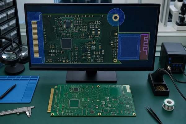
What Is a PCB Keepout Area and What Does It Restrict?
A PCB keepout area is an exclusion rule, not a physical layer that automatically appears on the finished board. Its boundary tells the layout system which objects may not enter a defined two-dimensional or three-dimensional space.
A complete keepout answers four questions: what is blocked, on which layers, within which boundary, and by which check. If any answer is missing, the drawing may look correct while traces, copper pours, vias, or package bodies remain unrestricted.
- Component restriction: blocks footprint placement where a connector must mate, a fastener needs access, or a moving part sweeps over the board.
- Routing restriction: prevents tracks from entering RF, isolation, board-edge, or mechanically exposed regions.
- Via and pad restriction: excludes drilled or plated features from contact surfaces, sealing areas, antenna fields, and mounting hardware.
- Copper restriction: removes planes, polygon pours, fills, or exposed copper while still permitting selected non-copper objects.
- Height restriction: reserves Z-axis volume above or below the PCB for an enclosure, heatsink, switch, cable, or connector body.
Match the restriction to the actual risk. An antenna may prohibit copper and vias on several layers, while a connector overhang may block only component bodies on one side. An unnecessarily broad rule consumes routing space and creates DRC violations that users may be tempted to waive.
PCB Keepout vs. Keepin, Clearance, Courtyard and Board Outline: What Is the Difference?
Choose the term by the relationship being controlled: a keepout excludes selected objects, a keepin confines them, clearance and creepage define spacing, a courtyard reserves assembly space, and the board outline or cutout defines manufactured geometry. The table below shows what each term controls and where it belongs in the design data.
| Terminology | Primary Function | Controlled Relationship | Technical Distinction |
| Keepout | Excludes selected objects from a region | Selected layout or mechanical objects | Available objects and layers depend on the EDA rule type |
| Keepin | Confines selected objects inside a region | Routing or component placement | Often used with the board boundary or functional blocks |
| Clearance | Maintains a minimum through-air distance | Spacing between conductive parts | Usually expressed as a rule value, not a drawn exclusion shape |
| Creepage | Maintains a minimum surface-path distance | Path between conductive parts along insulation | Must be calculated from the applicable safety requirements |
| Courtyard | Represents assembly and rework space around a footprint | Nearby component bodies and assembly access | It may be a reference boundary rather than an enforced rule |
| Board outline | Defines the finished board perimeter | Finished outer profile | It must not be replaced by a vague keepout boundary |
| Cutout or slot | Defines material that must be removed | Routed or drilled openings | It is a manufactured feature and requires explicit output data |
Use a keepout when the intent is “this object must not enter this region.” Use a clearance or creepage rule when a calculated minimum distance must be maintained. Use a courtyard for assembly spacing, and use an outline, slot, or cutout whenever laminate must be physically removed. Before release, verify that each requirement exists in the data type that can actually enforce or manufacture it.
What Types of PCB Keepout Areas Are Used in Layout?
PCB keepout types are classified by the objects they block and the physical risk they control. They are not interchangeable names for one universal layer. Select the narrowest rule that prevents the conflict without removing valid routing or placement space.
- Component keepout: prevents package bodies from entering connector mating zones, screw-tool access, ejector paths, fan openings, or moving switch envelopes. Verify it in placement DRC and the 3D assembly.
- Route keepout: blocks tracks in antenna fields, isolation barriers, sensitive analog regions, and areas vulnerable to milling or mechanical damage. Confirm whether the rule applies to one copper layer or every routing layer.
- Via keepout: prevents drilled features beneath seals, press-fit hardware, contact surfaces, flex-bend transitions, or restricted RF regions. Include the finished hole, pad, and fabrication tolerance when defining the boundary.
- Copper keepout: excludes planes, zones, fills, and sometimes pads around antennas, capacitive sensors, board edges, or exposed metalwork. Repour every zone before checking the result.
- Drill keepout: reserves space around slots, cavities, controlled-depth features, tooling locations, or thin webs that could break during routing. Confirm the rule against NC drill and rout data.
- Height keepout: defines the permitted Z-axis envelope above or below the PCB. Check component bodies, leads, solder, clips, cables, tolerances, and enclosure deflection rather than package height alone.
- Combined keepout: blocks several object classes when the same physical envelope controls them all. Use it only when the prohibited objects and affected layers truly share one boundary.
How Should a PCB Keepout Area Be Defined for Antennas, Mounting Holes, Connectors and Heatsinks?
Define each PCB keepout from the complete physical envelope, applicable tolerance, blocked object classes, and affected layers. Nominal body dimensions alone are insufficient because mating, fastening, airflow, cable movement, and enclosure variation can extend beyond the visible part.
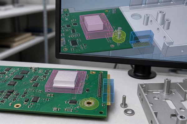
- PCB antenna keepout: start with the antenna or wireless-module reference layout. Copy the permitted board-edge position and restrictions for ground, signal copper, vias, components, shielding, batteries, displays, cables, and enclosure metal. Apply the rule to every specified layer, then confirm the final assembly rather than validating the bare board alone.
- Mounting-hole keepout: include the finished hole tolerance, pad or non-plated clearance, screw head, washer, standoff, locating boss, tool path, and expected board movement under torque. Keep copper only when the hardware is intentionally bonded to chassis or circuit ground.
- Connector keepout: model the receptacle, mating plug, latch, keying feature, insertion and removal path, cable bend radius, strain relief, and finger access. Check both populated and service positions, especially when the connector overhangs the board edge.
- Heatsink keepout: include the sink body, clips, screws, spring motion, insulation pad, mounting tolerance, airflow inlet and outlet, and neighboring component height. Add electrical clearance where the heatsink may be conductive or connected to a switching node.
- Board-edge keepout: account for finished-profile tolerance, router or V-score process, breakout tabs, edge plating, bevels, guide rails, enclosure grooves, and permitted component overhang. Keep the manufacturing profile separate from the placement or copper exclusion boundary.
For each zone, record the source dimension and revision, add the required positional tolerance, and run both DRC and a 3D collision check. If a requirement changes with a product variant, link it to the variant configuration instead of silently deleting the base constraint.
How Should a High-Voltage PCB Keepout Area Be Used with Creepage and Clearance Rules?
A high-voltage keepout can enforce an approved safety distance, but it cannot determine that distance. Clearance and creepage depend on the applicable product standard, working voltage, transient conditions, pollution degree, material group, altitude, coating, and insulation strategy.
- Identify the applicable product and safety requirements, insulation category, working and transient voltages, environment, altitude, and required protection level.
- Calculate clearance through air and creepage along the insulating surface separately. Do not reuse one value for both paths without a documented basis.
- Apply electrical clearance rules between the relevant nets or classes. Add object-specific keepouts where copper pours, vias, test pads, silkscreen, components, or conductive hardware must be excluded.
- Model slots and barriers as real routed or molded geometry. A keepout can reserve space for a slot, but it cannot create the slot in the fabricated board.
- Inspect the shortest path after routing, copper repour, component placement, coating definition, and mechanical assembly. Include conductive heatsinks, fasteners, connectors, and enclosure parts.
- Record the governing standard, revision, calculated values, assumptions, and any approved deviation in the released documentation.
Do not publish a universal keepout distance for “high voltage.” The correct value is application-specific. When altitude, coating, slots, or material classification changes, repeat the calculation and revalidate the physical path.
How Do Altium, KiCad, OrCAD and EasyEDA Represent PCB Keepout Zones?
In every PCB layout tool, verify which object classes the rule blocks and whether it applies to one layer or the full stackup. The commands and layer names differ, so confirm the following software-specific behavior before relying on an imported keepout.
- Altium Designer: object-specific keepouts may restrict vias, tracks, copper, SMD pads, and through-hole pads. A keepout on a signal layer acts only on that layer; a keepout on the Keep-Out Layer applies across signal layers. Keepout objects are design controls and are not normally emitted as Gerber or ODB++ artwork.
- KiCad: rule areas can exclude tracks, vias, pads, zone fills, and footprints on selected layers. Name critical areas so DRC messages identify the controlling zone, and repour zones after changes.
- OrCAD X: route keepouts, package keepouts, and keepins use different constraint subclasses. Confirm the subclass, side or layer scope, and whether the boundary controls etch, vias, or package placement.
- EasyEDA: copper exclusion and physical board openings use different solid-region or board-cutout functions. Rebuild copper and inspect the Gerber and drill/rout previews to confirm that an exclusion did not become an unintended cutout, or vice versa.
After migration between tools, select every critical zone and compare its name, boundary, restricted objects, side, layer span, and lock state with the source design. Then place a temporary prohibited object in the region, rerun DRC, repour copper, and inspect the manufacturing preview. A visible hatch pattern alone does not prove the rule survived translation.
How Do You Create and Verify a PCB Keepout Area with DRC?
Create the keepout from a controlled requirement, configure only the necessary restrictions, and prove its behavior with a deliberate DRC violation. A clean final DRC report is not enough if the rule was never shown to detect the condition it is meant to prevent.
- Define the hazard: state whether the zone controls RF performance, electrical isolation, component placement, service access, enclosure fit, routing damage, or a manufacturing process.
- Capture the source: obtain the controlling dimensions, tolerance, and revision from the datasheet, mechanical model, drawing, calculation, or compliance requirement.
- Select blocked objects: choose tracks, vias, pads, copper zones, components, drills, or height limits individually. Avoid an all-object rule unless every class is genuinely prohibited.
- Set the layer scope: apply the zone to the specific copper or component side, selected layers, or the full stackup as required. Confirm that the boundary is closed and includes positional tolerance.
- Assign ownership: place reusable constraints in the footprint or library when they must move with a component. Keep board-level and enclosure-level zones in the board design under revision control.
- Update dependent data: repour copper, update the design database, refresh 3D models, and run the complete electrical, placement, and mechanical rule set.
- Run a negative test: temporarily place each prohibited object class inside the zone. Confirm that DRC reports the correct rule name, location, and layer; then remove the test objects.
- Review released outputs: compare the final Gerber or intelligent data, NC drill/rout files, board profile, assembly drawing, and 3D model in independent viewers before release.
If a violation is intentionally accepted, record its location, technical reason, affected revision, approval, and expiration condition. Waive the single verified condition; do not disable the rule globally or suppress unrelated future errors.
Why Do PCB Keepout Area DRC Errors Occur and How Can They Be Fixed?
PCB keepout DRC errors usually come from an incorrect object restriction, layer scope, inherited footprint rule, stale copper pour, or translated geometry. Fix the rule definition or source geometry first; suppressing the message can leave the physical conflict in the released data.
- Footprint self-conflict: a library keepout overlaps the component’s own pads or body. Check whether the zone should exclude only neighboring components, vias, or copper. Correct the footprint rule and retest it in a sample board.
- Wrong-layer placement: an all-layer keepout was used when only the top or bottom surface required protection, or a local copper restriction was placed on the wrong layer. Move it to the intended layer and verify the remaining layers independently.
- Copper-pour anomaly: the zone was not repoured, its priority is wrong, or copper fills are not in the blocked-object list. Rebuild all zones and inspect both the DRC result and plotted copper.
- Imported-rule loss: translation converted the keepout into ordinary graphics or dropped its layer and object attributes. Recreate an enforceable rule in the destination tool and run a deliberate violation test.
- Boundary defect: an open contour, self-intersection, duplicate shape, or zero-width segment creates an unexpected result. Simplify the geometry, close the boundary, and check it at high zoom.
- Board-outline confusion: profile geometry was placed on a keepout or mechanical layer with an ambiguous name. Establish one authoritative closed outline and confirm it in the fabrication viewer.
Use a repeatable diagnosis order: read the violated rule, identify the offending object, inspect its layer, check whether the zone came from a footprint or the board, update copper, and reproduce the error with a test object. This isolates the cause before any waiver is considered.
What Common PCB Keepout Mistakes Cause Fabrication or Assembly Problems?
Most production problems occur when the drawn boundary does not match the restricted objects, required tolerance, 3D envelope, or released manufacturing data. Check the following failure modes before design release.
- Restricting everything: an unnecessary all-object or all-layer keepout blocks valid routing and encourages manual overrides. Limit it to the objects and layers connected to the actual risk.
- Ignoring tolerance: the boundary matches nominal CAD geometry but leaves no allowance for board profile, hole position, package size, fixture, or enclosure variation. Build the tolerance stack before fixing the boundary.
- Missing Z-axis space: the 2D layout passes while a heatsink, connector latch, cable, screw, solder fillet, or component lead collides in assembly. Validate top and bottom envelopes in the mechanical model.
- Using a keepout as a cutout: laminate remains because no routed geometry was supplied. Put slots and cutouts in the agreed fabrication and rout data, then verify them in CAM.
- Hiding requirements in notes: a text comment is not converted into an enforceable EDA rule, so later placement, routing, or copper changes bypass it. Use both an active rule and a clear drawing note where manufacturing visibility is needed.
- Sending ambiguous layers: files labeled GKO, GM1, Outline, or Mechanical may be interpreted differently. Map every nonstandard layer name in the README and identify one authoritative outline.
- Forgetting panel features: rails, tabs, mouse bites, V-scores, tooling holes, and fixture clamps can enter a board-level keepout after panelization. Review the production panel, not only the single-board layout.
Should PCB Keepout Areas Appear in Gerber, ODB++, IPC-2581 or Manufacturing Drawings?
Keepout rules do not normally need to become printed or etched artwork, but manufacturing-relevant constraints must be communicated unambiguously. Gerber primarily describes physical layer images; a keepout often appears only through its effect, such as missing copper or displaced features.
- Gerber: verify the effect of a copper keepout in each plotted copper layer. Do not expect a design-rule object to become a machine instruction unless a separate, clearly identified documentation layer is intentionally supplied.
- ODB++ or IPC-2581: use the richer product model when the receiving CAM system supports it, but confirm that keepout attributes, layer scope, component data, and profile geometry survive import.
- NC drill and rout data: provide every real hole, slot, cavity, cutout, or routed profile as physical manufacturing data. A reserved layout region cannot substitute for tool-path information.
- Fabrication drawing: identify the authoritative board profile, profile tolerance, copper-to-edge controls, special edge features, and any area that affects routing, plating, or panelization.
- Assembly drawing and 3D model: communicate component, connector, cable, fastener, tool-access, underside, and height exclusions that cannot be inferred from bare-board artwork.
Before release, overlay the copper, profile, drill, and rout outputs in an independent viewer. Then compare the intelligent data or drawing with the same revision of the PCB database. The acceptance question is not whether a file is named “keepout,” but whether every required physical result is visible and unambiguous.
How Should PCB Keepout Requirements Be Communicated to the Fabricator and Assembler?
Communicate the required physical result, controlling dimensions, tolerance, affected process, and authoritative source file. The word “keepout” alone does not identify whether copper, drilling, routing, placement, tooling, or Z-height is restricted.
- Fabrication package: provide Gerber or ODB++/IPC-2581, separate plated and non-plated drill data, one authoritative closed board outline, and clearly identified slots, cutouts, cavities, or controlled-depth features.
- Fabrication drawing: state finished dimensions, datum scheme, profile and hole tolerances, copper-to-edge controls, bevels, castellations, edge plating, and any panel-routing restriction.
- Assembly package: identify component-body, connector-mating, cable, fastener, heatsink, tooling, fixture, and top/bottom height exclusions. Include variant-dependent restrictions where fitted hardware changes the envelope.
- Mechanical model: provide STEP or an agreed ECAD/MCAD exchange format when enclosure fit, guide rails, mating parts, or moving hardware control the available space.
- README and revision record: map nonstandard layer names, identify the authoritative files, list deliberate omissions, and confirm that drawings, models, and manufacturing outputs share one revision.
When a manufacturer requests a “keepout layer,” confirm whether the request means the board outline, copper-to-edge clearance, panel-routing clearance, tooling exclusion, or assembly restriction. Resolve the meaning in writing before CAM edits begin, and record any approved data change in the release package.
What PCB Keepout Checks Should Be Completed Before Design Release?
Before design release, prove that every critical keepout is traceable, enforceable, dimensionally complete, visible in the correct output, and consistent with the mechanical assembly. Complete the checks after the last placement, routing, copper-pour, footprint, and enclosure update.
- Constraint source: trace every critical zone to a current datasheet, drawing, calculation, mechanical model, safety requirement, or approved manufacturing rule.
- Restriction scope: confirm the blocked objects, board side, affected layers, and whether the zone applies to routing, placement, copper, drilling, height, or several classes.
- Boundary and tolerance: check closed geometry, dimensions, datums, package and profile variation, assembly movement, and any added safety or service allowance.
- Library ownership: verify that component-specific zones move and rotate with the footprint, appear on the correct side after flipping, and do not create unintended self-conflicts.
- Electrical and RF review: repour copper and check antenna restrictions, return paths, isolation barriers, high-voltage spacing, shields, and conductive mechanical parts.
- Mechanical review: run top and bottom 3D collision checks for enclosures, connectors, cables, fasteners, heatsinks, guide rails, fixtures, and moving parts.
- DRC evidence: confirm each critical rule detects an intentional test violation, then remove test objects and close every remaining violation with a correction or documented waiver.
- Output review: overlay Gerber, drill, outline, slot, copper, assembly, and mechanical data in independent viewers and verify that all files share the released revision.
- Panel and process review: check rails, tabs, V-scores, tooling holes, fiducials, clamps, test probes, depanelization tools, and assembly access against board-level exclusions.
How Can Manufacturer DFM Review Verify PCB Keepout and Mechanical Constraints?
Manufacturer DFM should verify that the released geometry can be fabricated, panelized, assembled, and inspected without entering the defined exclusions. This review confirms production compatibility; it does not replace functional, RF, safety, or enclosure validation.
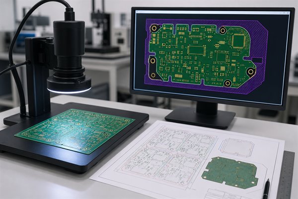
- Profile and routing: compare the authoritative outline with routed profiles, slots, cutouts, internal radii, bevels, edge plating, and dimensional tolerances.
- Copper and drilling: check copper-to-edge distance, holes and pads near cutouts, plated versus non-plated definitions, and any reserved area that affects drilling or copper removal.
- Panelization: place rails, breakaway tabs, mouse bites, V-scores, tooling holes, fiducials, and clamps without entering component, antenna, connector, or board-edge restrictions.
- Assembly access: check package overhang, bottom-side parts, connector mating space, fastener access, heatsink hardware, solder fixtures, test probes, and depanelization clearance.
- Data consistency: compare manufacturing data, drill/rout files, fabrication and assembly drawings, centroid data, BOM variants, and the mechanical model for revision or geometry conflicts.
- Exception control: report ambiguous layers and conflicting dimensions through a documented query. Do not move copper, alter profiles, or reinterpret a keepout without approval.
The review should return marked-up findings, affected coordinates or reference designators, proposed corrections, and a record of approved changes. Send final manufacturing outputs, stackup, drawings, mechanical model, panel preferences, and notes identifying critical keepouts. A PCB keepout area review is most effective before tooling, panelization, or placement data is frozen.
FAQs About PCB Keepout Areas
Q1: Does a keepout control the autorouter as well as manual routing?
A1: Only if the autorouter reads that rule type. Test-route through the region and confirm that the tool blocks it.
Q2: Can a PCB keepout area have an irregular or curved boundary?
A2: Yes. Use the simplest closed shape covering the restricted envelope. Extra vertices complicate editing and translation.
Q3: Do solder mask and paste layers need separate keepout rules?
A3: Usually, yes. Copper, solder mask, paste, and silkscreen are separate outputs. Define and plot each required exclusion.
Q4: How should imported vendor footprints with keepouts be checked?
A4: Compare it with the current datasheet, inspect every restricted object and layer, and trigger a test violation. Quiet DRC is not proof.
Q5: What happens to keepouts when a component is replaced?
A5: Recheck the body, mating path, thermal hardware, antenna rules, and Z-height. Pin compatibility does not prove mechanical compatibility.
Q6: Should test points have their own keepout area?
A6: Add one when a probe or fixture needs access. Cover the tool envelope and tolerance, not only the pad diameter.
Q7: How should keepouts be handled in PCB assembly variants?
A7: Keep common constraints in the base design. Document variant rules when optional hardware changes the occupied space.
Q8: Can panel rails, breakaway tabs, or V-scores violate board-level keepouts?
A8: Yes. Panelization adds temporary geometry. Check rails, tooling holes, fiducials, tabs, mouse bites, and V-scores.
Q9: Should a DNP component’s keepout be removed?
A9: Not automatically. Retain it for future population, service access, fixtures, or enclosure clearance. Remove it only through variant review.
Q10: How can ECAD and MCAD teams prevent keepout changes from being lost?
A10: Exchange revision-controlled models, assign each constraint owner, review changes, and rerun DRC plus collision checks.
If your design includes critical antenna, board-edge, mounting, connector, high-voltage, or enclosure restrictions, send the manufacturing package to EBest Circuit for DFM review. Email Gerber/ODB++, drill files, stackup, fabrication and assembly drawings, quantity, test requirements, and mechanical model to sales@bestpcbs.com for a technical review and quotation.
You may also like








Tags: PCB Keepout Design Rules, PCB Keepout DRC, PCB Keepout Layer, PCB Keepout Manufacturing Files