PCB manufacturing PCB manufacturing
Home > Blog

MCPCB Stackup: Select the Right Structure for Your Design

September 10th, 2026

An MCPCB stackup determines how heat leaves a component, how much current the circuit can carry, and how safely the copper remains isolated from the metal base. Selecting the stackup is therefore not a matter of choosing the highest thermal-conductivity material. It is a sequence of decisions about the heat path, electrical layers, dielectric, base metal, and cooling interface.

A useful starting rule is simple: use the least complex structure that meets the routing requirement, then improve the part of the thermal path that actually limits component temperature. This avoids paying for thicker metal, more layers, or a premium dielectric that does not address the real bottleneck.

MCPCB stackup
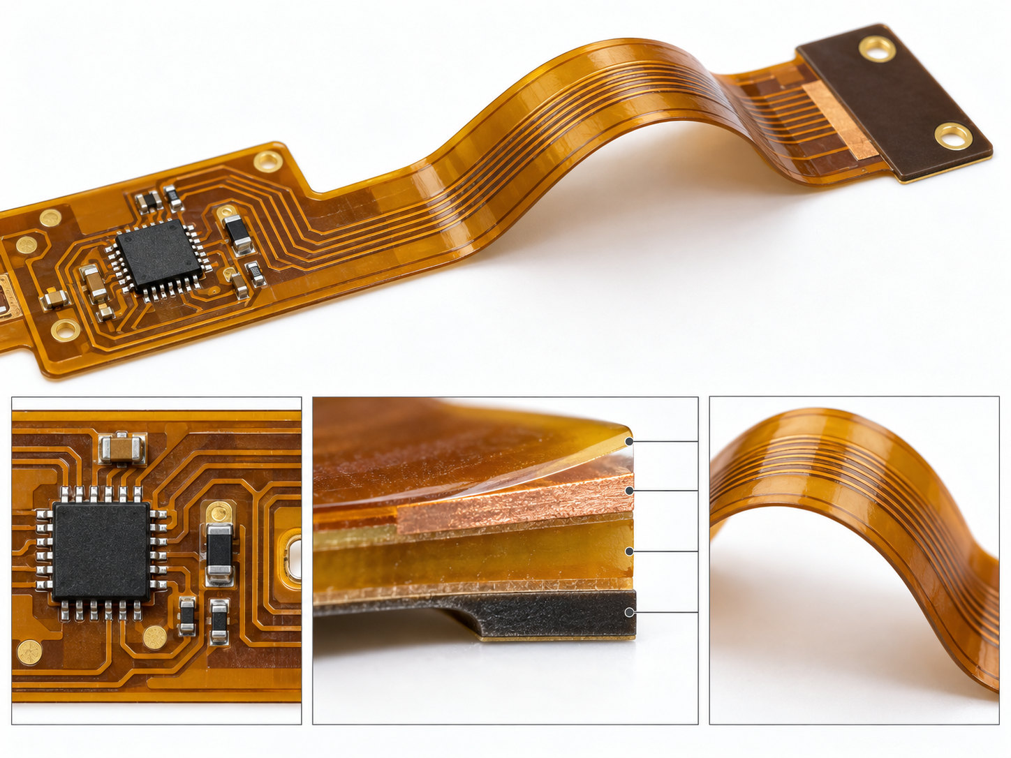
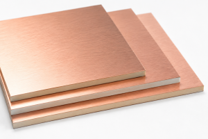
A thin MCPCB and a magnified view of its bonded copper, dielectric, and aluminum layers.

What Is an MCPCB Stackup?

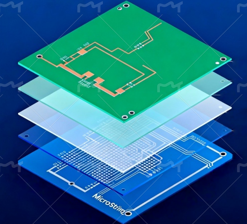
An MCPCB stackup is the cross-sectional order and thickness of the board’s conductive, insulating, and metal layers. A conventional single-layer MCPCB contains:

  • Copper circuit layer: forms traces and component pads and spreads heat laterally;
  • Thermally conductive dielectric: transfers heat downward while electrically isolating the copper;
  • Metal base: supports the board and spreads heat toward a heat sink, chassis, or enclosure.

These layers perform different jobs, so total board thickness alone does not define the design. A “1.5 mm aluminum PCB” could mean a 1.5 mm finished board or a 1.5 mm aluminum base plus copper and dielectric. It also says nothing about copper weight or dielectric thickness.

The stackup must be read as a complete heat path. Copper helps heat spread away from a small component pad. The dielectric controls much of the vertical resistance inside a conventional MCPCB. The metal base distributes heat over a wider area. The external cooling surface then removes that heat from the product.

This distinction explains why two boards with the same size and finished thickness can run at different temperatures. Their copper distribution, dielectric resistance, base material, or contact with the heat sink may be different.

How Does a Metal Core PCB Stackup Transfer Heat?

In a conventional metal core PCB stackup, heat normally travels through:

Component junction → package → solder or thermal pad → copper → dielectric → metal base → cooling interface → ambient air

Each stage adds thermal resistance. For a first-pass temperature estimate:

Temperature rise = Power × Total thermal resistance

If a device dissipates 10 W and the complete junction-to-ambient path is 4 °C/W, the expected temperature rise is approximately 40 °C above ambient. Reducing only the PCB dielectric resistance from 0.5 to 0.3 °C/W would lower that estimate by about 2 °C, not 20 °C. This prevents overestimating the benefit of one material upgrade.

Temperature measurements can help identify where the restriction lies:

  • Hot component, much cooler metal base: resistance is likely concentrated near the package, pad, copper spreading area, or dielectric.
  • Hot component and hot metal base, cooler heat sink: inspect the board-to-heat-sink interface.
  • Component, base, and heat sink all hot: the external cooling system cannot reject enough heat.
  • One local hotspot on an otherwise cool board: improve the local pad, copper spreading, or direct heat path before upgrading the whole board.

The decision is therefore not “Which metal conducts heat best?” It is “Which part of the junction-to-ambient path contributes enough resistance that changing it will materially lower temperature?”

MCPCB stackup
Heat moves through the thin MCPCB layers into the thermal interface and heat sink.

Which MCPCB Structure Fits Your Application?

Choose the layer structure from the circuit requirement first, then verify that its heat path is short enough for the hottest components.

Use a single-layer MCPCB when all components and routing fit on one copper layer. It offers the shortest conventional path from the component pad through one dielectric layer to the metal base. This is often suitable for LED arrays, power modules, motor drives, and simple high-current circuits.

Move to a double-layer MCPCB when one layer cannot provide the required routing, ground plane, power distribution, or connector access. The second copper layer earns its place by solving an electrical problem. Heat from the upper layer may travel through vias or additional dielectric before reaching the base, so it is usually less direct.

Use a multilayer MCPCB when routing density, signal separation, power planes, or component placement requires more than two copper layers. Do not select it only because power is high; extra layers can increase rather than reduce the distance to the metal base.

A practical decision sequence is:

  1. Place the components and identify the devices that dominate heat generation.
  2. Check whether one copper layer can meet routing and current requirements.
  3. Add another layer only when a defined electrical constraint cannot be solved cleanly.
  4. Trace the heat path from each critical device to the metal base.
  5. If only one area has excessive heat density, compare a localized solution with increasing the complexity of the entire board.

For example, a 100 W LED assembly distributed across a large board may work well on a single-layer aluminum MCPCB. A 40 W power-control board with dense gate-drive and sensing circuits may require two or more copper layers even though its total power is lower. Total wattage alone does not determine the layer count.

MCPCB stackup
Identical thin LED boards with aluminum and copper metal bases.

How Do Aluminum and Copper Bases Affect Performance?

Choose aluminum when the base provides adequate heat spreading and weight or cost matters. Choose copper when heat is concentrated in a small area and spreading through the base is a significant part of the temperature rise.

Copper’s thermal conductivity is roughly higher than aluminum’s, so it can reduce temperature differences across the metal base. The benefit is greatest when heat must spread laterally from a small source before reaching a larger heat sink. It is smaller when heat already enters a large area or when the dielectric and external interface dominate total resistance.

Use these observations:

  • Several devices create a hotspot near the center while the base edges remain cool: copper may improve lateral spreading.
  • The whole aluminum base is nearly uniform but too hot: changing to copper is unlikely to solve insufficient external cooling.
  • The component is hot while the aluminum directly beneath it is much cooler: improve the path through the pad, copper, or dielectric first.
  • Product weight and material cost are sensitive: aluminum is normally the better starting point.

Base thickness follows a similar rule. Increasing thickness improves stiffness and gives heat more cross-sectional area for lateral spreading. It does not reduce the dielectric resistance, and it does not create additional cooling capacity. Once the base temperature is reasonably uniform, making it thicker usually produces diminishing thermal returns.

The choice should therefore be based on measured or modeled temperature distribution, not on the assumption that copper or a thicker base is automatically safer.

How Should You Select the Dielectric Layer?

Select the dielectric by setting an allowable thermal resistance first, then checking that the chosen thickness provides sufficient electrical isolation and reliability.

The approximate thermal resistance of the dielectric is:

Rθ = t ÷ (k × A)

where:

  • t is dielectric thickness in meters;
  • k is thermal conductivity in W/m·K;
  • A is effective heat-transfer area in square meters.

Assume an effective area of 100 mm²:

  • 100 μm at 3 W/m·K gives approximately 0.33 K/W;
  • 75 μm at 2 W/m·K gives approximately 0.38 K/W.

Although the first material has 50% higher conductivity, its calculated layer resistance is only slightly lower because it is also thicker. This is why comparing W/m·K alone can be misleading. The calculation is illustrative and excludes package, solder, copper-spreading, contact, and heat-sink resistance.

Use this selection order:

  1. Estimate how much of the total temperature rise can be allocated to the dielectric.
  2. Compare candidate materials using conductivity, actual thickness, and effective pad area.
  3. Eliminate options that do not provide adequate isolation for operating voltage, transients, tolerances, and environment.
  4. Check adhesion, soldering exposure, thermal cycling, moisture, and aging requirements.
  5. Confirm with thermal modeling or a prototype only when the remaining margin is too small for a first-order estimate.

The correct action depends on the bottleneck:

  • If dielectric resistance is too high but isolation margin is generous, reducing thickness may be effective.
  • If thickness cannot be reduced safely, use a higher-conductivity dielectric or increase the heat-transfer area.
  • If the entire metal base is already hot, improving the dielectric will have limited value; improve the external cooling path.
  • If one small pad is hot, enlarge the copper area or use a localized thermal structure before upgrading the dielectric across the whole board.
MCPCB stackup
Tightly bonded single-layer, double-layer, and multilayer MCPCB cross-sections.

When Do You Need a Double Layer MCPCB or Multilayer MCPCB?

A Double Layer MCPCB is justified when the second copper layer solves a specific electrical-layout problem. A Multilayer MCPCB is justified when additional routing layers or planes are necessary. The thermal design must then be adapted to the longer and more complex path.

Consider a component on the top copper of a two-layer construction. Its heat may spread in the top copper, move through thermal vias to a lower copper layer, cross the dielectric, and enter the metal base. The vias reduce part of the vertical resistance, but they do not make the path identical to a single-layer MCPCB.

The layer choice changes these factors:

  • Routing capacity: improves as copper layers are added.
  • Vertical heat distance: may increase when more dielectric separates the component from the metal.
  • Via dependence: increases when heat and current must move between layers.
  • Copper balance: becomes more important for flatness and consistent heat spreading.
  • Thickness and mass: generally increase with additional layers.

If the circuit needs only one or two local crossovers, redesigning the routing may be better than adding a complete layer. If a dense control circuit requires planes and signal separation across the board, the extra layers have clear value.

When one or two devices dominate the heat load, keep the required electrical layers but compare local thermal vias, direct thermal path, copper inserts, or ceramic beneath those devices. This separates the routing problem from the hotspot problem instead of forcing one structure to solve both inefficiently.

Which Stackup Details Should Your Fabrication Drawing Define?

The drawing should show enough cross-sectional information to distinguish the intended MCPCB from every plausible alternative.

At minimum, show:

  • each copper layer and its finished thickness;
  • each dielectric layer and its thickness;
  • metal type and metal-base thickness;
  • total finished board thickness;
  • the position of the metal relative to all copper layers;
  • vias, insulated holes, exposed metal, or direct thermal features that change the heat path.

Avoid one-line descriptions that combine several dimensions. Instead of “1.5 mm aluminum PCB, 2 oz copper,” separate the structure:

70 μm finished copper / 100 μm dielectric / 1.5 mm aluminum base

This shows immediately that the base is 1.5 mm and the total finished board will be thicker. If 1.5 mm is intended as the overall thickness, the base must be adjusted accordingly.

For multilayer structures, draw each copper and dielectric layer in order and show which vias connect them. If a hole passes through the metal, show the insulating clearance around it. If a component uses a direct thermal path, show where the thermal pad contacts metal and where electrical isolation remains.

Also separate material properties from product targets. A dielectric conductivity value defines one layer. A maximum component temperature under a stated power and cooling condition defines the expected outcome. Both are useful, but neither can substitute for the other.

How Do Stackup Choices Affect Cost and Lead Time?

Stackup cost and lead time rise when a choice adds expensive material, less available material, or additional processing steps. The largest increase usually comes from combinations of changes rather than one specification alone.

The direction of each effect is predictable:

  • Aluminum to copper: raises material cost and weight; the benefit is strongest for concentrated heat spreading.
  • Standard to uncommon dielectric: may add sourcing time; use it when the thermal or insulation margin requires it.
  • Standard to heavy copper: increases imaging and etching difficulty and may require wider spacing.
  • Single layer to multilayer: adds lamination, drilling, plating, and alignment operations.
  • Conventional to direct thermal path or copper insert: adds localized processing but may solve a hotspot that bulk material upgrades cannot.
  • Common to tightly controlled thickness: reduces the available material and process window.

Use a value-based comparison rather than selecting the lowest board price. Suppose a copper base adds cost but lowers the critical device temperature by only 1 °C because the dielectric is the main resistance. That upgrade has poor value. If the same change lowers a concentrated hotspot enough to remove a larger heat sink, it may reduce total product cost.

Lead time follows material and process readiness. A common single-layer aluminum stackup has fewer dependencies. A multilayer copper-base construction with a special dielectric, heavy copper, and insulated metal-core holes combines several dependencies and will usually take longer.

The best-value stackup is the least complex one that meets the electrical limits and thermal target without paying for improvements outside the real bottleneck.

FAQs About MCPCB Stackup

Is every metal core PCB an aluminum PCB?

No. Aluminum is the most common base, but copper and specialized metal structures are also used. The choice depends on heat concentration, weight, cost, and the external cooling design.

Does higher dielectric conductivity always make the board cooler?

No. Actual layer resistance also depends on dielectric thickness and effective heat-transfer area. Package, solder, copper spreading, base metal, and cooling-interface resistance may dominate the result.

Does a thicker metal base always improve cooling?

No. It improves stiffness and lateral heat spreading, but it cannot compensate for a restrictive dielectric or inadequate external cooling. Once the base temperature is nearly uniform, additional thickness gives diminishing thermal benefit.

When is copper better than aluminum?

Copper is most useful when heat is concentrated and temperature varies significantly across the metal base. If the entire base is already uniformly hot, the external cooling system is the more likely limitation.

Can thermal vias improve an MCPCB stackup?

Yes, in double-layer and multilayer structures. They can connect copper areas and shorten part of the vertical path. Their effect depends on quantity, diameter, copper plating, placement, and the remaining dielectric-to-metal path.

Can one stackup support different power levels?

Yes. Power is only one input. Heat-source area, duty cycle, ambient temperature, airflow, enclosure, cooling contact, and allowable component temperature also determine whether the stackup works.

Need help comparing two MCPCB stackup options? Send the cross-sections, power dissipation, voltage, thermal target, and cooling conditions to sales@bestpcbs.com.

You may also like

Current Sensors: Types, Working Principle, Applications & Selection Guide

September 10th, 2026
Current sensors measure the current flowing through a conductor and convert it into a signal for monitoring, control, protection, or power calculation. Common sensing methods include shunt resistors, Hall effect sensors, current transformers, Rogowski coils, and fluxgate sensors. Some measure both AC and DC, while others are designed mainly for AC.

Choosing the right current sensor depends on more than the ampere range. Engineers also need to consider isolation, accuracy, bandwidth, response time, temperature drift, insertion loss, and PCB layout. These factors determine whether the sensor performs as expected once it is integrated into the final circuit.

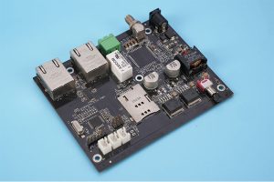
Current sensors on a PCB and electronics test setup

What Is a Current Sensor and What Does It Measure?

A current sensor detects the magnitude, and sometimes the direction, of current flowing through a conductor.

The measured current is converted into an electrical signal that can be read by a controller, ADC, protection circuit, or monitoring system. Depending on the sensor, the output may be analog, digital, current-based, or frequency-based.

Current sensors are commonly used for:

  • Overcurrent protection
  • Battery charge and discharge monitoring
  • Motor current control
  • Power measurement
  • Load detection
  • Power supply regulation
  • Fault monitoring

A current sensor measures current, while a voltage sensor measures the potential difference between two points. In power-monitoring systems, both are often used together.

How Do Current Sensors Work?

Current sensors work by measuring either the voltage produced by current flow or the magnetic field created around the conductor.

Direct shunt sensing and magnetic current sensing methods

There are two basic sensing approaches.

Direct sensing

A low-value resistor is placed in series with the current path. The voltage across it follows Ohm’s law:

V = I × R

The circuit measures this voltage and calculates the current.

This approach is simple and accurate, but the resistor creates some power loss:

P = I²R

That loss becomes more important as current increases.

Magnetic sensing

Current flowing through a conductor creates a magnetic field. A magnetic current sensor detects this field without relying on a measurable voltage drop across a series resistor.

Common magnetic sensing methods include:

  • Hall effect sensing
  • Current transformers
  • Rogowski coils
  • Fluxgate sensing
  • Magnetoresistive sensing

The sensing principle determines whether the device can measure AC, DC, or both.

What Are the Main Types of Current Sensors?

The main types of current sensors are shunt resistors, Hall effect sensors, current transformers, Rogowski coils, and fluxgate sensors.

Five main types of current sensors including shunt, Hall effect, current transformer, Rogowski coil and fluxgate
Current Sensor Type AC DC Isolation Main Advantage Main Limitation
Shunt resistor Yes Yes No inherent isolation Accurate and simple Power loss
Hall effect sensor Yes Yes Available AC/DC sensing with isolation Offset and temperature drift
Current transformer Yes No Yes Efficient AC sensing Cannot measure steady DC
Rogowski coil Yes No Yes Handles very high AC current Requires signal integration
Fluxgate sensor Yes Yes Yes High DC accuracy Higher cost and complexity

Shunt resistor

A precision resistor creates a small voltage proportional to current. It is widely used in battery circuits, power supplies, and low-voltage power electronics.

Hall effect sensor

A Hall sensor measures the magnetic field around the conductor. It is widely used where AC/DC measurement and isolation are both required.

Current transformer

A current transformer reproduces AC current in a secondary winding. It is common in power monitoring, protection, and mains-connected equipment.

Rogowski coil

A Rogowski coil measures changing current without using a conventional magnetic core. It is well suited to high AC currents and fast current waveforms.

Fluxgate sensor

Fluxgate sensing is used when low offset, good linearity, and accurate DC measurement are important.

The correct type depends mainly on current waveform, isolation needs, accuracy, bandwidth, and current range.

How Do Hall Effect Current Sensors Work?

Hall effect current sensors measure the magnetic field generated by current flowing through a conductor.

Hall effect current sensor working principle with magnetic field and output signal

As current passes through the conductor, a magnetic field forms around it. A Hall element detects this field and produces a signal related to the magnetic flux density. Internal circuitry then amplifies and conditions the signal into a usable current measurement.

Hall sensors are commonly divided into two architectures.

Open-loop Hall sensors

These measure the magnetic field directly. They are relatively simple, compact, and cost-effective.

Closed-loop Hall sensors

These generate a compensation current that opposes the magnetic field from the primary conductor. The compensation current is then used as the measurement signal.

Closed-loop designs can provide better:

  • Linearity
  • Accuracy
  • Response time
  • Temperature stability

Hall effect current sensors can measure both AC and DC because the Hall element responds directly to magnetic field strength.

Integrated Hall current sensor ICs are widely used in PCB-mounted designs because the sensing element, signal conditioning, and current path can be combined in one package.

Which Current Sensors Can Measure DC Current?

Shunt resistors, Hall effect sensors, fluxgate sensors, and magnetoresistive sensors can measure DC current. Standard current transformers and Rogowski coils cannot measure steady DC.

Sensor Type DC AC
Shunt resistor Yes Yes
Hall effect sensor Yes Yes
Fluxgate sensor Yes Yes
Magnetoresistive sensor Yes Yes
Current transformer No Yes
Rogowski coil No Yes

For DC current sensing:

  • Shunt resistors are simple and accurate but introduce resistance and heat.
  • Hall effect sensors are useful when isolation and higher-current capability are required.
  • Fluxgate sensors suit precision DC measurement where low offset and drift matter.

Current transformers cannot measure steady DC because they rely on changing magnetic flux. Rogowski coils have the same basic limitation and are therefore used for AC or transient current measurement.

What Specifications Matter When Choosing a Current Sensor?

The most important current sensor specifications are current range, AC/DC capability, accuracy, bandwidth, isolation, temperature drift, and output type.

The main parameters to check are:

  • Current range: Include nominal current, peak current, startup current, and possible fault current.
  • AC or DC capability: Confirm that the sensing principle supports the required waveform.
  • Bidirectional sensing: Battery and regenerative systems often need positive and negative current measurement.
  • Accuracy: Consider gain error, offset, nonlinearity, and noise.
  • Bandwidth: Higher bandwidth is needed for switching converters, inverters, and fast control loops.
  • Response time: Protection circuits may need very fast current detection.
  • Isolation voltage: Check this carefully in high-voltage or mains-connected circuits.
  • Temperature drift: Offset and sensitivity may change as temperature rises.
  • Insertion loss: Shunt-based methods add resistance to the current path.
  • Output type: Analog voltage, current output, PWM, SPI, I²C, and other interfaces are available.
  • Package size: The package must suit the required current, thermal load, and PCB spacing.

A sensor with a suitable current range is not automatically the right choice. The total measurement error across temperature and operating conditions matters just as much.

Where Are Current Sensors Used?

Current sensors are widely used in systems that need to measure, control, or protect electrical power.

Current sensor applications in battery systems, motor drives, inverters, EV chargers and industrial controls

Typical applications include:

  • Battery management systems: Measure charge and discharge current and support overcurrent protection.
  • Motor drives: Monitor phase current for torque control, feedback, and fault protection.
  • Power supplies: Support current regulation, current limiting, and output monitoring.
  • Solar inverters: Measure current on DC input stages, conversion stages, or AC output.
  • Energy storage systems: Track bidirectional battery current during charging and discharging.
  • Industrial equipment: Detect overloads, abnormal loads, and changes in machine operation.
  • EV charging systems: Monitor power conversion and charging current.

Different current sensors may be used within the same product because low-current control circuits and high-current power stages often have different requirements.

How Does PCB Design Affect Current Sensor Accuracy?

PCB layout can directly affect current sensor accuracy through trace resistance, heat, magnetic interference, grounding, and signal routing.

Current sensor PCB layout with Kelvin sense traces, high-current copper path and isolation spacing

For shunt-based current sensing, Kelvin connections are especially important. The sense traces should measure voltage directly across the shunt rather than including voltage drops from the high-current copper path.

Good shunt layout usually includes:

  • Separate Kelvin sense traces
  • Short differential routing to the amplifier
  • Minimal coupling from switching nodes
  • Controlled high-current copper paths
  • Careful ground routing
  • Limited temperature gradients around the shunt

Hall effect sensors have a different set of layout concerns.

Nearby magnetic fields from components such as these can distort the measurement:

  • Inductors
  • Transformers
  • Busbars
  • High-current PCB traces
  • Adjacent power conductors

For isolated current sensors, PCB creepage and clearance must also be maintained around the isolation barrier. Vias, copper pours, test pads, and nearby components should not reduce the intended spacing.

How Do You Choose the Right Current Sensor for Your Circuit?

Choose a current sensor by matching the sensing technology to the current waveform, isolation requirement, current range, accuracy, and response speed.

A practical selection process starts with five questions.

1. Do you need AC, DC, or both?

For DC or bidirectional current, common options include:

  • Shunt resistor
  • Hall effect sensor
  • Fluxgate sensor
  • Magnetoresistive sensor

For AC-only measurement, current transformers and Rogowski coils are also available.

2. Do you need galvanic isolation?

If the control circuit must be electrically separated from the power path, isolated Hall, current transformer, Rogowski, or fluxgate solutions are more suitable.

3. What is the maximum current?

Do not design around nominal current alone. Include:

  • Startup current
  • Motor stall current
  • Regenerative current
  • Switching peaks
  • Fault current

4. How much accuracy and bandwidth are required?

Energy metering, battery monitoring, motor control, and overcurrent protection all have different measurement requirements.

5. Can the PCB support the sensor properly?

Check:

  • Current-carrying copper
  • Thermal rise
  • Isolation spacing
  • Magnetic interference
  • Shunt routing
  • Package footprint

A useful starting comparison is:

Requirement Common Starting Point
Low-cost AC/DC sensing Shunt resistor
Isolated AC/DC sensing Hall effect sensor
High-current AC sensing Current transformer
Very high AC current Rogowski coil
Precision isolated DC sensing Fluxgate sensor
Compact PCB-level sensing Integrated current sensor IC

The final choice should meet the complete system requirement rather than simply matching the current rating.

FAQ About Current Sensors

1. What are the main types of current sensors?

The main types are shunt resistors, Hall effect sensors, current transformers, Rogowski coils, and fluxgate sensors. They differ in AC/DC capability, isolation, accuracy, bandwidth, and current range.

2. Can a current sensor measure both AC and DC?

Yes. Hall effect, shunt, fluxgate, and magnetoresistive sensors can measure both AC and DC. Standard current transformers and Rogowski coils cannot measure steady DC.

3. What is a Hall effect current sensor?

A Hall effect current sensor measures the magnetic field generated by current flowing through a conductor. It can measure AC and DC and can provide galvanic isolation.

4. What is the difference between a current sensor and a current transformer?

A current transformer is one type of current sensor used mainly for AC measurement. Current sensor is a broader term that also includes Hall, shunt, Rogowski, fluxgate, and other sensing methods.

5. What is the difference between a current sensor and a voltage sensor?

A current sensor measures current flowing through a conductor. A voltage sensor measures the electrical potential difference between two points.

6. Can current sensors be used with Arduino?

Yes. Current sensors with a compatible analog or digital output can connect to Arduino boards. Check the sensor’s supply voltage, output range, interface, and maximum current before use.

Ready to Review Your Current-Sensing PCB or PCBA?

Current sensor performance can be affected by high-current routing, Kelvin connections, copper thickness, isolation spacing, heat, and component placement. These details are easier to correct during PCB review than after assembly.

EBest Circuit supports PCB fabrication and PCBA for battery systems, motor drives, industrial controls, power supplies, chargers, and other current-sensing applications. Send your Gerber files, BOM, stackup, current requirements, and assembly specifications to sales@bestpcbs.com for DFM and manufacturing review.

You may also like

Rigid Flex PCB Manufacturer Germany: Top 5 Suppliers to Compare

September 10th, 2026

Choosing a rigid-flex PCB manufacturer in Germany involves more than finding a supplier that offers flexible circuits. Your board may need several rigid sections, a thin flexible connection, controlled impedance or HDI routing within a compact enclosure. The useful comparison is which manufacturers can produce that construction—and which production route suits your project.

EBest Circuit offers an overseas manufacturing option for German customers, with experience manufacturing a 10-layer rigid-flex PCB for a German medical product. That project combined adhesiveless polyimide, impedance requirements, resin-plugged holes and drawing-specific stainless steel stiffeners. Alongside PCB fabrication, EBest provides DFM review, component sourcing and assembly support. Send your requirements to sales@bestpcbs.com to discuss your project, or arrange a visit to our factory in China to meet the team and review our manufacturing capabilities.

rigid flex PCB manufacturer Germany

Rigid Flex PCB Manufacturer Germany: 5 Suppliers Compared

These five manufacturers offer rigid-flex PCB production in Germany. The comparison below focuses on their main business, relevant strengths and manufacturing capabilities. The five companies are compared by their capabilities, without ranking them from best to worst.

1. Würth Elektronik (Germany)

  • Main Business: PCB manufacturing, including rigid-flex circuits for compact electronic assemblies.
  • Advantages: Defined stackup options, physical technology samples and development-stage guidance help customers compare rigid-flex constructions before finalising a design.
  • Production Capability: Its rigid-flex technology range includes FR4/polyimide constructions with internal or external flex layers, plus HDI microvia combinations for dense component routing.

2. KSG (Germany; additional production in Austria)

  • Main Business: Rigid-flex PCB manufacturing from design development through series production at its own European facilities.
  • Advantages: Technical support for stackup and layout review, with optional edge sealing to reinforce demanding rigid-to-flex transitions.
  • Production Capability: Its rigid-flex manufacturing capabilities include 2–18 layers, FR4/polyimide materials, symmetric and asymmetric constructions, and HDI compatibility. Available combinations depend on the board design.

3. CONTAG (Berlin, Germany)

  • Main Business: High-technology PCB fabrication, including rigid-flex boards and prototype production in Berlin.
  • Advantages: A broad choice of flex-section arrangements makes CONTAG relevant for designs that need several flexible layers or complex folding geometry.
  • Production Capability: Its rigid-flex manufacturing capabilities include internal and external flex layers, multilayer flexible sections, bookbinder constructions and HDI/SBU combinations.

4. ILFA (Hannover, Germany)

  • Main Business: Complex PCB manufacturing, with rigid-flex as a core technology.
  • Advantages: Dedicated rigid-flex design rules and experience with mixed-material constructions support projects that need a customised stackup.
  • Production Capability: Its rigid-flex technology combines FR4 cores with one or more polyimide flex cores, bonded using low-flow or no-flow prepregs. ILFA also offers HDI manufacturing; the combination required for an individual rigid-flex design needs technical review.

5. ANDUS ELECTRONIC (Berlin, Germany)

  • Main Business: PCB fabrication and electronic assembly, including flexible and rigid-flex circuits.
  • Advantages: In-house assembly and the integrated alpha-board design team offer a coordinated route from PCB layout to manufactured assemblies.
  • Production Capability: Its manufacturing capabilities include rigid-flex, complex multilayer boards, HDI and impedance measurement, alongside in-house assembly. Rigid-flex layer limits and process combinations should be confirmed for the proposed design.

Rigid-flex PCB stackup: What Can German Manufacturers Produce?

German manufacturers offer rigid-flex constructions with external flex layers, internal flex layers and multilayer flexible sections. The right choice depends on how the board fits inside the product, how many connections pass through the flexible section and whether it bends during installation or repeatedly in use.

External flex layers sit toward the outside of the rigid stack. The exposed flexible section connects the rigid board areas. Würth Elektronik and CONTAG offer this type of construction.

Internal flex layers run through the inside of the rigid sections and emerge between them. Würth Elektronik and CONTAG also support this arrangement, allowing the flexible connection to be incorporated within a multilayer rigid structure.

Multilayer flexible sections accommodate additional routing within the flex area. For more complex folding arrangements, CONTAG offers separated flex layers and bookbinder constructions, in which the flexible layers can follow different bend paths.

KSG offers 2–18-layer rigid-flex constructions, depending on the configuration, including symmetric and asymmetric stackups. The overall layer count must be distinguished from the number of layers in the flexible section: a 10-layer board can have fewer copper layers passing through the bend area.

For a compact medical product, the stackup needs to satisfy both the electrical design and the available space. Flex thickness, copper distribution and the rigid-to-flex transition affect how the board can be folded. A connection bent once during installation requires a different assessment from one that moves repeatedly throughout the product’s life.

Our guide to the rigid-flex PCB manufacturing process explains how the rigid and flexible sections are fabricated and joined into one board.

rigid flex PCB manufacturer Germany

Which German Suppliers Offer HDI Rigid-Flex PCBs?

Würth Elektronik, KSG and CONTAG offer rigid-flex constructions that can incorporate HDI technology. Their capabilities provide different starting points for boards that need dense routing alongside flexible connections.

Manufacturer HDI rigid-flex capability Relevance to your design
Würth Elektronik Rigid-flex combined with HDI microvias Fine-pitch component routing in compact rigid sections
KSG HDI-compatible rigid-flex stackups Projects requiring a coordinated choice of layer structure and interconnect technology
CONTAG HDI/SBU combinations and advanced via arrangements Complex build-up structures combined with flexible interconnections

When does HDI help? A densely connected BGA or a small rigid section may need microvias to route signals that conventional through-holes cannot accommodate within the available space. The selected via structure must work with the board’s materials and lamination sequence.

Does a 10-layer rigid-flex board automatically need HDI? No. Layer count and interconnect technology are separate design choices. A 10-layer board may use conventional plated through-holes, while a board with fewer layers may need microvias. Impedance control and resin plugging alone do not make a board an HDI design.

What Certifications Are Needed for Rigid-Flex PCB Projects for German Customers?

The relevant certifications depend on the product’s application and the customer’s supplier requirements. There is no single certification package that applies to every rigid-flex PCB purchased by a German company.

Certification Relevant project context
ISO 9001 General quality management
ISO 13485 Medical-device supply chains
IATF 16949 Automotive supply chains
AS/EN 9100 Aviation, space and defence supply chains

For medical projects, ISO 13485 is particularly relevant because it addresses quality management for medical devices and related services. However, a supplier’s certificate does not by itself approve the finished medical product. The certificate’s scope, covered site and validity must match the work being purchased.

Automotive customers may specify IATF 16949, while aerospace programmes may require a quality system based on 9100. These are application-specific considerations, not universal requirements for German PCB orders.

Board acceptance requirements are a separate matter. The purchase specification can identify the agreed revision and performance class of IPC-6013 for flexible and rigid-flex printed boards. Relevant material compliance documentation, such as RoHS, also serves a different purpose from a quality management certificate.

EBest’s quality certifications include ISO 9001:2015, ISO 13485:2016, IATF 16949 and AS9100D. For a specific project, request the current certificate and applicable scope as part of supplier qualification.

What Lead Times Can EBest Circuit Offer for Rigid-Flex PCB Projects in Germany?

EBest’s rigid-flex production lead times provide a starting point for scheduling:

Rigid-flex construction Normal service Fastest service
4 layers 2 weeks 1.5 weeks
More than 4 layers Project-specific Project-specific

For a 10-layer board, the schedule requires a separate quotation. The four-layer timing should not be carried over to a multilayer medical project with resin plugging, impedance requirements and stainless steel stiffeners.

Production time and arrival in Germany are different milestones. Freight and customs arrangements must be added to the factory schedule. Your required arrival date should therefore be included in the enquiry, alongside the board specification and quantity.

For urgent projects, share your target delivery date when you enquire. EBest can assess the production time for your board and discuss whether an expedited schedule is available.

EBest also provides online WIP updates for production progress. For a German customer coordinating assembly or product builds, that visibility helps connect the factory schedule with the next operation. The order-specific dispatch date and shipping arrangement should be recorded in the quotation or order confirmation.

Case Study: Rigid-Flex PCB Manufacturing for a German Customer

EBest Circuit manufactured a 10-layer rigid-flex PCB for a German customer’s medical product. The design combined a multilayer rigid structure with a thin flexible section and local stainless steel reinforcement.

Project feature Specified requirement
Board construction 10-layer rigid-flex; FR4 Tg170 and adhesiveless PI
Overall thickness 1.2 mm ±0.1 mm
Flexible section 0.23 mm thickness
Hole treatment 25 µm PTH copper; resin plugging
Local reinforcement 0.2 mm SUS304 at drawing-defined locations
Electrical requirement Controlled impedance

Two thickness requirements shaped the construction. The overall board thickness and the much thinner flexible section describe different parts of the same board. They need to be considered together so that the rigid sections fit the product while the flexible connection can follow the intended mechanical path.

The impedance requirement made material and copper selection electrically significant. The project specified 3 mil adhesiveless polyimide, 1 oz outer copper and 0.5 oz inner copper. Those inputs form part of the stackup used to determine impedance geometry, connecting the material specification directly to the electrical design.

Resin plugging and stainless steel reinforcement added drawing-specific manufacturing work. Resin plugging was an explicit hole-treatment requirement. The SUS304 stiffeners had specified positions and a defined thickness, making their placement part of the mechanical design rather than an interchangeable finishing option.

For a similar medical product, this combination is more informative than a layer count alone: the manufacturer must accommodate the thin flexible section, controlled electrical structure and local mechanical reinforcement within one board.

Why Choose EBest Circuit for Your Rigid-Flex PCB Project in Germany?

EBest is a manufacturing option in China for German customers seeking support with a defined rigid-flex design. The strongest reason to consider us is the fit between your board requirements and our demonstrated project experience.

  • Relevant medical rigid-flex experience: the German project above involved a 10-layer structure, controlled impedance, resin plugging and local SUS304 reinforcement.
  • Support beyond bare-board fabrication: DFM review, component sourcing and assembly services allow related manufacturing stages to be discussed with one supplier.
  • Quality certifications for supplier qualification: EBest’s certifications cover general quality management and medical, automotive and aerospace supply-chain contexts.
  • Production visibility: online WIP updates provide a way to follow manufacturing progress while coordinating your own build schedule.

The best starting point is your actual stackup, mechanical drawing and intended application. For a board similar to the case study, identify the flex thickness, stiffener positions and impedance requirements early so that the technical review and quotation address the construction you need.

rigid flex PCB manufacturer Germany

FAQs About Rigid Flex PCB Manufacturer Germany

Are all rigid-flex PCBs sold by German suppliers manufactured in Germany?

No. Some suppliers combine German production with overseas factories or partner networks. A German office or company registration does not establish the production location for an individual order. Ask which factory will make your board.

Does a 10-layer rigid-flex PCB have ten layers in the flexible section?

Not necessarily. The total layer count generally describes the overall board construction. The flex section can contain fewer layers, which should be shown separately in the approved stackup.

Can EBest quote a 10-layer rigid-flex PCB using its four-layer lead time?

The four-layer production schedule does not apply automatically to a 10-layer construction. Boards above four layers require a project-specific schedule based on their materials, processes and current production capacity.

Does ISO 13485 certification mean a medical rigid-flex PCB is automatically approved?

No. ISO 13485 concerns a quality management system. The customer’s board specification, supplier qualification and finished-device requirements still need to be addressed for the particular medical product.

Can a German customer work directly with EBest’s factory in China?

Yes. EBest accepts enquiries for rigid-flex manufacturing from German customers, and the medical project described above is one example. Technical scope, delivery arrangements and any assembly requirements can be discussed before placing an order.

Planning a rigid-flex PCB project for Germany? Send your board files, key specifications and required arrival date to sales@bestpcbs.com for a project-specific review and quotation. You are also welcome to visit our factory in China—email us to arrange a time to meet the team and discuss your board in person.

You may also like

H Bridge Circuit: Diagram, Working Principle, MOSFET Design & Motor Control

September 10th, 2026

An H bridge circuit is a four-switch circuit that reverses the voltage across a load, allowing a DC motor to run forward or backward. It can also support PWM speed control, braking, and bidirectional current control. A typical full H bridge uses four MOSFETs or transistors arranged around the motor.

The basic circuit is simple, but a reliable H bridge design depends on correct MOSFET selection, gate timing, stall current, inductive protection, PCB current paths, and heat dissipation. These details become especially important when a schematic moves into an actual H bridge circuit board.

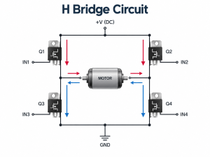
H bridge circuit diagram with four MOSFETs and a DC motor

What Is an H Bridge Circuit and What Is It Used For?

An H bridge circuit controls the direction of current through a load by switching its two terminals between the power supply and ground.

The circuit normally contains:

  • Two high-side switches
  • Two low-side switches
  • A DC supply
  • A load connected between the two switching legs
  • Control signals for the four switches

Its name comes from the traditional circuit diagram. The four switching devices form the sides of an imaginary “H,” while the motor or load sits across the center.

The main purpose of an H bridge is polarity reversal. Instead of physically swapping the wires connected to a DC motor, the switches reverse the voltage across the motor electronically.

Common applications include:

  • DC motor forward and reverse control
  • PWM motor speed control
  • Motor braking
  • Solenoids and actuators
  • Robotics and motion systems
  • Bidirectional current control
  • Class-D output stages
  • DC-to-AC inverter stages

For a brushed DC motor, reversing armature current reverses motor rotation. That is why the H bridge has become a standard circuit in motor-control electronics.

What Does an H Bridge Circuit Diagram Show?

An H bridge circuit diagram shows four switches arranged in two legs, with the motor connected between the two switching nodes.

H bridge circuit diagram showing forward and reverse current paths through a DC motor

A typical MOSFET H bridge includes:

  • Q1: left high-side MOSFET
  • Q2: left low-side MOSFET
  • Q3: right high-side MOSFET
  • Q4: right low-side MOSFET

The circuit changes motor polarity by turning on opposite diagonal MOSFETs.

Active MOSFETs Left Motor Terminal Right Motor Terminal Result
Q1 + Q4 High Low Current in one direction
Q2 + Q3 Low High Current in the opposite direction
All OFF Floating Floating Coast
Both motor terminals at the same potential Same Same Brake

Switch labels differ between schematics, so it is more useful to follow the current path than memorize Q1, Q2, Q3, and Q4 positions.

One switching rule is critical: the high-side and low-side MOSFET in the same leg must not conduct at the same time. Otherwise, they can create a direct path from the supply rail to ground. This condition is called shoot-through.

How Does an H Bridge Circuit Work for a DC Motor?

An H bridge controls a DC motor by reversing the voltage polarity across its two terminals.

H bridge DC motor control states showing forward, reverse, coast, and brake

For forward rotation, one high-side MOSFET and the diagonally opposite low-side MOSFET conduct. Current flows through the motor in one direction.

For reverse rotation, the opposite diagonal pair turns on. The motor current reverses, so the motor rotates the other way.

H Bridge State Switching Condition Motor Response
Forward First diagonal pair ON Forward rotation
Reverse Opposite diagonal pair ON Reverse rotation
Coast All switches OFF Motor slows freely
Brake Motor terminals held at similar potential Faster deceleration

PWM is normally used when speed control is also required. The controller rapidly switches the bridge and changes the duty cycle to adjust the average voltage applied to the motor.

Motor current should be checked carefully before selecting the power stage. Important values include:

  • Normal running current
  • Startup current
  • Stall current
  • Current during rapid direction reversal
  • Expected PWM duty cycle

Stall current is particularly important because it can be several times higher than normal operating current. MOSFETs, PCB copper, connectors, and the power supply must all tolerate this condition.

Half H Bridge vs Full H Bridge Circuit: What Is the Difference?

A half bridge uses one pair of switches, while a full H bridge uses two half-bridge legs and normally contains four switches.

Half bridge versus full H bridge circuit comparison
Feature Half Bridge Full H Bridge
Main switches 2 4
Switching legs 1 2
Output One switched midpoint Two switched midpoints
Load polarity reversal Not by itself Yes
DC motor reversing Requires additional circuitry Directly supported
Typical applications Power conversion, inverter legs Motors, actuators, full-bridge inverters

In a half bridge, the output switches between the upper and lower supply rails.

A full H bridge places the load between two half-bridge switching nodes. Because either side of the load can be driven high or low, the voltage across it can be reversed.

For this reason, a full H bridge is normally used when a DC motor needs both forward and reverse operation.

How Do You Design an H Bridge Circuit Using MOSFETs?

A MOSFET H bridge should be designed from the actual supply voltage, motor current, switching frequency, and thermal conditions.

The most important MOSFET parameters are below.

Drain-source voltage

The MOSFET VDS rating must exceed the highest voltage it may see in operation, including supply tolerance and switching overshoot.

Motor windings are inductive, so the peak drain voltage can be higher than the nominal DC bus voltage.

Current rating

Do not size the MOSFET from running current alone. Check:

  • Continuous motor current
  • Startup current
  • Stall current
  • Short-duration peak current
  • Expected board and ambient temperature

Datasheet current ratings are strongly affected by package temperature and PCB thermal conditions.

RDS(on)

MOSFET conduction loss can be estimated with:

P = I² × RDS(on)

Low RDS(on) becomes increasingly important as motor current rises. Use the resistance expected at the real junction temperature rather than relying only on the 25°C typical value.

Gate charge

Gate charge affects how quickly the MOSFET can switch. A device with very low RDS(on) may have a larger gate charge, which requires more current from the gate driver. Slow transitions increase switching loss.

High-side drive

A high-side N-channel MOSFET usually needs a gate voltage above its source voltage.

Common drive methods include:

  • Bootstrap gate drivers
  • Charge-pump drivers
  • Isolated gate-driver supplies

Low-voltage circuits sometimes use P-channel MOSFETs on the high side because they are easier to drive, although their RDS(on) is often higher.

PWM frequency

PWM frequency affects both control behavior and switching loss. A higher frequency may move switching noise above the audible range, but it also increases switching events per second.

The final choice should suit the motor, MOSFET, driver, and thermal budget rather than being selected in isolation.

How Do You Prevent Shoot-Through and Inductive Voltage Spikes?

Shoot-through is controlled with correct gate timing, while inductive voltage spikes are controlled by giving motor current a safe path when the MOSFETs switch.

MOSFET H bridge protection showing gate driver, dead time, bus capacitor, and recirculation path

Shoot-through prevention

Shoot-through happens when both MOSFETs in the same bridge leg conduct simultaneously.

Possible results include:

  • Very high supply current
  • MOSFET overheating
  • Gate-driver damage
  • Supply voltage collapse
  • PCB or connector damage

The usual solution is dead time. One MOSFET is allowed to turn fully off before the complementary MOSFET turns on.

Required dead time depends on:

  • MOSFET switching characteristics
  • Gate charge
  • Gate resistance
  • Driver source and sink current
  • Propagation delay

Too little dead time risks cross-conduction. Too much increases body-diode conduction and power loss.

Inductive voltage control

Motor current cannot stop instantly when a MOSFET turns off. The stored magnetic energy must continue flowing through another path.

Depending on the design, this path may use:

  • MOSFET body diodes
  • External diodes
  • Synchronous MOSFET conduction
  • TVS devices
  • Snubber circuits
  • Local bus capacitors

The protection components should be selected from the actual motor current and measured switching waveform, not only from the nominal supply voltage.

H Bridge IC vs Discrete MOSFETs: Which Should You Use?

An H bridge IC is usually easier for compact low- or medium-power designs, while external MOSFETs provide more flexibility for higher-current applications.

Design Best Fit
Integrated H bridge IC Compact, lower-power designs
Driver IC + external MOSFETs Medium- to high-power motor control
Discrete bridge Highly customized power stages

An integrated H bridge IC may include:

  • Power switches
  • Gate drivers
  • Overcurrent protection
  • Thermal shutdown
  • Undervoltage lockout
  • Current sensing
  • Fault reporting

This reduces component count and simplifies the PCB.

External MOSFETs are useful when the design requires:

  • Higher motor current
  • Higher bus voltage
  • Lower conduction loss
  • Better heat spreading
  • Specific MOSFET packages
  • Custom switching behavior

Many practical motor controllers use a gate-driver IC with four external N-channel MOSFETs. This keeps the control function integrated while allowing the power devices to be selected separately.

What PCB Layout Rules Matter for an H Bridge Circuit Board?

An H bridge circuit board should keep high-current and high-speed switching paths short while separating noisy switching nodes from sensitive control signals.

H bridge PCB layout with high-current copper, decoupling, gate driver, thermal vias, current sense, and oscilloscope testing

The most important PCB layout rules are:

  • Keep the DC bus switching loop compact.
  • Place local ceramic decoupling close to the MOSFET bridge.
  • Keep gate-driver traces short.
  • Provide a direct gate-return path.
  • Keep switching-node copper away from analog and control signals.
  • Size power copper for peak motor current, not only running current.
  • Provide adequate thermal copper under power MOSFETs.
  • Use thermal or current-sharing vias where required.
  • Route current-sense connections separately from motor current paths.

The bus capacitor is especially important. If it is too far from the MOSFET bridge, the extra trace inductance can increase drain-voltage ringing.

High-current H bridge boards may require more than ordinary trace widening. Depending on current and thermal limits, the PCB can use:

  • Large copper pours
  • Heavier copper
  • Parallel copper layers
  • Dense via arrays
  • Copper inlays or busbars

Switching-node copper should be large enough for electrical and thermal needs but not unnecessarily oversized. Large high-dV/dt areas increase capacitive coupling and EMI.

Current-sense circuits also deserve careful routing. Kelvin connections should be used where a low-value shunt resistor is measured, and its sense traces should be kept away from fast switching nodes.

How Do You Simulate and Test an H Bridge Circuit?

H bridge simulation should verify switching timing and device stress, while prototype testing should confirm the actual waveforms, current, and temperature on the assembled PCB.

Useful simulation results include:

  • High-side and low-side gate waveforms
  • Dead time
  • Motor current
  • Current reversal
  • PWM behavior
  • Switching-node voltage
  • Drain-source voltage
  • Voltage overshoot
  • MOSFET power loss
  • DC bus ripple

Ideal switch models are useful for learning the basic H bridge operation, but realistic MOSFET and diode models are more useful when checking switching loss or transient behavior.

After assembly, test the board under realistic operating conditions.

Typical measurements include:

  • MOSFET gate-source voltage
  • Bridge switching-node waveform
  • Motor startup current
  • Stall or near-stall current
  • Direction-reversal behavior
  • DC bus overshoot
  • MOSFET temperature
  • Connector and copper temperature

Testing should cover the expected supply voltage, motor load, PWM duty cycle, ambient temperature, and operating time.

A motor that runs correctly at no load does not prove that the H bridge can handle startup, stall, braking, or repeated direction changes.

Use appropriate measurement equipment when probing high-side or floating switching nodes. A differential probe or isolated measurement method may be required to avoid creating an accidental short through the oscilloscope ground.

FAQ

1. Why is it called an H bridge circuit?

Because the traditional circuit diagram resembles the letter H. Four switches form the sides, and the motor or load connects across the middle.

2. Can an H bridge control motor speed and direction?

Yes. The H bridge reverses motor direction by changing polarity, while PWM controls the average voltage used for speed control.

3. What is the difference between a half bridge and a full H bridge?

A half bridge has one switching leg with two switches. A full H bridge has two switching legs and normally four switches, allowing the load voltage to reverse.

4. What causes shoot-through in an H bridge circuit?

Shoot-through occurs when the high-side and low-side MOSFET in the same leg conduct at the same time. Proper dead time prevents this condition.

5. Can an H bridge circuit be used as an inverter?

Yes. A full H bridge can alternate the polarity across a load and is commonly used in inverter power stages.

6. What is a dual H bridge circuit?

A dual H bridge contains two independent H bridge channels. It can drive two bidirectional DC motors or other loads from one circuit or IC.

Need Support With an H Bridge PCB or PCBA Project?

An H bridge PCB has to carry motor current while controlling fast switching edges, heat, gate timing, and inductive transients within the same board.

EBest Circuit supports PCB fabrication and PCBA for motor-control and power-electronics projects. If you are preparing an H bridge circuit board, send your Gerber files, BOM, schematic or fabrication drawing, operating voltage, motor current, and quantity to sales@bestpcbs.com for engineering review and quotation.

You may also like

How to Add a New Copper Layer to KiCad 9: Step-by-Step Guide

September 10th, 2026

To add a new copper layer to KiCad 9, open PCB Editor → File → Board Setup → Board Stackup → Physical Stackup, then increase the copper layer count. For example, changing a two-layer PCB to four layers adds the internal copper layers In1.Cu and In2.Cu.

Adding a copper layer is different from adding a copper zone. A copper layer changes the physical PCB stackup. A copper zone places copper on an existing layer for ground, power, shielding, or current distribution. Knowing which one you need avoids unnecessary setup changes.

How to add a new copper layer to KiCad 9 in a four-layer PCB design

How to Add a New Copper Layer to KiCad 9?

To add copper layers in KiCad 9, change the layer count in Physical Stackup.

  1. Open the PCB layout in PCB Editor.
  2. Go to File → Board Setup.
  3. Select Board Stackup → Physical Stackup.
  4. Find the Copper layers setting.
  5. Change the board from 2 layers to 4 layers, or select another supported layer count.
  6. Review the new internal copper layers.
  7. Click OK.
KiCad 9 Physical Stackup changing a PCB from two copper layers to four copper layers

A standard four-layer board will normally include:

  • F.Cu
  • In1.Cu
  • In2.Cu
  • B.Cu

KiCad 9 uses an even number of physical copper layers, so a two-layer design normally moves to four layers rather than three.

After increasing the layer count, check the stackup values instead of treating them as placeholders. Useful items to review include:

  • Copper thickness
  • Dielectric thickness
  • Overall board thickness
  • Layer order
  • Material type

Do not use Add User Defined Layer to create another electrical copper layer. User-defined layers are intended for drawings, notes, fabrication information, or other non-routing content.

Copper Layer vs Copper Zone in KiCad 9: What Is the Difference?

A copper layer is a physical conductive layer in the PCB, while a copper zone is an area of copper created on an existing layer.

Item Copper Layer Copper Zone
Main purpose Adds a physical PCB layer Adds copper within an existing layer
Examples F.Cu, In1.Cu, In2.Cu, B.Cu GND pour, power plane
Setup location Physical Stackup Add Filled Zone
Changes PCB layer count Yes No
Assigned to a net Not by itself Usually yes
Comparison between physical copper layers and a copper zone in KiCad 9

For example, adding In1.Cu gives the PCB another physical copper layer. It does not automatically turn that layer into a ground plane.

If you want In1.Cu to work as ground, create a copper zone on that layer and assign it to the GND net.

This distinction matters because many searches for “how to add copper layer in KiCad” actually come from users who only need a ground or power pour.

How to Add a Ground Plane in KiCad 9?

To add a ground plane in KiCad 9, create a filled copper zone and assign it to the GND net.

  1. Select the copper layer where the plane should be created.
  2. Click Add Filled Zone.
  3. Click inside the PCB outline.
  4. Select the GND net.
  5. Confirm the target copper layer.
  6. Draw the zone boundary around the required area.
  7. Finish the outline.
  8. Press B to refill all zones.
How to add a GND filled copper zone and ground plane in KiCad 9

On a two-layer PCB, a GND zone is often placed on B.Cu. On a four-layer board, an internal layer such as In1.Cu may be used as a more continuous ground reference.

The zone boundary only defines where KiCad is allowed to calculate copper. The actual filled shape depends on traces, vias, pads, clearances, cutouts, and design rules. After routing changes, press B again so the copper fill reflects the latest layout.

Which KiCad Copper Zone Properties Should You Set?

The most important KiCad copper zone properties are the net, layer, clearance, minimum width, pad connection, and thermal relief settings.

  • Layer: Sets where the zone is placed.
  • Net: Connects the zone to GND, power, or another net.
  • Clearance: Controls spacing from copper on other nets.
  • Minimum width: Removes copper areas that become too narrow.
  • Pad connections: Sets solid, thermal relief, or no connection.
  • Thermal relief gap: Defines spacing around thermally connected pads.
  • Thermal spoke width: Sets the width of each thermal connection.
  • Fill style: Selects solid or hatched copper.
  • Island removal: Controls how disconnected copper islands are handled.

The values should match both the electrical requirement and the PCB manufacturer’s design rules. Clearance and minimum width deserve particular attention because they can directly change the final filled geometry.

Thermal relief settings also affect assembly. A large solid copper plane can pull heat away from a pad during soldering, while thermal spokes reduce that heat transfer.

How Does KiCad Zone Priority Work?

KiCad zone priority controls which overlapping copper zone is filled first.

A higher-priority zone is calculated before a lower-priority zone. The lower-priority zone then keeps the required clearance from the copper already created.

A common example is:

  • A large GND zone across most of the layer
  • A smaller +5V zone inside part of the same area

If the +5V area must remain inside the larger ground region, the power zone can be given a higher priority.

KiCad copper zone properties and zone priority for overlapping GND and 5V zones

Zone priority is useful when two or more copper zones intentionally overlap. It is not a fix for an incorrect net, poor outline, or unsuitable clearance setting.

If overlapping zones behave unexpectedly, check:

  • Net assignment
  • Target layer
  • Zone outline
  • Clearance
  • Priority value

For layouts with several zones, the Zone Manager makes it easier to compare their settings in one place.

Why Is the KiCad Ground Plane Not Filling?

If a KiCad ground plane is not filling, press B first to refill all zones.

If the problem remains, check:

  • Wrong net: Confirm that the zone is assigned to GND.
  • Wrong layer: Make sure the zone is on the copper layer you are viewing.
  • Incomplete outline: Check that the zone boundary is closed.
  • Large clearance: Too much spacing can remove copper from narrow areas.
  • Large minimum width: Narrow copper sections may be discarded.
  • Keepout or rule area: These may block copper from filling.
  • Board cutout: Copper will not fill through cutouts or outside the board edge.
  • Island removal: Small disconnected copper areas may be removed automatically.
  • Hidden fill display: The zone may be filled but only its boundary is visible.

If only one section of the plane is missing, inspect that local area closely. Dense vias, BGA fanout, narrow board sections, or nearby keepouts often create the problem. After making changes, refill the zones and run DRC again.

How to Hide Filled Zones in KiCad Without Deleting Them?

To hide filled zones in KiCad, switch the PCB Editor to show only the zone boundaries.

This changes the display only. It does not remove the copper zone from the design.

  • Hide zone fill: Keeps the zone but hides the rendered copper.
  • Unfill zone: Removes the calculated fill until it is filled again.
  • Delete zone: Removes the zone object completely.

Hiding the fill is useful when large power or ground areas make routing difficult to see. If a copper zone suddenly appears to be missing but its outline is still visible, check the display mode before changing the design.

What Should You Check Before Fabricating a Multilayer KiCad PCB?

Before fabricating a multilayer KiCad PCB, confirm that the KiCad stackup matches a stackup your PCB manufacturer can actually build.

KiCad 9 multilayer PCB fabrication review with Gerber stackup via and impedance checks

Check these items before releasing fabrication data:

  • Copper layer count: Make sure all intended layers are included.
  • Layer order: Confirm the correct position of signal, ground, and power layers.
  • Board thickness: Verify the finished PCB thickness.
  • Copper thickness: Confirm outer- and inner-layer copper requirements.
  • Dielectric structure: Review core and prepreg thicknesses.
  • Controlled impedance: Confirm material, dielectric thickness, copper thickness, and target impedance.
  • Via structure: Check through holes, blind vias, buried vias, or microvias.
  • Plane continuity: Look for fragmented ground or power planes.
  • Zone fill: Press B before final output.
  • DRC: Resolve relevant clearance and connectivity errors.
  • Gerber and drill data: Confirm that every copper and drill layer is exported correctly.

A four-layer board created in KiCad is not automatically a production-ready four-layer stackup. The PCB factory may use different prepreg thicknesses, core materials, or copper weights from the default CAD values.

For controlled-impedance boards, confirm the production stackup before finalizing critical trace widths. A dielectric change can alter the impedance even when the routing geometry stays the same.

If your KiCad design is ready for fabrication, EBest Circuit can review the Gerber files, stackup, material selection, copper weight, via structure, and impedance requirements before production.

For schematic net naming, see our guide to how to make labels in KiCad.

FAQ About Adding Copper Layers in KiCad 9

1. Can I add only one new copper layer in KiCad 9?
No. KiCad 9 uses an even number of physical copper layers, so a two-layer PCB normally changes to four layers rather than three.

2. How do I change a KiCad PCB from 2 layers to 4 layers?
Open PCB Editor → File → Board Setup → Board Stackup → Physical Stackup, then change the copper layer count from 2 to 4.

3. Is In1.Cu automatically a ground plane in KiCad?
No. In1.Cu is only an internal copper layer. Create a copper zone on it and assign that zone to GND if you want to use it as a ground plane.

4. What is the shortcut to refill copper zones in KiCad?
Press B to refill all copper zones.

5. Why did my copper fill disappear in KiCad?
The fill may be hidden, unfilled, blocked by clearance rules, or removed by zone settings. Check the display mode first, then refill the zone with B.

6. Can one copper zone be used on multiple layers in KiCad 9?
Yes. A zone can be assigned to multiple copper layers while using the same net, with the copper fill calculated separately on each selected layer.

Adding a new copper layer in KiCad 9 is simple once you use the correct stackup settings. The more important step is making sure the final layer structure, zones, vias, and fabrication data match the PCB you actually want to manufacture.

For PCB fabrication or PCBA support, send your Gerber files, stackup requirements, material requirements, copper weight, impedance targets, and quantity to sales@bestpcbs.com for DFM review.
You may also like

Thick PCB Board vs Heavy Copper PCB: Design and Selection Guide

September 10th, 2026

A thick pcb board and a heavy copper PCB solve different engineering problems. The first increases the total finished thickness of the board; the second increases the copper thickness on selected or all conductive layers. A board can be mechanically thick without carrying high current, and a heavy copper design can fit inside a conventional overall thickness.

This distinction affects stackup planning, hole sizes, impedance, thermal behavior, connector fit, manufacturing cost, and the information a fabricator needs before quotation. This guide compares the two constructions so engineers and buyers can specify the right one instead of treating “thick board” and “thick copper” as interchangeable terms.

Thick PCB board versus heavy copper PCB engineering comparison

What Is a Thick PCB Board?

A thick PCB board is a rigid printed circuit board whose total finished thickness is greater than the common construction used for a similar product. The measurement spans the complete board from one outer surface to the other. It includes cores, cured prepregs, copper layers, plating, solder mask, and smaller finish contributions.

The term describes a mechanical dimension, not a specific copper weight. Designers may choose a thicker construction to:

  • Increase stiffness across a large unsupported area.
  • Support transformers, relays, power modules, large connectors, or other heavy components.
  • Meet card-edge, press-fit, guide-rail, enclosure, or mounting requirements.
  • Fit additional routing and reference-plane layers into a multilayer stackup.
  • Provide required dielectric spacing between conductors.
  • Control bending in equipment exposed to vibration or mechanical handling.

A thick board should not be selected only because it appears stronger. Extra thickness can create higher hole aspect ratios, longer routing cycles, different depaneling limits, more material usage, and tighter connector-fit constraints.

How Thick Is a PCB Board?

The practical answer to “how thick is a pcb board” depends on the application and the complete stackup. Many rigid FR-4 boards use a finished thickness near 1.6 mm, while thinner products may use 0.8, 1.0, or 1.2 mm. Mechanically demanding or high-layer-count designs may use 2.0, 2.4, 3.2 mm, or another project-specific value.

These numbers are not automatic manufacturing categories. A 2.4 mm two-layer board with generous holes is usually less demanding than a 2.4 mm multilayer board with small plated holes, controlled impedance, heavy outer copper, and a strict finished-thickness tolerance. The fabricator must review the thickness together with:

  • Layer count and copper distribution.
  • Core and prepreg constructions.
  • Smallest drilled and finished hole sizes.
  • Plated-through, blind, buried, or filled via structures.
  • Controlled-impedance geometries.
  • Board dimensions, panelization, and routing method.
  • Connector, press-fit, and enclosure tolerances.

For a broader dimensional reference, see our guide to standard printed circuit board thickness.

What Is the Standard PCB Thickness?

The question “what is the standard pcb thickness” usually refers to 1.6 mm, approximately 0.062 inch. It is a widely used rigid-board value because common laminate constructions, connectors, housings, fixtures, and assembly processes are often designed around it. However, 1.6 mm is a common default rather than a universal rule.

Finished thickness is built from real laminate and prepreg options. Prepreg does not behave like a fixed spacer: its pressed thickness changes with glass style, resin content, copper pattern density, resin flow, and the lamination cycle. Material suppliers such as Isola publish laminate and prepreg construction data that fabricators use when developing manufacturable stackups.

If a mechanical drawing calls out only an unusual finished thickness but does not define the stackup, the designer should let the PCB manufacturer propose available core and prepreg combinations. This is safer than forcing a theoretical build that depends on unavailable materials or unrealistic pressed thicknesses.

PCB board thickness compared with copper thickness in cross-section

Thick PCB Board vs Heavy Copper PCB: What Is the Difference?

The shortest distinction is simple: board thickness is a mechanical stack dimension, while copper thickness is a conductor dimension. They influence different parts of PCB performance and manufacturing.

Comparison Thick PCB Board Heavy Copper PCB
Primary definition Greater total finished board thickness Greater copper thickness or copper weight on one or more layers
Main purpose Mechanical stiffness, stackup space, connector fit, or dielectric spacing High-current conduction, lower conductor resistance, heat spreading, or robust power connections
Most affected design data Stackup, hole size, aspect ratio, impedance, enclosure, routing, and tolerance Trace width and spacing, pad geometry, etching, resin fill, plating, current rise, and thermal path
Typical manufacturing concern Deep drilling, hole preparation, plating coverage, lamination, routing, and warpage control Etch compensation, copper balance, resin filling around tall conductors, conductor definition, and thermal mass
Can it exist without the other? Yes. A thick board can use standard copper. Yes. A heavy copper board can retain a conventional finished thickness.

For example, a 3.2 mm FR-4 board with 1 oz copper is mechanically thick but is not a heavy copper PCB. A 1.6 mm board with 4 oz copper is a heavy copper design even though its total thickness is conventional. Some power products need both: a thick structure for stiffness and thick copper for electrical and thermal performance.

How Does a Thick Board Change Stackup and Impedance?

Increasing total board thickness changes the dielectric distance available between copper layers. If trace width, copper thickness, and dielectric properties remain unchanged, a larger trace-to-reference-plane distance changes characteristic impedance. Therefore, a designer cannot simply stretch every dielectric layer to reach a new finished thickness and expect the same controlled-impedance result.

A practical thick-board stackup review covers:

  • Reference-plane location: High-speed signals still need a nearby and continuous return plane.
  • Dielectric selection: Core and prepreg choices must match available material constructions and the required pressed thickness.
  • Copper balance: Symmetric copper and dielectric distribution helps reduce lamination stress and bow or twist.
  • Resin filling: Heavy copper or uneven pattern density may require higher-resin prepreg to fill around conductors.
  • Finished tolerance: The stackup must leave a realistic process window for material and lamination variation.

Do not approve the mechanical thickness independently from impedance. Send the impedance table, target values, referenced layers, and any material restrictions with the stackup so the fabricator can model the construction as one system.

How Do Drilling and Plating Limits Change?

As a board becomes thicker, a mechanically drilled hole becomes deeper. If the drill diameter stays small, the hole aspect ratio rises. This makes debris removal, desmear, activation, and copper deposition inside the barrel more demanding. The result can be thin plating in the center of the hole, barrel voids, poor registration margin, or lower thermal-cycling reliability.

Aspect ratio is commonly expressed as board thickness divided by drilled hole diameter. It is a DFM relationship, not a target that should be pushed without considering the material, layer count, plating process, copper requirement, and acceptance class. A thicker finished board may need one or more of the following changes:

  • Increase the mechanically drilled hole diameter.
  • Use staged or controlled drilling conditions.
  • Adjust the via structure instead of using one deep through-hole.
  • Increase annular-ring and registration allowance where required.
  • Specify hole-wall copper and microsection acceptance clearly.
  • Review press-fit hole tolerances and final plating buildup.
Thick PCB plated through-hole and drilling aspect ratio

IPC-6012F establishes qualification and performance requirements for rigid printed boards, including multilayer constructions with plated-through, blind, buried, and microvia structures. The applicable class, customer drawing, procurement specification, and agreed deviations should be defined before production.

Heavy Copper PCB Design: What Must Be Reviewed?

Heavy copper PCB design starts with electrical and thermal requirements, not with a higher copper weight chosen by habit. A thicker conductor can reduce resistance and support more current, but the result also depends on trace width, conductor location, ambient conditions, allowed temperature rise, adjacent copper, airflow, duty cycle, terminal design, and heat-transfer paths.

IPC-2152 provides guidance on the relationship between current, conductor dimensions, and acceptable temperature rise. It is a better basis for conductor sizing than assuming that a mechanically thicker board will automatically carry more current.

Manufacturing review should include:

  • Copper weight required on every inner and outer layer.
  • Minimum line width and spacing after etch compensation.
  • Pad, via, and neck-down geometry at high-current transitions.
  • Resin filling around tall copper features.
  • Copper balance across the panel and stackup.
  • Thermal reliefs, solderability, and assembly heat demand.
  • Finished copper and plated-hole copper acceptance.
Heavy copper PCB design for high current and heat spreading

EBest Circuit supports heavy copper PCB projects for power distribution, heat spreading, planar transformers, power converters, and related high-current applications. Exact copper, spacing, stackup, and test requirements must be confirmed against the production data.

Which Construction Should You Choose?

Choose the construction from the problem you are trying to solve. Mechanical stiffness does not replace electrical conductor sizing, and additional copper does not guarantee connector fit or board rigidity.

Primary Requirement Review First Likely Direction
Large board or heavy components need more rigidity Board dimensions, mounting points, vibration, and enclosure support Thicker finished board
High current with an acceptable temperature rise Current, trace width, copper weight, duty cycle, and cooling Heavy copper PCB
More routing and reference planes Layer count, impedance, dielectric spacing, and via structure Thicker multilayer stackup, if required
High current plus mechanical stiffness All electrical, thermal, stackup, drilling, and enclosure constraints Combined thick-board and heavy-copper construction
Connector or card-edge fit Specified finished thickness and tolerance at the mating interface Board thickness driven by connector geometry

If the design needs both thickness and heavy copper, review them together before layout release. Thick copper consumes vertical space, changes resin demand, restricts fine features, and can alter the final thickness. A late copper-weight change can therefore invalidate the stackup and controlled-impedance calculations.

What Should You Send for a Manufacturing Review?

A useful DFM package lets the fabricator evaluate the mechanical and conductor requirements separately, then confirm how they interact. Include:

  • Gerber or ODB++ fabrication data and drill files.
  • Layer count and proposed stackup.
  • Target finished board thickness and tolerance.
  • Base material, Tg, CTI, thermal, or high-frequency requirements.
  • Copper weight for every layer and any selective heavy-copper areas.
  • Smallest drilled hole, smallest finished hole, via types, and filled-via requirements.
  • Controlled-impedance values and referenced layer pairs.
  • Board dimensions, panel or delivery format, outline tolerance, and connector requirements.
  • Surface finish, solder mask, legend, electrical test, acceptance class, and required reports.
  • Prototype and production quantities plus the required delivery date.

If the project is already defined as a thick mechanical build, our thick PCB board manufacturing guide explains the detailed stackup and quotation review path.

FAQ About Thick PCB Boards and Heavy Copper PCBs

Is a 2.0 mm PCB considered thick?

It is thicker than the common 1.6 mm construction, but whether it needs special processing depends on its layer count, material, dimensions, holes, copper weight, tolerances, and routing method.

Does a thick PCB carry more current?

Not automatically. Current capacity is primarily determined by conductor geometry, temperature-rise limits, copper environment, cooling, and operating conditions. Overall board thickness is a separate mechanical property.

Can a heavy copper PCB be only 1.6 mm thick?

Yes. A fabricator may build heavy copper into a conventional finished thickness if the layer structure, dielectric spacing, resin fill, feature sizes, and tolerance can be manufactured reliably.

Why are small vias difficult in a thick board?

The deeper hole creates a higher aspect ratio. Hole cleaning and uniform copper deposition become more demanding, especially when the finished hole is small or the specified barrel copper is high.

Should I specify copper in ounces or micrometers?

Either can be used if the procurement documents are consistent, but clearly distinguish base copper from finished copper after plating. State the requirement for each layer rather than using one value for the entire PCB.

Can board thickness be changed after impedance routing is complete?

Only after the impedance geometry is recalculated. Changing the dielectric distance to the reference plane can change impedance, so the fabricator must review the revised stackup, trace width, spacing, copper thickness, and material properties.

How Can EBest Circuit Support Your PCB Project?

EBest Circuit reviews thick-board and heavy-copper requirements as two connected but distinct engineering inputs.

Send your Gerber or ODB++ data, stackup, finished thickness, copper weight by layer, drill table, impedance requirements, material notes, surface finish, test standard, quantity, and delivery target to sales@bestpcbs.com. We will review the manufacturable construction before quotation and prototype release.

You may also like

Cleaning Electronics With Rubbing Alcohol: 70%, 90%, or 99% IPA?

September 10th, 2026

Cleaning electronics with rubbing alcohol can be safe when the device is disconnected from power, the liquid is kept out of openings, and the concentration matches the surface. For exposed PCBs, 90% to 99% electronics-grade isopropyl alcohol (IPA) is usually a better starting point than 70% rubbing alcohol because it contains less water and dries faster.

That does not make IPA a universal electronics cleaner. Display coatings, printed legends, adhesives, unsealed sensors, and some plastics may be damaged. The contamination also matters: IPA can lift oils and many rosin-based flux residues, but it may not remove salts, sugary spills, water-soluble flux, or cured residues.

Technician cleaning a powered-off PCB at an ESD-safe workbench with rubbing alcohol

Can You Clean Electronics With Rubbing Alcohol?

Yes, you can clean selected electronics with rubbing alcohol after removing power and confirming that the device maker permits alcohol on the target surface. A slightly damp lint-free cloth may be suitable for an approved hard exterior, while an exposed PCB normally calls for controlled application of 90% to 99% electronics-grade IPA.

First decide which job you are doing:

  • Exterior wiping: Some manufacturers permit 70% IPA wipes on hard, nonporous surfaces. Apple and Dell publish product-specific examples, but their instructions do not apply automatically to every device.
  • Exposed-board cleaning: Repair guides commonly use at least 90% IPA for localized work on a disconnected logic board or PCB.
  • Disinfection: The concentration and wet contact time needed to disinfect a surface are different from the requirements for removing flux or oil from a circuit board.

Never spray alcohol directly onto a device. Wet the cloth, foam swab, polyester swab, or ESD-safe brush away from the electronics, then apply only enough liquid to loosen the soil.

Is Rubbing Alcohol Safe for Electronics?

Rubbing alcohol is safe only for compatible materials and controlled, unpowered cleaning; it is not safe to pour into an assembled device or use around ignition sources. A 70% IPA wipe may be approved for a laptop shell or keyboard, yet the same liquid can enter a connector, remain beneath a shield, soften adhesive, or mark a coated display.

This is why the answer to whether rubbing alcohol is safe for electronics depends on the exact part, contamination, and application method rather than the device category alone.

The label matters as much as the percentage. A bottle sold as first-aid rubbing alcohol is formulated for topical use, not residue-sensitive PCB production. Many 70% products contain 30% water, and formulations vary by supplier. Before use, check the active ingredients, inactive ingredients, and safety data rather than assuming every clear alcohol product is equivalent.

IPA is also highly flammable. NIOSH lists isopropyl alcohol as a Class IB flammable liquid with a 53°F (12°C) flash point. Keep it away from soldering irons, hot-air rework tools, sparks, smoking, and open flame; cap the container when not in use and provide ventilation.

What Percentage Isopropyl Alcohol for Electronics?

Use the device maker’s approved product for finished equipment; for localized exposed-PCB cleaning, 90% to 99% electronics-grade IPA is the practical starting range because it contains only 1% to 10% water instead of the 30% found in 70% IPA. Higher purity does not override component, coating, or adhesive restrictions.

IPA Concentration Approximate Water Content Suitable Starting Use Main Limitation
70% 30% Approved hard exterior surfaces using a damp wipe Slower drying and more water; not the default for exposed PCBs
90% or 91% 9% to 10% Localized PCB repair and residue removal when compatible Can still affect coatings, plastics, markings, and adhesives
99% or 99.9% 0.1% to 1% Moisture-sensitive, residue-controlled bench cleaning Still flammable and not effective against every contaminant
Comparison of 70 percent, 90 percent, and 99 percent IPA for exterior and exposed PCB cleaning

Do not dilute high-purity IPA with tap water for PCB work. Tap water can add minerals and ions. If an aqueous process is required, it should use chemistry, rinse-water quality, and drying conditions chosen for the assembly.

What Is the Difference Between Rubbing Alcohol and Electronics-Grade IPA?

Household rubbing alcohol is usually sold as a skin antiseptic, whereas electronics-grade IPA is supplied with controlled purity and residue expectations for cleaning components and assemblies. A common 70% first-aid product is 70 mL IPA per 100 mL with water as the inactive ingredient; an electronics cleaner may be 99.9% anhydrous IPA with a technical data sheet and safety data sheet.

Do not judge a cleaner by the front label alone. Check:

  • IPA concentration and water content;
  • listed fragrance, dye, oil, bitterant, or other additive;
  • nonvolatile residue specification, if provided;
  • plastics, elastomer, coating, and adhesive compatibility;
  • storage, ventilation, and personal-protection instructions in the SDS.

For a repeatable manufacturing process, lot-controlled cleaner and documented compatibility are more useful than a generic pharmacy bottle whose intended use is first aid.

Which Parts Should Not Be Cleaned With Rubbing Alcohol?

Do not apply rubbing alcohol to an unapproved display coating, printed key legend, foam adhesive, acrylic or polycarbonate part, unsealed microphone, speaker, sensor, relay, or coated PCB area without a material check. Even when the bare laminate and solder mask tolerate IPA, a complete assembly may contain liquid-trapping or solvent-sensitive parts.

Display coating, printed legends, adhesive tape, and an unsealed sensor that require IPA compatibility checks
  • Displays and lenses: Alcohol can affect oleophobic, anti-glare, or other surface treatments unless the manufacturer permits it.
  • Printed markings: Repeated wiping can fade legends on keys, component bodies, labels, and enclosures.
  • Adhesives and foam: IPA is often used to weaken adhesive during repair, which is exactly why it must be controlled near display seals, battery tape, gaskets, and foam pads.
  • Liquid-sensitive devices: Microphones, speakers, MEMS parts, unsealed switches, relays, transformers, and trimmers can trap solvent or suffer mechanical damage.
  • Conformal coating: Cleaning a coated board and intentionally removing coating are different processes. Review the coating chemistry before applying solvent.

How Should You Prepare Electronics Before Cleaning?

Shut the device down, unplug every cable, remove the battery when serviceable, verify stored energy is discharged, and move the work away from sparks, hot tools, and open flame. A power button does not isolate every energy source, and power supplies or large capacitors may retain hazardous voltage after unplugging.

  1. Read the product cleaning or service instructions.
  2. Photograph connectors, cable routing, corrosion, and residue before disassembly.
  3. Disconnect mains power, external supplies, and batteries.
  4. Use an ESD-safe mat, grounded tools, and an ESD-safe brush for sensitive boards.
  5. Remove loose dust first so wet cleaning does not turn it into a paste.
  6. Test the cleaner on a hidden or representative material when compatibility is uncertain.
  7. Use ventilation and keep the IPA container away from ignition sources.

If you cannot safely discharge the equipment, access the board without damaging seals, or identify a swollen battery, stop and use a qualified repair service.

How Do You Clean an Exposed PCB With Isopropyl Alcohol?

Apply a small amount of 90% to 99% electronics-grade IPA to a low-lint swab or ESD-safe brush, loosen the soil, then lift the dissolved residue with clean material instead of letting dirty solvent dry on the board. The goal is removal, not simply spreading a dissolved film across a larger area.

Controlled cleaning of flux residue from an exposed PCB with a low-lint swab
  1. Inspect and classify the soil. Note whether it is dry dust, oil, flux, drink residue, corrosion, or an unknown deposit.
  2. Remove dry particles. Use an ESD-safe soft brush or controlled clean air without forcing debris under packages.
  3. Dampen the tool. Add IPA to the swab or brush away from the PCB; do not pour from the bottle onto the board.
  4. Agitate gently. Work around solder joints and leads without bending parts or snagging fine wires.
  5. Lift the dissolved residue. Blot with a clean low-lint wipe or use fresh solvent as a controlled final rinse.
  6. Replace dirty materials. A brown swab or cloudy solvent is carrying contamination and should not be reused for the final pass.
  7. Dry, inspect, and test. Confirm that connectors, shields, sockets, and package gaps are dry before reconnecting power.

For a broader method covering dust, corrosion, coating, and aqueous cleaning, see our guide to cleaning a PCB board safely.

Which Contaminants Need More Than IPA?

Salt, sugary drinks, water-soluble flux, corrosion products, and unknown deposits may require a qualified aqueous rinse, flux-specific cleaner, or repair process rather than an IPA-only wipe. IPA can evaporate while nonvolatile ionic contamination stays behind.

Contaminant Suitable Starting Method Why IPA Alone May Fail
Finger oil or light grease Compatible high-purity IPA and clean low-lint material Dirty solvent can redeposit an oily film
Rosin-based flux High-purity IPA or matched flux remover after compatibility check Heat-aged or polymerized residue may resist IPA
Water-soluble flux Validated aqueous chemistry and DI-water rinse IPA may not remove the ionic activator system
Sugary or salty spill Controlled aqueous cleaning, DI rinse, and complete drying when parts allow Alcohol can leave conductive nonvolatile material behind
Corrosion Cleaning plus magnified damage assessment and repair Solvent cannot restore missing copper or damaged terminations

Flux chemistry should be identified before selecting the cleaner. Our explanation of flux residue and cleaning methods shows why water-soluble, rosin, and no-clean materials cannot share one blanket instruction.

In our PCBA projects, we treat cleaner selection, rinse quality, drying, and inspection as one process. Changing only the solvent can leave the same ionic residue or hidden moisture problem in a different form.

How Long Should Electronics Dry Before Power-On?

Do not use one universal minute count; restore power only after visible liquid and alcohol odor are gone and no fluid remains trapped under shields, connectors, sockets, switches, or packages. A lightly wiped open surface may appear dry within minutes, while a flooded connector or shielded area can retain solvent much longer.

Use these release checks:

  • no droplets, wet sheen, or cleaner line visible under magnification;
  • no liquid emerging when the board is tilted or gently repositioned;
  • connectors and sockets inspected from more than one angle;
  • no alcohol odor at close range in a ventilated area;
  • no residue film, displaced component, lifted pad, or damaged marking;
  • the device maker’s minimum drying instruction has been met.

Do not use a hot heat gun to accelerate drying. Excessive heat can deform connectors, soften adhesives, damage batteries, or stress solder joints. Use clean dry air or a controlled low-temperature process only when the component limits are known.

What Mistakes Damage Electronics During Alcohol Cleaning?

The highest-risk mistakes are cleaning an energized device, spraying directly into openings, flooding liquid-sensitive parts, using a contaminated swab, and restoring power before trapped solvent has evaporated. Most failures come from uncontrolled application or wrong-material use, not from the word “alcohol” alone.

  • Using 70% as the universal choice: It may be suitable for an approved exterior but adds more water to an exposed assembly.
  • Using a soaked cotton swab: Excess liquid can wick under components, and loose fibers can snag on leads.
  • Letting dirty IPA evaporate: Dissolved flux and oil remain unless they are lifted or rinsed away.
  • Scrubbing harder: Force can remove markings, dislodge 0201/01005 components, bend contacts, or break corroded leads.
  • Ignoring the original fault: Cleaning cannot repair a cracked joint, missing copper, swollen battery, or internally corroded component.
  • Applying conformal coating over residue: Cleanliness and dryness must be verified before coating, or contamination may be sealed onto the assembly.

Production control begins earlier than final cleaning. For example, solder paste inspection in PCB assembly can catch printing defects before placement and reflow, while post-solder cleaning addresses only the residue left by the selected materials and process.

FAQ About Cleaning Electronics With Rubbing Alcohol

These answers cover the most common concentration, surface, flux, and power-on questions about using rubbing alcohol on electronics.

Can I use 70% rubbing alcohol on a circuit board?

Use 70% rubbing alcohol on an exposed circuit board only when the assembly documentation permits it and no better high-purity option is available. Its 30% water content slows drying and raises the chance of liquid remaining in gaps. For localized exposed-PCB cleaning, 90% to 99% electronics-grade IPA is usually the safer starting range.

Is 91% rubbing alcohol good for electronics?

91% IPA is suitable for many localized PCB-repair tasks because it contains about 9% water and evaporates faster than 70%. It can still soften adhesive, affect markings, or enter unsealed parts, so apply a small amount to a low-lint tool and check material compatibility first.

Can I use 99% isopropyl alcohol on a phone screen?

Do not use 99% IPA on a phone screen unless the phone manufacturer explicitly approves it for that model and surface. Screen coatings and display seals vary. Many device makers specify a slightly damp lint-free cloth or a 70% IPA wipe for selected exterior surfaces, not unrestricted use of 99% liquid.

Does isopropyl alcohol remove solder flux?

IPA removes many fresh rosin-based flux residues, especially at 91% to 99%, but it does not remove every no-clean or heat-aged residue. Water-soluble flux normally requires a validated aqueous process. Match the cleaner to the exact flux product and remove the dissolved soil rather than letting it dry on the PCB.

Can cleaning electronics with alcohol cause a short circuit?

Cleaning electronics with alcohol can cause a short circuit if power is present, the liquid contains conductive contamination, or water and dissolved residue remain trapped when the device is energized. Disconnect every power source, control the liquid, dry hidden areas, inspect the board, and only then perform a safe functional test.

Can I pour rubbing alcohol over a motherboard?

Do not pour household rubbing alcohol over an assembled motherboard. Flooding carries dirt beneath packages and into connectors, fans, sockets, microphones, switches, or other liquid-sensitive parts. Board immersion is a specialized repair process that requires disassembly, compatible components, suitable high-purity solvent, ventilation, and controlled drying.

How Can EBest Circuit Support Cleaner, More Reliable PCB Assemblies?

We match the cleaning method to the flux, component set, coating plan, inspection requirement, and end-use risk instead of treating IPA as a universal production solution. At EBest Circuit, we support PCB fabrication, component sourcing, PCB assembly, and inspection within one coordinated project.

For a cleaning-sensitive assembly, send us the Gerber files, BOM, placement data, assembly drawing, target flux or solder-paste specification, coating requirement, quantity, and cleanliness or test criteria. We can review the build information before production and align the inspection plan with the assembly design.

To discuss a PCB or PCBA project, visit our PCB and PCBA manufacturing service page or email sales@bestpcbs.com.

You may also like

FPC Manufacturer UK: Which Supplier Fits Your Project?

September 10th, 2026

FPC manufacturer UK searches lead to companies with very different strengths. Some operate PCB factories in the UK, some specialise in flexible circuits for demanding applications, and others combine local customer support with offshore production. The most useful comparison is therefore not a long directory. It is a clear view of what each manufacturer actually produces and which type of project it suits.

This guide compares five UK manufacturers, shows published FPC process capabilities, and explains where an offshore option may fit. EBest Circuit (Best Technology) manufactures flexible and rigid-flex PCBs for UK customers that need engineering communication, scalable production, and optional assembly through one technical contact. To discuss a released design, email sales@bestpcbs.com with your Gerber or ODB++ data, stack-up, quantity, and application details.

FPC manufacturer UK
Flexible and rigid-flex PCB examples for UK manufacturing projects.

Which FPC Manufacturers Serve UK Projects?

The five companies below have identifiable UK manufacturing operations and publicly describe flexible or rigid-flex PCB capability. They are not ranked because their strongest applications are different.

Manufacturer UK operation Best suited to
GSPK Circuits North Yorkshire General flex, rigid-flex, and specialist PCB projects
Exception PCB Tewkesbury Complex multilayer, HDI, and advanced rigid-flex builds
Merlin Flex Hartlepool Dedicated flex manufacturing and added-value assembly
Amphenol Trackwise Stonehouse Long-length FPCs for aerospace, EV, medical, and industrial systems
Cambridge Circuit Company Cambridge In-house prototypes and fast-turn flex or flex-rigid boards

GSPK Circuits is a broad UK PCB manufacturer rather than a flex-only company. Its North Yorkshire facility produces flex and rigid-flex boards alongside HDI, RF, IMS, and other specialist constructions. GSPK is relevant when a project needs conventional or complex flexible circuitry from a manufacturer with a published process table and UK production.

Exception PCB manufactures flex and rigid-flex PCBs at its Tewkesbury facility. Its published capability extends to high-layer-count rigid-flex, fine features, laser microvias, and filled vias. It is a stronger candidate when the flex construction is part of a dense multilayer or HDI design rather than a simple flexible interconnect.

Merlin Flex is the dedicated flexible-circuit business within Merlin PCB Group. It manufactures flexible and flex-rigid PCBs in Hartlepool and also provides component assembly. Its specialist focus makes it relevant to customers who want a UK source centred on flex technology rather than a general PCB supplier that also offers flex.

Amphenol Trackwise occupies a distinct position. Its continuous roll-to-roll process produces multilayer flexible circuits that can extend far beyond conventional panel lengths. It is particularly relevant when an FPC replaces a large wiring harness in aerospace, electric-vehicle battery systems, medical equipment, or industrial machinery.

Cambridge Circuit Company offers in-house UK production of multilayer, flex, flex-rigid, plated-through-hole, and single-sided boards. The company emphasises prototype and fast-turn manufacturing, making it a practical option for development teams that prioritise short feedback loops and local production.

FPC manufacturer UK
Comparing different flexible and rigid-flex constructions before selecting a manufacturing source.

How Do UK FPC Suppliers Differ by Application?

The best supplier depends on where the FPC will operate and what the finished product demands from it. UK manufacturers position their capabilities around different application markets.

Supplier strengths by application:

Application Relevant UK suppliers Best match
Aerospace and defence Trackwise, Exception PCB, Graphic PLC Long harness replacement or complex rigid-flex avionics
Automotive and EV Trackwise Battery-pack and cell-control interconnects
Medical equipment Trackwise, Graphic PLC Miniature interconnects and high-reliability flex-rigid
Industrial and scientific GSPK, Trackwise Conventional flex or extended power and signal routing
Consumer and wearable Merlin Flex, Cambridge Circuit General flex production and fast prototypes

Trackwise is most distinctive when circuit length or harness replacement drives the design. Exception PCB and Graphic PLC better match dense, high-reliability rigid-flex assemblies. GSPK covers a broader range of conventional and specialist flex builds, while Merlin Flex and Cambridge Circuit Company provide more general flex manufacturing or prototype routes. The last two matches are based on published manufacturing scope rather than a stated specialisation in consumer or wearable products.

Application is the first filter, not the final decision. After identifying suppliers active in the relevant market, compare the actual circuit construction with their published process capabilities.

Which Flex and Rigid-Flex PCBs Can UK Suppliers Produce?

UK manufacturers cover more than one type of flexible circuit. The construction should be matched to the product rather than selected from the name alone.

  • Single-sided FPCs: Suit simple connections, sensors, membrane-style interfaces, and low-density routing.
  • Double-sided FPCs: Provide more routing space and plated interconnection while remaining thinner and simpler than most multilayer constructions.
  • Multilayer FPCs: Support higher connection density, shielding, controlled routing, or a larger number of conductors in limited space.
  • Rigid-flex PCBs: Integrate rigid component areas and flexible interconnects into a single manufactured structure. They can remove separate cables and connectors, but the transition between rigid and flexible areas adds manufacturing complexity. Exception PCB, GSPK, Merlin Flex, and Cambridge Circuit Company all publicly present rigid-flex or flex-rigid capability.
  • Dynamic-flex circuits: Are designed for repeated movement rather than a single installation bend. They require greater attention to copper type, grain direction, bend radius, layer balance, conductor routing, and the position of coverlay or stiffener transitions. A supplier that can manufacture an FPC is not automatically the right source for a circuit expected to complete thousands or millions of bending cycles.
  • Long-length FPCs: Form a more specialised category. Trackwise uses a continuous manufacturing process for circuits that exceed standard panel dimensions. This construction is relevant when a product designer wants to replace a long cable harness with a thin, repeatable printed interconnect.

What Manufacturing Capabilities Do UK FPC Suppliers Offer?

GSPK publishes standard and advanced flex and rigid-flex manufacturing values. The figures below show what one established UK manufacturer states it can support; they should not be treated as universal limits for every UK supplier.

Capability Standard Advanced
Flex layers 2 8
Rigid layers 10 14
Overall thickness 0.20–3.20 mm 0.06–5.00 mm
Maximum board size 266.7 × 430 mm 350 × 500 mm
Inner track/gap, 17 µm copper 90 µm 50 µm
Outer track/gap, 17 µm base copper 100 µm 75 µm
Copper options 0.5 oz and 1 oz Up to 2 oz
Stiffener options Coverlay, FR-4, prepreg Aluminium also available

GSPK also lists HASL, lead-free HASL for single-sided FPCs, ENIG, and OSP for constructions without stiffeners. Larger board sizes and higher flex-layer counts may be available after review.

Three practical conclusions can be drawn from this table. First, UK manufacturing is not limited to simple one- or two-layer flexible circuits; GSPK publishes an advanced flex capability of eight layers and rigid sections up to fourteen layers. Second, fine-line capability changes with copper thickness and whether the conductor is on an inner or external layer, so a single “minimum track” number can be misleading. Third, layer count, thickness, board size, copper, finish, and stiffener requirements must be evaluated as one construction. A design cannot assume that every advanced limit can be combined simultaneously.

FPC manufacturer UK
Inspecting flexible circuitry, coverlay features, connector areas, and rigid-flex transitions.

Which UK FPC Suppliers Support Aerospace and High-Reliability Applications?

For aerospace and high-reliability work, supplier fit becomes clearer when companies are compared by the manufacturing capability they publicly associate with demanding applications. The five examples below offer different strengths; they should not be treated as interchangeable.

UK manufacturer Relevant strength Projects it may suit
Amphenol Trackwise Roll-to-roll long FPC Aircraft harness replacement
Exception PCB 24-layer rigid-flex and HDI Dense avionics and defence boards
Graphic PLC Flex-rigid and advanced vias Avionics, space, and medical
GSPK Circuits UK specialist flex production Defence and controlled UK supply
PW Circuits Flex-rigid and Class 3 High-reliability, mid-volume builds

Amphenol Trackwise is the most distinctive choice when circuit length is the central problem. Its continuous roll-to-roll process supports working panels up to 100 metres long and 630 mm wide, with up to eight copper layers for prototypes and four for production, subject to construction. Trackwise states that it has manufactured a flexible multilayer circuit longer than 72 metres. This capability is relevant when a printed circuit replaces wiring across an aircraft wing, vehicle battery system, or other large structure; it adds little value to an ordinary short FPC.

Exception PCB is more relevant when high reliability is combined with dense rigid-flex construction. Its published capability includes up to 24 rigid-flex layers, up to 12 flex layers, track and gap down to 60 µm on its advanced process, laser microvias down to 75 µm, and copper or resin via filling. These features make it a stronger candidate for compact assemblies in which the rigid section carries HDI components while the flex section replaces separate interconnects.

Graphic PLC positions its UK manufacturing around high-technology PCBs for avionics, space, security, medical, and other high-reliability sectors. Its stated strengths include flex-rigid construction, HDI, blind and buried vias, filled and stacked vias, and sequential build-up. It may therefore be relevant when the project needs both flex-rigid integration and advanced via structures.

GSPK Circuits offers a broader specialist-PCB route from its North Yorkshire facility. Its published material identifies defence as a sector that can benefit from controlling processes such as ENEPIG internally rather than sending boards to an external subcontractor. This may matter when the customer values UK production and a shorter, more visible manufacturing chain alongside flex or rigid-flex capability.

PW Circuits publicly lists single- and double-sided flex, multilayer flex-rigid, specialist material experience, and IPC 6013 Class 3 among its capabilities and approvals. It may suit customers that need UK prototype-to-mid-volume production and requirements associated with more demanding flexible-circuit acceptance.

The useful distinction is not that all five companies serve “high reliability.” Trackwise solves unusual circuit-length problems; Exception PCB and Graphic address complex constructions; GSPK offers broad specialist production with UK process control; and PW Circuits combines flex capability with demanding-board approvals. The application and released construction determine which strength is relevant.

FPC manufacturer UK
An illustrative long flexible circuit routed through a large high-reliability equipment structure.

UK Manufacturing or Offshore Production: Which Model Fits?

The right model depends on what the project needs at its current stage.

UK manufacturing is a stronger fit when:

  • local production or supply-chain visibility is required;
  • early revisions need rapid engineering feedback;
  • an unusual construction benefits from close technical discussion;
  • low-volume or urgent prototypes are the immediate priority.

Offshore production is a stronger fit when:

  • the design is stable and volumes are expected to grow;
  • production cost is important;
  • multilayer flex, rigid-flex, sourcing, and PCBA need one supply route;
  • international logistics can be planned into the schedule.

A hybrid route can fit when:

  • a UK factory supports development or urgent prototypes; and
  • a qualified offshore factory handles repeat production.

The choice is not “UK quality” versus “offshore cost.” Whichever model is used, materials, stack-up, copper type, coverlay openings, stiffeners, bend regions, finish, and testing must remain controlled. Otherwise, the prototype and production board may look similar while behaving differently.

How Can EBest Circuit Support UK FPC Projects?

EBest Circuit (Best Technology) is an offshore option for UK customers that need flexible or rigid-flex PCB production beyond a local prototype order. Its role is to give the customer one technical route from a released design to repeat manufacturing, while keeping the construction agreed during quotation visible throughout the project.

Support for UK projects centres on four practical outcomes:

  • Direct technical communication: Questions about the stack-up, polyimide, copper, coverlay, stiffeners, bend areas, and finish are resolved with the manufacturing team before production. This reduces the risk of commercial messages being passed between the customer, a broker, and an unidentified factory.
  • A controlled move from prototype to production: The agreed materials, layer structure, flex thickness, openings, and test requirements can remain part of the same manufacturing definition as quantities increase. The customer does not need to restart the technical discussion simply because the project moves beyond its first build.
  • Offshore production with a defined scope: UK customers can use EBest Circuit when local production does not provide the required commercial fit, production capacity, or flex and rigid-flex process range. The value comes from matching the released construction to an established process, not from choosing an offshore quotation on price alone.
  • Optional fabrication-to-assembly continuity: When the project includes connectors or mounted components, sourcing and PCBA can follow the same technical handoff. When only bare FPCs are required, the project can remain fabrication-only without an unnecessary assembly package.

The manufacturing capabilities discussed earlier in this article provide the technical basis for this support. EBest Circuit confirms the usable combination for each design rather than assuming that separate maximum values for layers, copper, thickness, and fine features can all be applied at once.

Send your Gerber or ODB++ data, drill files, stack-up, mechanical drawing, target quantity, and bending conditions to sales@bestpcbs.com. EBest Circuit can then confirm whether the design fits its manufacturing scope and whether bare-board production or a combined fabrication-and-assembly route is more appropriate.

FAQs About FPC Manufacturer UK

Are all companies appearing as UK FPC manufacturers producing boards in the UK?

No. Search results can include UK factories, local sales offices, PCB brokers, assembly companies, and overseas manufacturers serving UK customers. Verify the stated production location and the company responsible for manufacturing control rather than relying on the page title alone.

Which UK manufacturer is suitable for a complex rigid-flex PCB?

Exception PCB publicly presents high-layer-count rigid-flex, HDI, microvia, and via-filling capabilities, making it a relevant candidate for complex builds. GSPK and Merlin Flex also publish substantial flex and rigid-flex capabilities. The final choice should be based on the complete stack-up and feature combination rather than layer count alone.

Which UK manufacturer specialises in long flexible circuits?

Amphenol Trackwise specialises in long-length multilayer flexible circuits manufactured with a continuous roll-to-roll process. Its technology is most relevant when the FPC replaces an extended wiring harness or must span a structure much larger than a conventional PCB panel.

Can UK FPC manufacturers also assemble components?

Some can. Merlin Flex publicly includes added-value component assembly, while other UK suppliers may provide assembly internally or through partners. Confirm whether the same organisation controls fabrication and assembly, especially when connectors, stiffeners, and component areas interact mechanically.

When should a UK customer consider an offshore FPC manufacturer?

An offshore manufacturer may be appropriate when the design is sufficiently defined, production volume is expected to grow, pricing must remain competitive, or fabrication and PCBA need to be coordinated. The offshore source should still demonstrate that its materials and process limits fit the released construction.

If you are comparing a UK factory with an experienced offshore FPC manufacturer UK customers can work with directly, EBest Circuit can evaluate your design against practical fabrication and assembly capabilities. Contact sales@bestpcbs.com for a project-specific review.

You may also like

What Is a BCM? Inside a Vehicle Body Control Module

September 10th, 2026

BCM most often means Body Control Module in an automotive context. It is an electronic control unit that reads switches, sensors, and vehicle-network messages, runs body-control logic, and drives loads such as lamps, door locks, windows, mirrors, wipers, and interior convenience systems.

A BCM is not just a processor board. Its PCB must place low-voltage logic, vehicle communications, protected power inputs, and higher-current load drivers in one compact assembly while handling electrical transients, heat, electromagnetic interference, vibration, and long service life. This guide opens the module and follows the signal path from an input to a physical vehicle function.

What Is a BCM hero showing a body control module PCB inside a vehicle

What Is a BCM on a Car?

A BCM on a car is the electronic control unit responsible for body and convenience functions rather than combustion, traction, or transmission control. The exact boundary varies by vehicle: one platform may use a central BCM, while another divides the same work among front, rear, door, or zone controllers.

The search phrase what is a bcm module usually refers to the same device. “Module” describes the complete unit: the populated PCB, connector interface, housing, firmware, and calibration data. Replacing only the circuit board may not restore operation if the vehicle also requires coding, key matching, or configuration.

Module Primary responsibility Typical inputs and outputs
BCM Body, access, lighting, and cabin convenience functions Door switches, locks, lamps, windows, mirrors, wipers, network messages
ECM Engine operation Engine sensors, fuel injection, ignition, emissions actuators
PCM Powertrain control; on some vehicles it combines engine and transmission control Engine and transmission sensors, injectors, ignition, shift control

BCM, ECM, and PCM names are not perfectly standardized across automakers. The vehicle service information and electrical architecture remain the authority for a specific model.

What Does a BCM Control in a Car?

A BCM commonly controls exterior and interior lights, central locking, power windows, mirrors, wipers, washers, retained accessory power, and selected heaters or motors. It also coordinates these functions with door modules, gateways, and other ECUs when the vehicle architecture distributes the load control.

  • Exterior lighting: headlamps, daytime running lamps, turn indicators, brake lamps, and welcome-light sequences.
  • Access: central locking, keyless-entry requests, trunk or tailgate release, and anti-theft status exchange.
  • Doors and glass: window motors, mirror fold or heating, door-ajar inputs, and child-lock functions.
  • Wipers and washers: stalk requests, intermittent timing, rain-sensor messages, and pump or motor control.
  • Cabin functions: interior lamps, retained accessory power, seat or steering-wheel heaters, and wake/sleep coordination.

Not every vehicle assigns every function to the BCM. Some loads are driven by door or zone modules after receiving BCM commands over CAN or LIN; the model-specific wiring diagram identifies the responsible controller and output stage.

How Does a BCM Work?

A BCM works through five blocks: it receives an input, protects and conditions the signal, evaluates the request in a microcontroller, commands a driver, and monitors the resulting load. For example, a door-switch transition can be debounced by the input circuit, interpreted by firmware, transmitted to another ECU if required, and used to switch a courtesy lamp through a protected high-side output.

BCM signal flow from inputs through protection and MCU logic to load drivers and vehicle loads

The complete path normally includes:

  1. Input acquisition: switches, Hall sensors, analog sensors, and messages from CAN or LIN nodes.
  2. Protection and conditioning: filtering, voltage clamping, reverse-polarity protection, level shifting, and transient-tolerant interfaces.
  3. Decision logic: an MCU applies timing, state-machine, safety, diagnostic, and energy-management rules.
  4. Load actuation: smart high-side switches, low-side drivers, half bridges, full bridges, or relays operate lamps, heaters, solenoids, and motors.
  5. Feedback: current sense, fault flags, temperature status, position signals, and bus messages confirm whether the command succeeded.

Sleep behavior is another core function. When the vehicle is parked, the BCM must reduce its own current and coordinate network sleep without missing legitimate wake events such as a key request or door opening.

What Is Inside a BCM Module?

Inside a BCM module are a microcontroller, regulated power rails, CAN or LIN transceivers, protected input circuits, load drivers, nonvolatile memory, clocks, connectors, and thermal paths. Exact parts depend on the vehicle architecture, but real automotive reference designs make the functional split concrete.

Opened automotive body control module showing the internal PCB, connectors, MCU, transceivers, and power drivers
Circuit function Representative automotive device Role in a BCM-class design
Microcontroller TI AM263P4-Q1 Runs control logic, diagnostics, timing, and network software in a recent zone-controller reference design
Power-management IC TI TPS65386x-Q1 family Generates and supervises regulated rails for the processor and peripheral circuits
CAN/CAN FD transceiver TI TCAN1043A-Q1 Converts MCU logic-level data to the differential vehicle bus and supports wake/sleep behavior
LIN transceiver TI TLIN1021A-Q1 Connects lower-cost local nodes such as switches, small actuators, or door electronics
Smart high-side switch TI TPS1HC30-Q1 Switches a protected body load and provides diagnostic feedback
Motor driver TI DRV8245S-Q1 Controls bidirectional DC loads such as selected window, latch, or seat mechanisms

These are examples, not a universal BCM bill of materials. A more integrated approach is also possible: Infineon’s TLE9560-3QX system basis chip combines a 5 V regulator, CAN FD and LIN communication, two half-bridge drivers, high-side outputs, and SPI control in one device. The final choice depends on current, channel count, diagnostic coverage, thermal limits, software architecture, and the automaker’s component requirements.

How Does a BCM Communicate With Other ECUs?

A BCM communicates with other ECUs through vehicle networks, most commonly CAN or CAN FD for coordinated control and LIN for lower-cost local devices. Some newer centralized or zonal architectures also use automotive Ethernet for higher-bandwidth links, but not every BCM includes every interface.

Vehicle network diagram connecting a BCM to body functions through CAN, CAN FD, LIN, and Ethernet
  • CAN: robust multi-node communication for status, commands, diagnostics, and coordination among body, gateway, powertrain, and instrument modules.
  • CAN FD: retains CAN arbitration while allowing a larger payload and faster data phase when the network and transceivers support it.
  • LIN: a lower-cost single-master network suited to local switches, small motors, lighting nodes, and door electronics.
  • Automotive Ethernet: a higher-bandwidth link increasingly associated with gateways and zone controllers rather than a universal requirement for conventional BCMs.

The PCB must keep these communication paths away from noisy switching nodes, preserve their return paths, and implement the termination, common-mode filtering, ESD protection, and connector pinout required by the actual interface design.

What Makes a BCM PCB Different From a General Control Board?

A BCM PCB differs from a general control board because it combines battery-connected power, sensitive digital logic, network interfaces, and multiple switched loads in a harsh electrical and mechanical environment. A circuit that works on a bench can still fail in a vehicle if the layout cannot handle a load dump, inductive switching, reverse battery, ground offset, thermal cycling, or conducted and radiated noise.

  • Power partitioning: battery inputs, regulators, high-current outputs, logic rails, and communication grounds require a deliberate placement and return-path strategy.
  • Current and heat: copper width, copper weight, via arrays, thermal spreading, connector pins, and driver packages must be checked against actual current and ambient temperature.
  • Transient protection: suppressors, filters, reverse-polarity circuits, and protected drivers must be placed so surge current does not flow through the logic-ground path.
  • EMC control: fast driver edges, motor currents, and DC/DC converters must not corrupt CAN, LIN, crystal, reset, or sensor signals.
  • Mechanical reliability: connector insertion force, mounting points, enclosure support, vibration, moisture exposure, and coating keep-outs affect the PCB layout and assembly process.

Standard FR-4 PCB manufacturing may suit many body-control designs, but “FR-4” alone does not define a finished material system. The laminate grade, glass-transition temperature, CAF performance, copper construction, solder mask, coating, and validation plan should be matched to the specified environment rather than chosen from a generic layer-count rule.

Which PCB and PCBA Checks Matter for BCM Hardware?

The most important checks are power-path verification, network-layout review, assembly inspection, programming control, and functional testing under representative loads. They should be agreed before the design is released because a fixture, connector breakout, firmware image, or diagnostic interface may affect both PCB layout and production cost.

  • PCB review: confirm stackup, copper weight, high-current trace temperature rise, thermal vias, creepage and clearance, test-point access, connector support, and coating keep-outs.
  • Signal-integrity and EMC review: examine CAN/CAN FD differential routing, LIN protection, clock and reset nets, switching loops, power-plane discontinuities, and return-current paths.
  • Assembly controls: use solder paste inspection where applicable, AOI for visible joints, and X-ray for hidden-pad packages or thermal-pad voiding when required by the design.
  • Programming and traceability: control firmware version, calibration data, serial or lot records, approved component alternatives, and the relationship between each assembly and its test result.
  • Functional testing: exercise wake/sleep behavior, CAN and LIN communication, input thresholds, load outputs, current sensing, fault reporting, and quiescent current with defined limits.

A capable PCB assembly process should connect inspection records to the released BOM, placement data, firmware, and test procedure. Our quality and inspection overview explains the broader controls available for PCB and PCBA projects; the exact automotive test matrix still needs to be defined by the customer’s product requirements.

FAQ About BCM Hardware

Is a BCM the same as an ECU?

A BCM is one type of ECU. “ECU” is the broad category for electronic control units; “BCM” identifies the unit assigned to body and convenience functions.

Can one car have more than one BCM?

Yes. A vehicle can distribute body functions across a central BCM, door modules, a smart junction box, gateway, or front and rear zone controllers. The physical module count depends on the electrical architecture.

Does every BCM use CAN and LIN?

No. CAN is common, and LIN is widely used for local low-cost nodes, but the actual mix can include CAN FD, Ethernet, direct hardwired inputs, or proprietary interfaces.

Can a BCM switch loads without mechanical relays?

Yes. Smart high-side or low-side semiconductor switches can replace some relays and add current sensing, short-circuit protection, and diagnostic feedback. Relays may remain where load, isolation, cost, or fail-safe requirements favor them.

Why does a BCM need low sleep current?

The BCM remains connected to the vehicle battery while parked. Excess quiescent current can discharge the battery, so the design must place the MCU, transceivers, regulators, and output drivers into defined low-power states while preserving valid wake sources.

Where can I find BCM failure and reset information?

For symptoms, test methods, common failure causes, reset considerations, and repair-oriented questions, read our separate guide to Body Control Module testing and failure symptoms. Keeping that troubleshooting topic separate avoids mixing service procedures with this hardware-architecture guide.

How Can We Support Your BCM PCB and PCBA Project?

We can manufacture and assemble customer-released BCM and automotive control-board designs, with engineering review focused on manufacturability, stackup, materials, component availability, assembly, inspection, and test preparation. At EBest Circuit, our listed quality certifications include ISO 9001:2015 and IATF 16949; we confirm the applicable facility, process scope, and project requirements before quotation.

Our support can combine PCB fabrication, component sourcing, SMT and through-hole assembly, AOI, X-ray inspection where applicable, and functional-test coordination. Send your Gerber files, BOM, pick-and-place data, stackup or copper requirements, quantities, coating specification, firmware instructions, and test limits to sales@bestpcbs.com. We will review the package against the required automotive environment instead of treating it as a generic control board.

You may also like

RF Amplifier: How It Works, Types, Circuit Design & Key Specs

September 10th, 2026

An RF amplifier, or radio frequency amplifier, increases the amplitude or power of an RF signal within a specified frequency range. Depending on where it sits in the signal chain, it may amplify a weak received signal, drive another RF stage, or provide enough output power for transmission. Gain, noise figure, bandwidth, linearity, output power, efficiency, and impedance matching are the main parameters that define its performance.

RF amplifiers are used in wireless communication, radar, satellite systems, test equipment, IoT hardware, MRI equipment, and many other RF products. Their real performance depends not only on the amplifier IC or transistor, but also on the matching network, bias circuit, PCB layout, grounding, stackup, and thermal design.

RF amplifier module with RF input and output connections

What Is an RF Amplifier?

An RF amplifier is a circuit that strengthens a radio-frequency signal without changing its intended information content.

The term covers several amplifier functions. A receiver may use a low-noise amplifier to raise a weak antenna signal. A transmitter may use a driver amplifier followed by an RF power amplifier to increase signal power before the antenna.

Typical RF amplifier roles include:

  • Low-noise amplification in receiver front ends
  • Signal gain between RF stages
  • High-linearity amplification for modulated signals
  • Wideband amplification across multiple frequencies
  • Power amplification before transmission
  • Adjustable gain for automatic gain control

An RF amplifier is therefore broader than an RF power amplifier. A power amplifier is only one category within the RF amplifier family.

At radio and microwave frequencies, parasitic capacitance, inductance, trace impedance, return-current paths, and electromagnetic coupling become part of the circuit behavior. That is why RF amplifiers require more careful physical implementation than ordinary low-frequency amplifiers.

How Does an RF Amplifier Work?

An RF amplifier uses energy from a DC power supply to increase the level of an incoming RF signal.

RF amplifier working principle showing input matching, active device, DC bias and output matching

A simplified RF signal path is:

RF input → input matching → active device → output matching → RF output

The active device may be a transistor, MMIC, or integrated RF amplifier IC. The surrounding network allows that device to operate at the required frequency and bias point.

A typical circuit includes:

  • Input matching network to interface the source with the amplifier
  • Active device to provide gain
  • Bias circuit to set the correct DC operating condition
  • Output matching network to transfer power to the next stage
  • Decoupling components to keep RF energy out of the power rail
  • DC blocking capacitors where RF and DC paths must be separated

At low input levels, the amplifier normally operates in its linear region. As input power rises, the output eventually stops increasing proportionally. This is the beginning of gain compression, which is why RF designers check parameters such as P1dB when defining the usable signal range.

What Are the Main Types and Classes of RF Amplifiers?

RF amplifiers are usually classified first by what they do in the RF signal chain.

Main RF amplifier types including LNA, power amplifier, wideband, linear and VGA driver amplifiers

Low-noise amplifier

A low-noise RF amplifier, or LNA, is used near the receiver input. Its main job is to amplify weak signals while adding as little noise as possible.

RF power amplifier

An RF power amplifier increases signal power before transmission. Output power, efficiency, linearity, and thermal performance are usually the main concerns.

Wideband RF amplifier

A wideband amplifier provides useful gain across a broad frequency range. It is common in test equipment, broadband communication, radar, and multi-band RF systems.

RF linear amplifier

A linear RF amplifier is designed to preserve the amplitude and phase characteristics of the input waveform. This matters for modulation schemes that are sensitive to distortion.

Variable gain amplifier

A VGA allows gain to be changed electronically. It is often used in automatic gain control and systems with a wide input signal range.

Gain block and driver amplifier

A gain block provides convenient fixed gain. A driver amplifier raises the signal level before another stage, often before the final PA.

RF power amplifiers may also be described as Class A, AB, B, C, D, or E. These classes describe how the active device operates.

In simple terms:

  • Class A favors linearity
  • Class AB balances linearity and efficiency
  • Class B and C increase efficiency but reduce linear operation
  • Class D and E use switching behavior for higher efficiency in suitable RF designs

Function and operating class are different classifications, so a power amplifier can still be described separately as Class AB, Class E, or another class.

What Does an RF Amplifier Circuit and Schematic Include?

An RF amplifier circuit normally combines an active device with matching, bias, decoupling, and filtering networks.

RF amplifier circuit and schematic showing amplifier IC, bias, decoupling and input and output matching

The main parts shown in an RF amplifier schematic are typically:

  • Transistor, MMIC, or RF amplifier IC
  • Input matching components
  • Output matching components
  • Bias resistors, inductors, or RF chokes
  • DC blocking capacitors
  • Power-supply bypass capacitors
  • Ground connections
  • Optional filtering or stability components

The schematic shows the electrical connections, but the physical PCB implementation strongly affects the final RF behavior.

For example, a capacitor connected directly to ground on the schematic still has pad, trace, and via inductance on the real board. At microwave frequencies, even a short connection can change the response of the matching or decoupling network.

RF amplifier circuits may be implemented in three common forms:

  • Discrete circuit: transistor plus external bias and matching components
  • RF amplifier IC or MMIC: more RF functions integrated into one device
  • RF amplifier module: amplifier plus additional matching, shielding, connectors, filtering, or thermal structure

The best form depends on frequency, power, board area, development effort, and performance requirements.

Which RF Amplifier Specifications Matter Most?

The most important RF amplifier specifications are frequency range, gain, noise figure, linearity, output power, matching, and efficiency.

RF amplifier test setup and key specifications including gain, noise figure, P1dB, IP3, return loss and efficiency
Specification What It Indicates Typical Importance
Frequency range Supported RF band All RF amplifiers
Gain Signal amplification All signal chains
Gain flatness Gain variation across bandwidth Wideband systems
Noise figure Noise added by the amplifier Receiver LNAs
P1dB Beginning of meaningful gain compression Large-signal operation
IP3 Intermodulation linearity Multi-signal environments
Output power Available RF power Driver and power amplifiers
Return loss / VSWR Input and output matching RF interfaces
Efficiency DC-to-RF power conversion Power amplifiers
Supply voltage/current Electrical power requirement Power and thermal design

No single specification tells the whole story.

A high-gain amplifier may still be unsuitable if its output compresses too early. A low-noise device may not provide enough linearity in the presence of strong nearby signals. A power amplifier may meet its output-power target but create excessive heat if efficiency is poor.

For wideband designs, these specifications should be checked across the complete operating frequency range rather than only at the center frequency.

How Do Gain, Noise Figure, and Linearity Affect RF Amplifier Performance?

Gain, noise figure, and linearity determine how strongly an RF amplifier boosts the signal, how much noise it adds, and how well it handles larger or multiple signals.

Gain determines how much the signal level rises through the amplifier. Too little gain may leave the next stage with insufficient signal. Too much gain can reduce available headroom.

Noise figure measures how much the amplifier degrades the signal-to-noise ratio. It matters most in the early stages of a receiver, where added noise can directly affect sensitivity.

Linearity describes how well the amplifier avoids distortion as signal level rises. P1dB and IP3 are commonly used to judge this behavior.

These parameters often interact.

For example, increasing front-end gain can reduce the relative noise contribution of later receiver stages. However, the same higher gain may cause the receiver to reach compression sooner when a strong signal enters the system.

The priority depends on amplifier position:

  • LNA: noise figure, gain, linearity
  • Driver amplifier: gain, IP3, P1dB
  • Power amplifier: output power, efficiency, linearity, thermal performance

The correct target is therefore not simply maximum gain or minimum noise, but enough margin for the full signal environment.

How Do You Choose the Right RF Amplifier for an Application?

Choose an RF amplifier by matching its operating limits to the actual frequency, signal level, bandwidth, and system role.

Start with these requirements:

  • Operating frequency or frequency range
  • Required gain
  • Minimum and maximum input level
  • Required output power
  • Bandwidth
  • Noise figure limit
  • P1dB and IP3 targets
  • Modulation and linearity requirements
  • Supply voltage and current
  • Efficiency target
  • Operating temperature
  • Package or module size
  • Input and output impedance

For a receiver front end, noise figure and linearity are usually more important than maximum output power.

For a transmitter, output power, efficiency, linearity, compression, and thermal performance move higher on the list.

For a wideband RF amplifier, check that gain flatness, return loss, noise figure, and output performance stay acceptable across the full band.

It is also useful to check whether the manufacturer provides a validated evaluation-board layout. RF amplifier performance can change noticeably when the matching network or PCB geometry differs from the reference design.

What Causes RF Amplifier Instability and Oscillation?

RF amplifier instability is usually caused by unintended feedback, poor grounding, incorrect matching, or parasitic coupling.

Common causes include:

  • Coupling between RF input and output
  • Long or poorly controlled RF traces
  • Weak ground connections
  • Insufficient power-supply decoupling
  • Bias network problems
  • Incorrect matching components
  • Parasitic capacitance and inductance
  • Coupling through power or ground networks
  • Layout changes from the reference design
  • Poor isolation from digital or switching circuits

Oscillation may occur inside or outside the intended RF band. It can raise current consumption, increase noise, distort gain, or produce unexpected spectral components.

Several layout practices help reduce the risk:

  • Keep input and output networks physically separated
  • Place decoupling components close to the device pins
  • Use short ground paths
  • Add ground vias where needed
  • Keep switching power circuits away from sensitive RF sections
  • Preserve the intended matching-network geometry

For discrete RF amplifier design, stability should also be checked in simulation over a frequency range wider than the required operating band.

What PCB Design Factors Affect RF Amplifier Performance?

RF amplifier PCB performance depends heavily on controlled impedance, grounding, component placement, isolation, dielectric properties, and thermal design.

RF amplifier PCB design factors including controlled impedance, matching, via stitching, grounding, isolation and thermal path

Controlled impedance

RF traces are commonly designed as microstrip, stripline, or grounded coplanar waveguide. Their impedance depends on trace width, copper thickness, dielectric thickness, Dk, and nearby reference conductors.

RF trace routing

Critical RF paths should remain compact and free from unnecessary bends or discontinuities. The production routing should stay close to the geometry used during simulation or reference-board validation.

Grounding

A continuous ground reference helps maintain a predictable RF return path. Ground-plane gaps or long ground connections add unwanted inductance.

Matching-network placement

Matching capacitors and inductors should be positioned close to the RF device and in the intended order. At higher frequencies, moving these components can alter the matching response.

Via stitching

Ground stitching vias can help maintain plane continuity and reduce field spreading around RF structures.

Isolation

Keep RF inputs away from high-power RF outputs, clocks, DC/DC converters, and fast digital signals to reduce unwanted coupling.

PCB material

Higher-frequency or lower-loss designs may require RF laminates with more stable Dk and lower dissipation loss than standard FR-4. Material selection should match the loss budget, frequency, stackup, and cost target.

Thermal path

Power amplifiers may require:

  • Exposed thermal pads
  • Thermal vias
  • Heavy local copper
  • Heat spreaders
  • Metal chassis contact
  • Dedicated heatsinks

The fabricated PCB stackup should match the stackup used for impedance calculation and RF simulation. Changes to dielectric thickness, copper weight, or laminate grade can alter the final RF transmission-line geometry.

If your project is already moving from amplifier selection to board layout, our RF amplifier PCB guide explains the PCB-level checks that should be reviewed before fabrication and assembly.

Where Are RF Amplifiers Used?

RF amplifiers are used in receivers, transmitters, measurement equipment, medical systems, radar, wireless hardware, and microwave electronics.

Common applications include:

  • Cellular base stations
  • Wi-Fi and 2.4 GHz wireless devices
  • Bluetooth and IoT products
  • Satellite communication
  • Radar
  • GNSS receivers
  • Software-defined radio
  • RF test instruments
  • Microwave communication links
  • Radio transmitters
  • MRI systems
  • Industrial RF equipment
  • RF distribution systems
  • Aerospace and defense electronics

The amplifier type depends on the position in the system.

A receiver may use an LNA to raise a weak antenna signal. A transmitter may use a driver amplifier followed by a power amplifier. Test equipment may use wideband or variable gain amplifiers to support multiple frequency ranges and signal levels.

A 2.4 GHz RF amplifier, for example, can be used in either the receive or transmit chain. The required gain, noise figure, power, and linearity will differ depending on that role.

FAQ About RF Amplifiers

1. What does RF amplifier stand for?

RF amplifier stands for radio frequency amplifier. It amplifies RF signals used in wireless, radio, radar, satellite, and other high-frequency electronic systems.

2. What is the difference between an RF amplifier and an RF power amplifier?

An RF amplifier is the general category. An RF power amplifier is a specific type designed to deliver higher RF output power, usually near the transmitter output.

3. What is the difference between an LNA and a power amplifier?

An LNA amplifies weak received signals while adding very little noise. A power amplifier increases RF power for transmission or for driving another high-power stage.

4. What does gain mean in an RF amplifier?

Gain is the increase in signal level from the amplifier input to its output. RF power gain is usually expressed in decibels, or dB.

5. Why are RF amplifiers usually designed for 50 ohms?

Many RF cables, connectors, instruments, antennas, and components use 50 Ω interfaces, so 50 Ω has become a common system standard. Matching networks may still be required because the amplifier device itself may not have a native 50 Ω impedance.

6. Can an RF amplifier work at 2.4 GHz?

Yes. Many RF amplifiers are designed for the 2.4 GHz band. The device must support the required frequency while meeting the target gain, noise figure, output power, linearity, and matching requirements.

Ready to Move Your RF Amplifier Design Into PCB Production?

RF amplifier performance can change when the production PCB does not reproduce the intended stackup, impedance, grounding, matching geometry, component placement, or thermal path.

EBest Circuit supports RF and microwave PCB and PCBA projects using controlled impedance, Rogers materials, Rogers/FR-4 hybrid stackups, low-loss multilayer construction, HDI, fine-pitch assembly, impedance verification, and engineering DFM review. Send your Gerber files, stackup, BOM, target impedance, operating frequency, assembly requirements, and quantity to sales@bestpcbs.com for review and quotation.

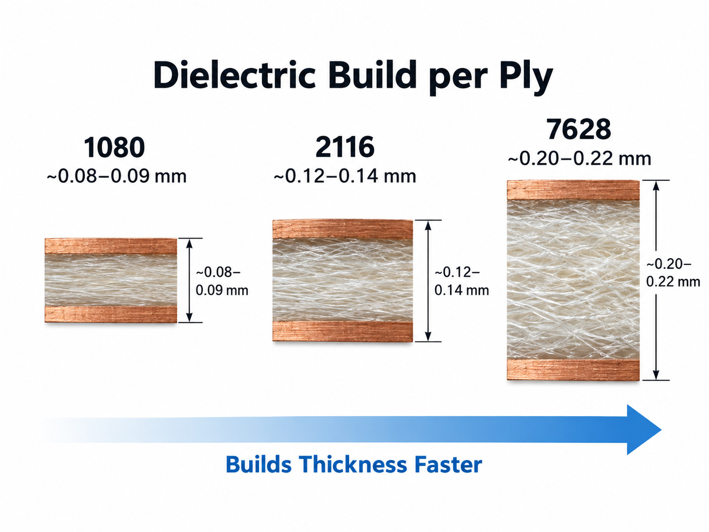
You may also like