A Tachyon 100G PCB manufacturer for a U.S. networking project needs to deliver a board that meets the specified stackup, HDI interconnect and electrical requirements. The material name alone cannot establish that fit. A thick backplane, a dense BGA line card and a short daughtercard can use the same laminate while presenting very different manufacturing challenges.
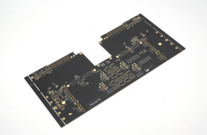
EBest Circuit (Best Technology) manufactures Tachyon 100G PCBs and supports PCB assembly, including a 20-layer HDI project for a U.S. customer developing 100G data-center networking equipment. That project combined controlled-impedance routing with dense BGA interconnects and passed the specified board-level inspections. To discuss a comparable build, send your stackup and fabrication files to sales@bestpcbs.com for a manufacturability review and quotation.
Which U.S. networking projects are a fit for Tachyon 100G?
Tachyon 100G is relevant to backplanes, daughtercards and high-layer-count line cards where dielectric loss consumes a significant part of the high-speed channel budget. For U.S. networking equipment developers, the strongest application fit is therefore a board with demanding signal paths, rather than every PCB installed in a data center.
Three project types illustrate the difference:
- Switch and router line cards: Dense BGA devices need escape routing and multiple signal layers. Material selection must work with the trace geometry that can actually fit between pads and vias.
- Equipment backplanes: Longer routes and connector transitions make channel attenuation and discontinuities important. A lower-loss dielectric helps with distributed trace loss; it does not remove losses or reflections at connectors and vias.
- High-speed daughtercards: A compact board can still be demanding when fine routing, layer transitions and closely spaced interconnects limit the available geometry.
Start with the intended channel, its length and its allowed loss. If an ordinary laminate already meets the electrical and manufacturing requirements with adequate margin, the equipment's 100G label alone is not a reason to change materials. Where dielectric loss is limiting the design, Tachyon 100G laminate and prepreg become relevant options to evaluate.
Which Tachyon 100G PCB manufacturers should U.S. buyers compare?
EBest Circuit, NetVia Group and Siber Circuits offer different starting points for a manufacturer comparison. Their locations and service focus matter because a U.S. customer may need domestic fabrication, an overseas production partner, or a supplier that coordinates both PCB manufacturing and assembly.
| Manufacturer | Location | Relevant Tachyon 100G experience or scope |
|---|---|---|
| EBest Circuit (Best Technology) | China | 20-layer Tachyon 100G HDI project for a U.S. customer; PCB fabrication and assembly support |
| NetVia Group | Dallas area, Texas, USA | Tachyon 100G fabrication, hybrid stackup engineering and RF coupon testing that includes insertion loss |
| Siber Circuits | Markham, Ontario, Canada | PCB fabrication using Isola Tachyon 100G for high-frequency and high-speed digital applications |
First resolve any requirement for the board to be manufactured in the United States. A Canadian or Chinese facility does not meet that geographic requirement simply by supplying a U.S. customer. Where overseas fabrication is acceptable, compare the specific board technology, test scope and shipment arrangements alongside price.
Next, match the difficult feature in your design. A manufacturer experienced with a simple Tachyon board may still need to qualify a thick HDI build or a mixed-material stackup. For loss-sensitive channels, establish whether the quotation includes only continuity and impedance checks or also the required transmission measurements. These distinctions make the comparison useful without treating one supplier as the best choice for every project.
Why can two Tachyon 100G PCB quotes specify different stackups?
Tachyon 100G identifies a material system, not one fixed dielectric construction. Two quotations can use that name while proposing different core thicknesses, prepreg constructions, resin contents or copper profiles. Those differences affect both the finished dimensions and electrical behavior.
For example, suppose two suppliers quote the same differential impedance target. One proposes a thicker dielectric between the signal layer and its reference plane. With other variables unchanged, the trace geometry must be adjusted to recover the target impedance. The result may require more routing space around a dense BGA, even though both quotations state the same nominal impedance.
The construction comparison should therefore connect each specification to its effect:
- Core and pressed prepreg thickness: Establish the signal-to-reference spacing used in the impedance calculation.
- Glass and resin construction: Determine which construction-specific dielectric values apply; a headline Dk is not a substitute for that selection.
- Copper profile and finished thickness: Affect conductor loss and the trace geometry remaining after fabrication.
- Trace width and pair spacing: Show whether the proposed impedance solution fits the released routing.
Approve a complete stackup with its corresponding geometry before comparing the final prices. Keep that construction with the production revision: a later change under the same material trade name can require a renewed impedance calculation or dimensional review.
When does a hybrid Tachyon 100G stackup make sense?
A hybrid stackup can make sense when only part of the board needs an ultra-low-loss dielectric. For example, a design may contain long high-speed channels alongside low-speed control circuitry. Selective use of Tachyon 100G can then be evaluated against using it throughout the board.
The selection must follow the electric field around each critical trace. An internal signal layer is influenced by the dielectric on both sides, so assigning one adjacent layer a low-loss material does not automatically give the complete transmission line the same behavior as an all-Tachyon construction.
There is also a manufacturing tradeoff. Different resin systems must tolerate a compatible bonding process, and their dimensional movement must be managed through lamination. Any material saving has to be weighed against qualification work, additional process constraints and possible yield effects.
A hybrid build is worth evaluating when critical channels can be clearly separated and the fabricator has experience with the proposed combination. A full Tachyon construction is usually simpler to specify when demanding signal paths occupy most routing layers or when an existing design has already been qualified on that construction. Neither option should be selected from laminate price alone.
What makes thick Tachyon 100G backplanes difficult to manufacture?
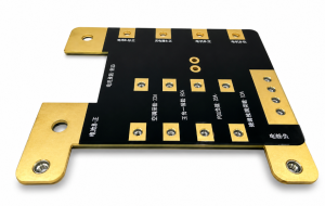
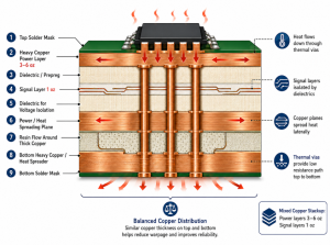
Thick backplanes combine long drilled holes with many layers that must remain aligned after lamination. Reducing the dielectric loss does not make those holes easier to drill or plate.
Hole geometry explains part of the difficulty. As a simplified comparison, a 3.0 mm board with a 0.30 mm drilled through-hole has a 10:1 thickness-to-drill-diameter ratio. Reducing that drill to 0.20 mm raises the ratio to 15:1. That deeper, narrower opening is more demanding for debris removal and plating access. These are illustrative calculations, not EBest process limits, and the drilled diameter must not be confused with the smaller finished plated opening.
Tachyon processing also requires drill conditions suited to the material. For thick, high-layer-count boards above 2.5 mm, the material's processing guidance recommends drilling one board high as a starting point. That can reduce throughput compared with drilling several boards together.
Registration creates a separate challenge. Laminate movement during processing varies with construction and grain direction. A compensation setting that worked on a thinner board cannot automatically be transferred to a thick backplane. Relevant manufacturing experience therefore includes comparable thickness, hole geometry and layer construction, rather than layer count alone.
Do impedance test results also prove low insertion loss?
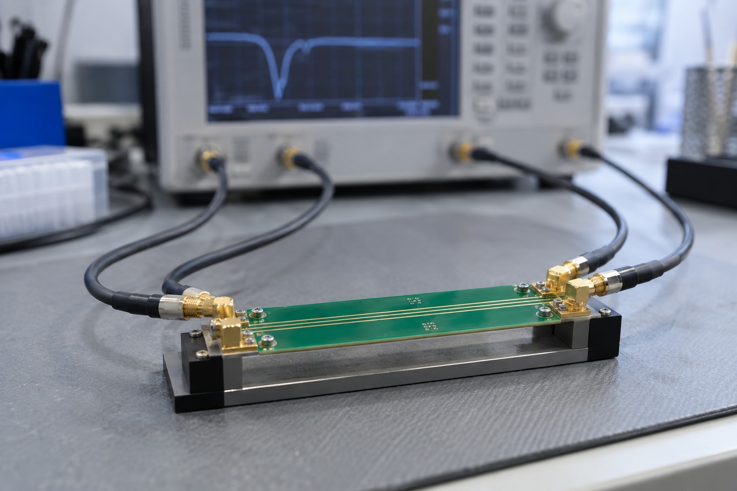
No. An impedance-only report does not establish the channel's insertion loss. TDR impedance measurements show how the measured structure compares with its impedance target. Insertion loss measures how much of the signal is transmitted through the structure across frequency.
Two traces can meet the same impedance specification while having different attenuation because of their length, dielectric or copper surface profile. Likewise, a board can pass continuity testing while still having an unsuitable high-frequency channel.
Match the acceptance question to the measurement:
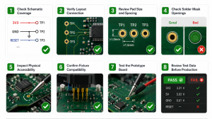
- Electrical continuity and isolation testing: Checks the board for opens and shorts against the test requirements.
- TDR impedance verification: Checks the impedance of the measured traces or representative coupons against the specified tolerance.
- Insertion-loss measurement: Evaluates transmission over the required frequency range; differential channels are commonly characterized with differential transmission data such as SDD21.
- Microsection inspection: Examines sampled internal structures, including plating and interconnections, rather than the complete channel's operating performance.
Where loss is a release criterion, agree on the coupon construction, measurement bandwidth and acceptance limit before fabrication. The coupon must represent the relevant routing construction, and test launches must be accounted for. Board-level measurements then support the equipment team's channel validation; they do not replace testing with the actual connectors, devices and operating configuration.
When is combined Tachyon PCB fabrication and assembly useful?
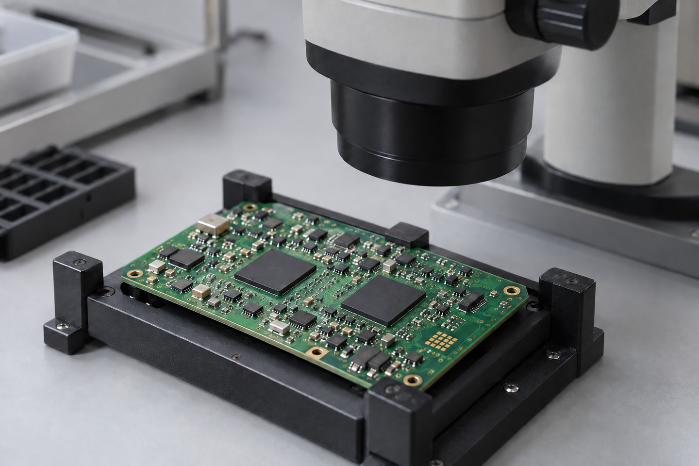
Combined fabrication and assembly is useful when the board's HDI details directly affect component attachment. A fine-pitch BGA is a clear example: its escape routing may require via-in-pad features, while its solder joints need suitable pad surfaces and a controlled assembly process.
An open via in a soldering pad can draw solder away from the joint. Where the design requires filled and capped vias, that condition must be delivered by the bare-board process before assembly begins. Discovering the mismatch at stencil printing is too late to solve it through a placement adjustment.
Coordinating Tachyon PCB fabrication and assembly allows the pad, via-fill, surface-finish and panel requirements to be reviewed together. EBest Circuit supports both stages, giving a project team one route for resolving these manufacturing interfaces.
Separate sourcing remains practical when a qualified assembler is already responsible for the product and the incoming-board requirements are settled. In either arrangement, keep acceptance scopes distinct: a bare-board electrical test checks the PCB network; assembly inspection and functional testing address the populated board. Functional testing requires the customer's test procedure and any necessary fixtures or software.
How Did EBest Circuit Build a Tachyon 100G PCB for a U.S. Customer?
EBest Circuit manufactured a 20-layer Tachyon 100G HDI PCB for a U.S. customer developing 100G data-center networking equipment. The design used high-speed SerDes transmission and dense BGA interconnects, so the build had to combine controlled-impedance differential routing with manufacturable HDI connections.
| Project item | Specification or result |
|---|---|
| Board construction | 20-layer Tachyon 100G HDI PCB; 2.4 mm finished thickness, ±10% |
| Critical interconnects | Blind and buried vias, with via-in-pad features for dense BGA routing |
| Differential impedance | 100 ohms, ±10%; critical differential structures met the specified tolerance |
| Prototype production | Approximately 15–18 days |
| Production yield | Approximately 93%–95% for this project |
| Completed checks | 100% electrical testing, TDR impedance verification and microsection inspection passed |
Translating the layout into a buildable stackup
The customer supplied the layout, and EBest reviewed the stackup, drill files, impedance table and fabrication notes before production. The key issue was whether the proposed dielectric spacing and trace geometry could maintain the impedance target while preserving the dense BGA routing. Manufacturing proceeded against the approved production files, keeping the electrical requirements connected to the actual board construction.
Checking the HDI interconnections
Blind and buried vias provided connections between selected layers, while via-in-pad supported the compact BGA routing. EBest reviewed these features for manufacturability. Microsection inspection passed, supporting acceptance of the inspected plating and interconnection structures. This complemented the electrical test, which checked continuity and isolation rather than exposing the internal copper geometry.
Verifying the prototype outcome
Prototype production was completed in approximately 15–18 days, with production yield around 93%–95%. The finished boards passed 100% electrical testing and TDR verification, and the critical differential structures remained within the specified impedance tolerance. These results gave the customer a verified bare-board foundation for subsequent assembly and equipment validation.
The schedule and yield describe this project; they are not standard promises for every 20-layer order. For a similar design, EBest can review the actual stackup, HDI structure and test requirements to establish the manufacturing scope and quotation. U.S. shipment timing should be confirmed separately from prototype production time.
FAQs About Choosing a Tachyon 100G PCB Manufacturer
Does Isola manufacture the finished Tachyon 100G PCB?
Isola produces the laminate and prepreg. A PCB fabricator converts those materials into the finished circuit board through imaging, etching, lamination, drilling, plating and inspection. Confirm both the material identity and the company responsible for fabrication.
Does Tachyon 100G mean every signal lane operates at 100 Gb/s?
No. The material name does not define the equipment's lane rate, modulation or channel length. Suitability depends on the complete interface requirements and the losses and discontinuities along its signal path.
Can another low-loss laminate replace Tachyon 100G without changing the design?
Not automatically. A replacement can change dielectric behavior, copper options, pressed thickness and processing conditions. It needs engineering approval against the actual construction and channel requirements, even when its headline Dk or Df looks similar.
Can the prototype production time be used as the U.S. delivery date?
No. Production completion and delivery are different milestones. Confirm whether the quoted schedule includes testing, any assembly, dispatch, transit and import clearance before using it in the equipment build plan.
What should a U.S. customer send for an initial quotation?
Provide Gerber and drill files, the intended stackup, impedance targets and tolerances, quantity, and the required PCB completion date. Include any insertion-loss acceptance requirement. For assembly, add the BOM, placement data and assembly drawing so the supplied scope can be quoted accurately.
Looking for a Tachyon 100G PCB manufacturer for your next U.S. project? Send your board files and required build quantity to sales@bestpcbs.com. EBest Circuit can review the manufacturing fit, identify stackup or HDI issues that need resolution, and prepare a quotation for bare-board fabrication or a coordinated PCB and assembly build.