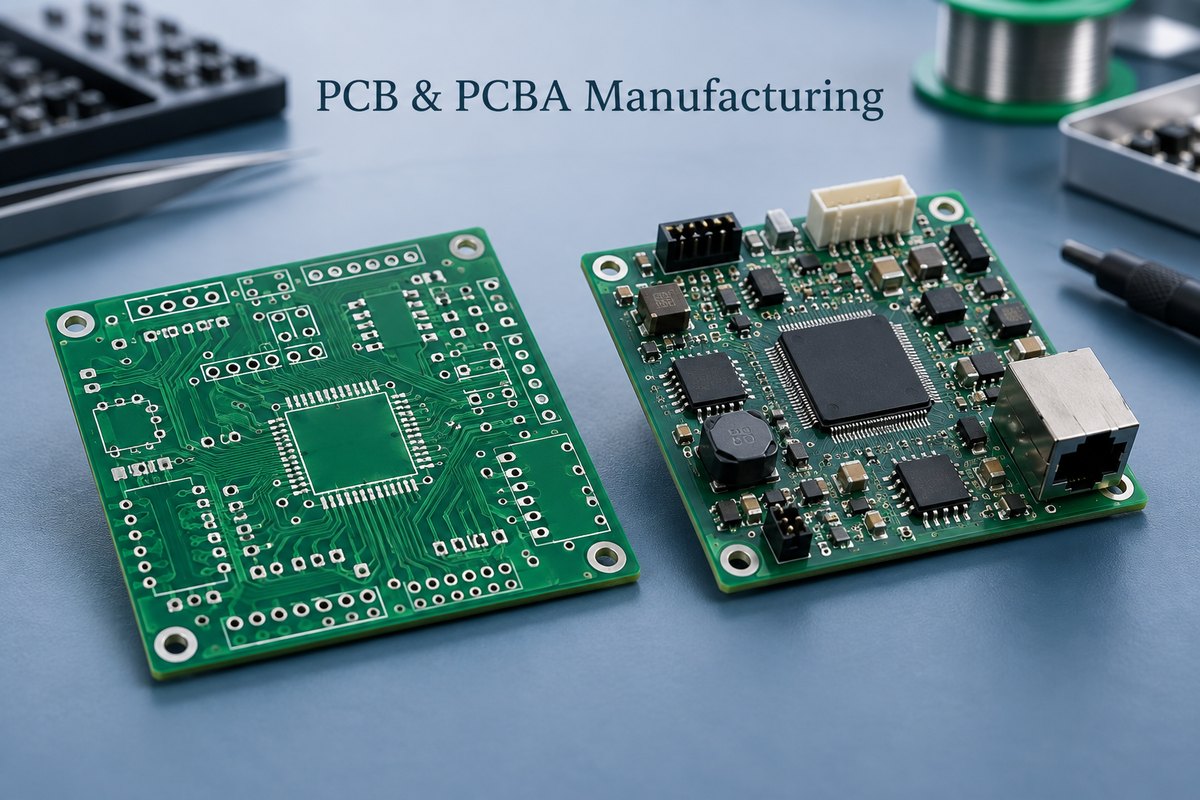
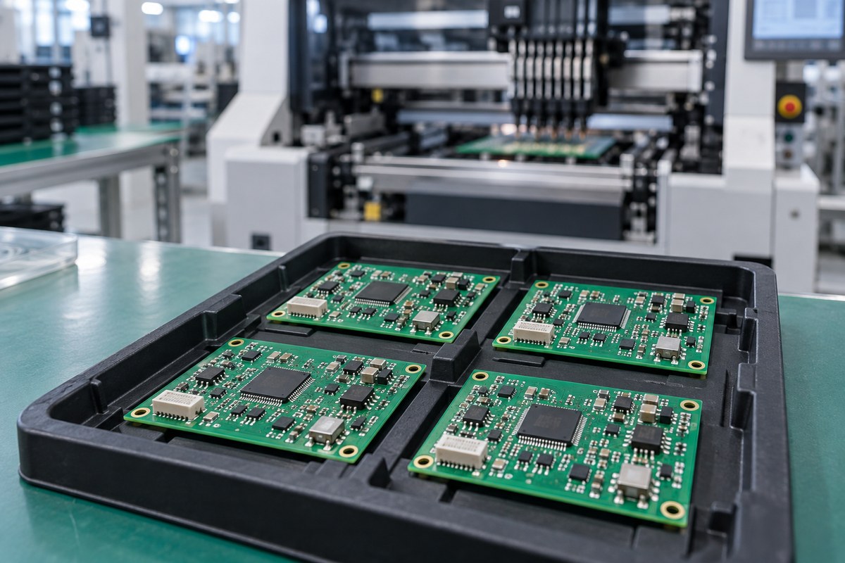
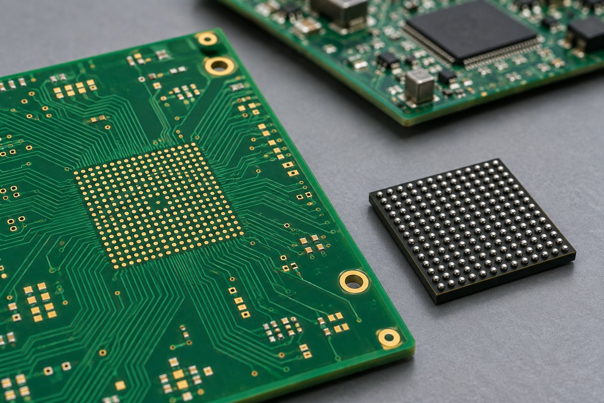
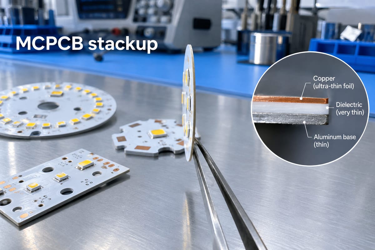
OAM PCB is the accelerator-module circuit board used to connect high-density AI compute with a server's power, high-speed links, management, and cooling systems. OAM means OCP Accelerator Module; the module normally works with a Universal Base Board (UBB) rather than operating as a stand-alone processor board. This guide shows how the parts fit together, how OAM differs from SXM, and which electrical, thermal, mechanical, fabrication, and assembly requirements matter to a buyer.
EBest Circuit (Best Technology) supports AI accelerator PCB projects with high-layer and HDI fabrication, controlled impedance, component sourcing, BGA assembly, AOI, X-ray inspection, and customer-defined test coordination. If you are evaluating an OAM PCB, send your current board requirements to sales@bestpcbs.com for an initial manufacturability discussion.
OAM accelerator PCB module in an AI server platform.
What Is an OAM PCB?
An OAM PCB is the printed circuit board used in an OCP Accelerator Module. It carries an AI accelerator device and the supporting circuitry required to power, manage, connect, and cool that device inside a compatible server platform.
Compute: a GPU, ASIC, NPU, FPGA, or another parallel processor.
Local support: memory, voltage regulation, clocks, management devices, and sensors.
System connection: the connector and mechanical interfaces that link the module to a compatible baseboard and cooling assembly.
OAM defines a form factor and interface framework, not a processor brand or a fixed PCB construction. The actual layer count, materials, vias, components, and tests still depend on the accelerator, power envelope, cooling approach, UBB, and product specification.
How Does an OAM PCB Work in an AI Server?
Inside an AI server, the OAM PCB acts as the local platform for one accelerator. It receives power and management connections from the system, provides the short electrical paths needed around the accelerator and memory, and connects high-speed links to the UBB.
The UBB brings multiple OAM modules together. It distributes power and management signals and provides the physical interconnect fabric between accelerators. Depending on the system architecture, those accelerator-to-accelerator links can support the very high data movement needed for training or inference workloads.
A simplified data path is:
The host server sends work and data toward the accelerator platform.
The UBB routes high-speed links, power, and control connections to each OAM module.
The OAM PCB supports the accelerator, local memory, power conversion, sensing, and module-level interfaces.
Cooling hardware removes heat from the accelerator and other high-power components.
This division lets the module, baseboard, host, power system, and cooling system be developed as coordinated building blocks. It also means an OAM PCB cannot be evaluated in isolation: its connector geometry, mounting features, power inputs, thermal stack, and high-speed interfaces must match the intended platform.
What Does the OAM Architecture Include?
Although implementations vary, the OAM architecture normally combines several functional groups on one dense PCB.
Accelerator package: the main GPU, ASIC, NPU, FPGA, or other compute device.
Local memory: high-bandwidth or other memory devices placed close to the accelerator when required by the processor architecture.
Power delivery: voltage regulators, inductors, capacitors, current sensing, and power-control circuits that convert the module input into multiple low-voltage rails.
High-speed interfaces: differential channels connecting the accelerator to other modules, the host, and management resources through the module connector.
Management and monitoring: controllers, EEPROMs, clocks, temperature sensors, voltage monitors, and service interfaces.
Mechanical and thermal interfaces: mounting holes, keep-out areas, stiffeners, heatsink contact zones, and the flatness needed for reliable connector engagement and cooling contact.
These groups compete for board area and influence one another. A larger power stage changes copper distribution and thermal behavior. Dense high-speed escape routing can require HDI structures. A heavy heatsink can increase mechanical loading. The architecture must therefore be translated into one coordinated stackup, layout, fabrication, assembly, and cooling plan.
How Do OAM Modules and UBBs Work Together?
An OAM module is the accelerator board; a UBB is the baseboard that hosts and connects multiple modules. The two boards perform different jobs but operate as one platform.
Platform part
Primary role
What must match
OAM module
Carries one accelerator and its local support circuits.
Connector, power, lane map, cooling, and mounting.
UBB
Hosts and links multiple OAM modules.
Sockets, routing, current capacity, management, and clearances.
AI server
Combines compute, power, cooling, firmware, and software.
Power sequence, thermal capacity, service access, and validation.
A useful way to picture the relationship is: AI server -> UBB -> multiple OAM modules -> accelerator and local memory on each module.
For example, when eight accelerator modules are installed on one UBB, a connector-position error on one OAM PCB can prevent reliable mating, while an incorrect lane map or channel-loss assumption can affect communication beyond that single module. The OAM and UBB suppliers therefore need controlled interface drawings and the same revision baseline.
Eight OAM modules connect through a UBB inside an AI server tray.
OAM vs SXM: What Is the Difference?
OAM and SXM are both used for high-performance accelerator modules, but they come from different platform ecosystems. OAM is associated with the Open Compute Project and is intended to support an open, multi-vendor infrastructure. SXM is a proprietary NVIDIA module format used in selected NVIDIA server platforms.
Decision area
OAM
SXM
Ecosystem
Open, OCP/OAI-oriented.
Proprietary NVIDIA platform.
Choose when
The system uses an OAM-compatible accelerator and UBB.
The selected NVIDIA platform requires SXM.
Baseboard
OAM-compatible UBB.
Designated NVIDIA baseboard.
Can they swap?
No; the complete platform must match.
The two formats should not be treated as drop-in replacements. Moving a design from one to the other can affect the module PCB, baseboard, firmware, cooling assembly, power delivery, chassis, and system validation. The form-factor decision belongs at the platform architecture stage, before PCB fabrication data is released.
What Are the PCB Design Requirements for OAM-Compatible Systems?
An OAM-compatible system must carry fast signals, high current, dense packages, and substantial thermal and mechanical loads at the same time. The PCB design requirements are therefore interconnected.
Stackup and materials must support the required channel loss, impedance, layer count, thickness, and fabrication capability.
Differential pairs need controlled geometry, continuous reference planes, suitable spacing, and a via strategy that limits discontinuities.
Large packages and dense connectors may require blind or buried vias, microvias, via-in-pad, filled vias, and back drilling.
Power and ground structures must carry the module current while controlling voltage drop, noise, and localized heating.
Copper distribution and layer construction must support board flatness and reduce assembly warpage risk.
Connector footprints, mounting holes, heatsink interfaces, keep-outs, and board edges must follow the mechanical definition of the target platform.
The most useful design review looks at the complete path: accelerator package breakout, on-module routing, connector launch, UBB routing, and the destination device. A locally correct trace can still fail if the combined channel exceeds its loss or discontinuity budget.
What Power and Thermal Requirements Shape an OAM PCB?
OAM PCBs combine high power density with strict mechanical and signal-integrity requirements. Power and thermal design therefore shape the physical PCB, not just the component selection.
Requirement group
What shapes the PCB
What the customer must define
Power
Planes, copper, vias, decoupling, and regulator layout.
Input power, rail current, voltage drop, transients, and sequence.
Thermal
Heat spreading, component spacing, and cooler interface.
Cooling method, contact area, temperature limits, and test conditions.
Mechanical
Thickness, stiffeners, mounting, alignment, and flatness.
Datums, mounting load, keep-outs, tolerances, and tray limits.
These requirements must be reviewed together. More copper may improve current capacity but can change etching, lamination, impedance geometry, flatness, and reflow behavior. A large cooling assembly may remove heat effectively but still create board strain if the mounting stack is not coordinated.
The PCB manufacturer can review manufacturability and material implications, but final power integrity, cooling design, and server validation remain system responsibilities.
How Are PCBs Fabricated and Assembled for OAM Modules?
OAM modules are commonly advanced multilayer assemblies, but the exact process should follow the released design rather than a generic OAM recipe.
Fabrication review: confirm materials, copper, impedance geometry, via structure, lamination, registration, back drilling, thickness, flatness, and finish.
Assembly planning: account for large BGAs, memory, power components, connector coplanarity, thermal mass, moisture control, paste, placement, and reflow.
Verification plan: select bare-board electrical test, impedance testing, SPI, AOI, X-ray, dimensional checks, and customer-defined functional tests according to the real risks.
No single inspection method proves the whole module. The evidence plan should match the likely failure modes and the test points that are actually accessible.
EBest Circuit (Best Technology) can support manufacturability review, material coordination, PCB fabrication, component sourcing, BGA assembly, AOI, X-ray inspection, and customer-defined testing coordination. Accelerator architecture, firmware, system cooling, regulatory compliance, and final server qualification remain with the customer and its platform partners.
Inspection of a high-density OAM PCB assembly in an electronics laboratory.
Where Is OAM PCB Technology Used?
OAM PCB technology is used where systems need dense, modular accelerator computing. The most visible applications are AI training servers and high-performance computing platforms, but the same infrastructure can also support inference, data analytics, scientific computing, and other workloads built around compatible accelerator modules.
AI training servers that need several tightly connected accelerator modules.
High-performance computing clusters handling scientific or engineering workloads.
Cloud and enterprise AI infrastructure designed around serviceable accelerator trays.
Inference and data-analytics platforms that benefit from dense modular compute.
Specialized compute appliances built around an OAM-compatible accelerator ecosystem.
OAM is not automatically the best format for every AI product. PCIe cards may be simpler for lower-power or broadly compatible add-in acceleration, while embedded modules may fit edge systems with tighter space and power limits. OAM becomes most relevant when the platform benefits from high accelerator density, strong module-to-module communication, serviceable modular hardware, and coordinated power and cooling.
How to Choose an OAM PCB Manufacturer?
An OAM PCB manufacturer should be evaluated against the released board requirements, not against a generic list of advanced capabilities.
Evaluation stage
What to confirm
Why it matters
1. Platform fit
Understands the OAM/UBB interface and board requirements.
Prevents interface assumptions from reaching production.
2. Process fit
Covers the required HDI, impedance, assembly, and inspection steps.
Keeps fabrication and assembly decisions aligned.
3. Build control
Controls material, stackup, BOM, files, and test revisions.
Reduces prototype-to-production revision drift.
The best supplier is not necessarily the one that claims the highest layer count. It is the one that can explain how the specific OAM design will be built, where its process margins are tight, what evidence will be delivered, and which responsibilities remain with the system developer.
For project-specific review, send the released Gerber or ODB++ data, stackup, fabrication drawing, BOM, placement data, assembly drawing, connector and mechanical definitions, and test requirements to sales@bestpcbs.com.
FAQs About OAM PCB
What does OAM mean in PCB hardware?
OAM means OCP Accelerator Module. In PCB hardware, it describes an accelerator-module form factor and interface framework developed in the Open Compute Project ecosystem.
Is an OAM PCB the same as a UBB?
No. The OAM PCB carries one accelerator module. The Universal Base Board hosts and connects multiple OAM modules and provides shared interconnect, power, management, and mechanical integration.
Is OAM the same as NVIDIA SXM?
No. Both are accelerator-module formats, but OAM belongs to an open OCP/OAI ecosystem while SXM is a proprietary NVIDIA platform. Their interfaces and system requirements are not interchangeable.
Why are OAM PCBs difficult to manufacture?
They can combine high layer counts, low-loss materials, HDI vias, dense high-speed routing, high-current power structures, large BGA packages, strict flatness, and demanding thermal hardware on one assembly.
What should be reviewed before building an OAM PCB?
Review the platform specification, board and UBB revisions, stackup, impedance and loss targets, via structure, power inputs, connector and mechanical definitions, thermal stack, BOM, assembly data, and inspection and test requirements.
Planning an OAM PCB or another AI accelerator PCB? Send your current design package or project questions to sales@bestpcbs.com. EBest Circuit (Best Technology) can review the PCB fabrication, sourcing, assembly, inspection, and customer-defined test scope for your build.
A driver monitoring IR LED aluminum PCB provides the near-infrared illumination that helps an automotive DMS camera capture the driver’s face and eyes in changing cabin light. For buyers, the right board is not simply an aluminum PCB populated with IR LEDs. Its optical position, pulse-current path, heat flow, camera compatibility, assembly controls, and verification plan must work as one module.
When the PCB manufacturer receives the pulse profile, LED data, mechanical drawing, optical datums, thermal limits, and test expectations before quotation, it can identify missing production inputs before they become tooling changes, assembly delays, or inconclusive prototype results.
Are you worried about your driver monitoring IR LED aluminum PCB project?
Will uneven IR coverage leave the driver’s eyes underexposed at off-axis seat positions?
Could pulse-current droop or trigger delay reduce usable illumination during camera exposure?
Will an incomplete board-to-housing heat path raise LED temperature during repeated pulses?
With over 20 years of experience, EBest Circuit provides one-stop PCB and PCBA manufacturing support from prototype review through production.
Optical datum review: We check LED position, rotation, board outline, and mounting references against the supplied camera and housing drawings before fabrication.
Pulse-path review: We review the supplied peak current, pulse width, trigger timing, copper path, return path, and assembly inputs before prototype release.
Thermal-interface review: We check the specified aluminum construction, dielectric, board flatness, mounting pattern, and housing-contact requirements against the released manufacturing package.
Ready to start your driver monitoring IR LED aluminum PCB project? Send your files and requirements to sales@bestpcbs.com.
What Does a Driver Monitoring IR LED Aluminum PCB Do in an Automotive DMS?
A driver monitoring IR LED aluminum PCB supports the IR emitters electrically, thermally, and mechanically so the DMS camera can obtain usable images of the driver. The board carries pulse current to the LEDs, transfers heat toward the aluminum base and housing, and holds the emitters at controlled locations relative to the camera and lens.
A driver monitoring system IR LED board therefore sits at the intersection of several project teams. The electronics team defines current and timing. The optical team defines wavelength, beam shape, coverage, and camera alignment. Mechanical engineers control the board position and heat-transfer interfaces. Manufacturing and quality teams convert those inputs into repeatable assembly and acceptance evidence.
Project Input
PCB or PCBA Decision
Business Risk If Missing
Camera exposure timing
Pulse trigger and current-delivery requirements
Prototype images may be too dark, inconsistent, or affected by switching
LED electrical and thermal data
Driver headroom, copper path, dielectric, and heat path
Redesign after component selection or thermal testing
Optical and mechanical datums
LED footprint position, board outline, and assembly orientation
Illumination may miss the required face or eye region
Vehicle and customer requirements
Materials, controls, traceability, and test planning
Quotation may exclude required verification or documentation
Use this matrix to assign each missing input to the responsible team before quotation. Camera timing belongs with the electronics and imaging teams, optical datums with optical and mechanical engineering, and verification records with the customer, module owner, and supplier according to the agreed scope.
How Do IR LEDs Provide Consistent Illumination Across the Driver’s Face and Eyes?
Consistent illumination comes from coordinating LED position, emission angle, lens behavior, camera axis, and the expected driver-position range. Increasing LED power cannot correct a beam that is aimed at the wrong region or blocked by the steering wheel, trim, or eyewear reflections.
For an automotive DMS IR illuminator, the PCB drawing should identify optical and mechanical datums rather than relying only on the board outline. LED pad locations, polarity, rotational orientation, component height, and permitted placement variation can all influence the final beam. The optical validation plan should also include realistic driver positions, eyeglasses or sunglasses where applicable, and the actual camera-lens stack.
Define the coverage zone: specify the face and eye region at the required seat travel, seat height, steering-wheel position, and driver posture. This prevents the optical target from being reduced to one nominal head position.
Lock optical datums: dimension LED centers and rotation from mounting features that also locate the camera, lens, PCB, and housing. Board-edge tolerances are insufficient when the enclosure uses different functional references.
Match the beam to the FOV: compare the LED radiation pattern and any secondary optics with the camera field of view. Overly wide illumination wastes current outside the captured region; a narrow or misaligned beam creates dark areas as the driver moves.
Review obstruction and reflection risks: evaluate trim, steering-wheel position, eyeglasses, sunglasses, bright facial reflections, and off-axis viewing. These conditions can hide the eyes even when total scene brightness appears adequate.
Validate the assembled module: capture images through the production-intent lens, filter, cover window, and housing across the required driver positions. A bare-board radiometric measurement cannot establish image uniformity after the optical stack is installed.
Record both the operating condition and the image result. LED current, exposure, ambient light, seat position, eyewear, and module temperature should be traceable to each validation image so that an optical problem can be separated from a timing, thermal, or assembly change.
How Are IR LED Pulses Synchronized with DMS Camera Exposure?
Use the camera’s exposure or strobe signal to command the LED driver, then place the full IR current pulse inside the pixels’ light-collection period. The timing budget must include trigger propagation, driver turn-on delay, current rise and fall time, and worst-case tolerance. If either edge falls outside the exposure interval, part of the optical pulse produces heat without contributing to the captured image.
Shutter type changes the synchronization decision. A global-shutter sensor exposes all pixels together, so one pulse can cover the shared exposure interval. A rolling-shutter sensor exposes rows at different times; a short pulse may illuminate only part of the frame unless the sensor provides a supported strobe mode or the pulse covers the required row sequence. Confirm the method in the selected image-sensor documentation before fixing the PCB trigger interface.
Timing Check
What to Establish
Failure Visible in the DMS Image
Trigger reference
Which camera or controller edge starts the illumination command
Pulse occurs in the wrong frame or at an inconsistent phase
Driver delay
Delay from the logic command to stable LED current, including tolerance
Reduced effective illumination or frame-to-frame brightness change
Pulse window
Start and end margins inside the applicable global or rolling exposure period
Dark rows, uneven exposure, or wasted on-time
Repetition behavior
Current recovery and timing stability across the required frame sequence
Brightness changes during consecutive frames
Fault limit
Maximum on-time and the shutdown response if the trigger remains active
Excess heat or optical output outside the intended operating state
During prototype validation, observe the trigger and LED current on the same time base while the camera captures images. Repeat the check at the specified supply and temperature limits; a waveform that aligns at room temperature alone does not establish the available timing margin.
How Does the PCB Handle High Peak Current During IR LED Pulses?
The PCB must deliver the specified peak current without excessive voltage drop, unstable driver operation, or unwanted disturbance elsewhere in the module. This depends on the complete current loop, not only the nominal copper thickness.
The design review should follow current from the local energy source through the driver, LED string, return path, and decoupling network. Trace geometry, copper weight, connection transitions, component placement, voltage headroom, and recharge time all affect the result. The driver and LED datasheets remain the authority for component limits; the PCB supplier should not replace missing electrical specifications with assumed universal values.
Review Item
Decision Needed
Evidence for Prototype Approval
Pulse profile
Peak current, width, frequency, duty cycle, and tolerance
Measured waveform at the defined operating condition
Voltage headroom
Supply range, LED string voltage, driver losses, and transient margin
Waveform remains within selected component limits
Current loop
Short routing, return continuity, connections, and local storage
No unexpected droop, overshoot, or unstable pulse shape
Recharge interval
Energy replenishment before the next exposure
Repeated pulses remain consistent over the required sequence
Release the pulse-current design for prototype testing only after the measured waveform confirms the required peak current, timing, voltage headroom, and recovery between exposures. If one result is outside its limit, correct the current loop or operating specification before using thermal or optical results as approval evidence.
How Is Heat Controlled for Pulsed IR LEDs on an Aluminum PCB?
Thermal control requires a continuous heat path from the LED junction through the package, PCB, aluminum base, interface material, and housing. An aluminum substrate helps spread heat, but it does not by itself prove an acceptable junction temperature or service life.
Peak LED power affects the temperature rise during each pulse, while duty cycle, repetition rate, driver losses, ambient temperature, and the module’s thermal time constants determine accumulated heating. Review peak conditions for component limits and average dissipation for the sustained thermal state; using only one of them can hide a different failure mode.
Start with the real pulse profile: use LED forward voltage, peak current, pulse width, repetition rate, and worst permitted on-time. Include driver and resistor losses when they share the same board and heat path.
Review the dielectric layer: thermal conductivity and dielectric thickness act together. A high-conductivity material can still create excessive thermal resistance if the construction or bond line is too thick for the required heat flow.
Spread heat before the bottleneck: size LED pads and connected copper so heat reaches the dielectric over a practical area. Narrow copper necks can limit spreading before heat reaches the aluminum base.
Complete the housing interface: define board flatness, mounting pressure, interface material, contact area, fastener pattern, and housing surface. Air gaps or uneven contact can dominate the module result even when the PCB construction is correct.
Check the hottest operating case: combine the highest permitted ambient, pulse sequence, enclosure condition, and heat from nearby components. Test the location expected to run hottest rather than relying on a convenient board-edge measurement.
Prototype approval should link a temperature measurement at a defined location to the LED junction through the package manufacturer’s thermal data and an agreed calculation or model. Record the ambient condition, pulse sequence, stabilization time, sensor position, interface assembly, and acceptance limit. External board temperature alone does not prove junction temperature, optical-output stability, or LED life.
How Does PCB Layout Prevent Switching Noise from Affecting the DMS Camera?
Layout reduces interference by shrinking fast-current loops, controlling return paths, and separating switching nodes from sensitive camera and data circuits. Filtering cannot fully compensate for poor current-loop geometry.
Close the pulse-current loop: place the driver, local energy-storage capacitor, LED connection, current-sense element, and power return close enough to avoid a large high-di/dt loop. Long paths increase voltage disturbance and radiated coupling.
Control the switching-node area: keep high-dv/dt copper no larger than required and away from camera, clock, trigger, and communication routing. Do not route sensitive traces under or beside an exposed switching region without an intentional reference structure.
Preserve return continuity: provide a defined path for pulse current and a stable reference for camera and data signals. A split or narrow return path can force current through a shared reference and convert switching current into image or communication noise.
Place filtering at the disturbance boundary: locate local decoupling at the driver and any interface filtering where power or signals enter the sensitive region. A filter placed after a long noisy trace leaves the coupling path intact.
Protect trigger integrity: route the exposure or strobe signal away from the power switch node, control its return path, and check logic thresholds at the receiving pin. Trigger jitter or false edges can look like an optical-timing problem.
Balance edge rate and optical timing: slew-rate control may reduce emissions, but a slower current edge consumes timing margin and can reduce useful optical energy during a short exposure. Verify both waveform quality and captured images after changing the edge rate.
PCB review can identify layout risk, but vehicle EMC compliance requires the applicable module and vehicle tests. During prototype work, monitor electrical emissions, trigger integrity, data communication, and camera images under the same representative pulse modes; a continuity test cannot reveal exposure-related coupling.
What Automotive Design Requirements Must Be Defined Before Layout Begins?
The project should define electrical, environmental, optical-safety, mechanical, quality, and traceability requirements before the PCB is released. This prevents a supplier from quoting a board that is manufacturable but incomplete for the intended automotive module.
Electrical envelope: document normal and abnormal supply conditions, pulse-current limits, trigger logic, load-dump or transient protection ownership, reverse-polarity strategy, and fault shutdown behavior. Identify which protections are on the illuminator board and which remain elsewhere in the module.
Environmental conditions: define operating and storage temperature ranges, temperature ramp or cycling conditions, vibration, mechanical shock, humidity or condensation exposure, coating needs, and installation loads. Connect each condition to the required board material, component grade, attachment method, or validation owner.
Optical-safety boundary: assign responsibility for the exposure assessment and provide wavelength, radiant-output data, pulse current, pulse width, repetition rate, lens or diffuser behavior, viewing geometry, and fault-state on-time. A component rating cannot replace the assembled optical-system assessment.
Mechanical interface: release the mounting datums, board outline, keep-outs, connector location, allowed warpage, housing contact area, interface material, fastener constraints, and permissible component height. These inputs control both optical alignment and the heat path.
Quality and change control: state applicable customer specifications, workmanship criteria, approved component sources, substitution rules, first-article expectations, process-change notification, lot traceability, retention period, and required reports.
Verification ownership: identify what is accepted by component documentation, bare-board inspection, assembled-PCB test, optical-module validation, EMC testing, environmental testing, and vehicle approval. Assign the pass criterion and evidence owner for each level before purchase-order release.
Convert the requirements into a responsibility matrix with four fields: requirement, applicable condition, acceptance evidence, and responsible organization. Request certification or material declarations by exact scope. A supplier management-system certificate, a material listing, a component rating, and a finished-module compliance result are different evidence types and cannot substitute for one another.
How Is a DMS IR LED Aluminum PCB Manufactured and Assembled?
Production should preserve the electrical, thermal, optical, and polarity decisions established during design review. The build route therefore needs controlled material identity, PCB fabrication, component orientation, reflow, cleaning, and traceability rather than a generic aluminum-board process description.
Confirm production inputs: release the approved fabrication data, stackup, aluminum and dielectric requirements, BOM, centroid file, polarity drawing, optical datums, panel requirements, and acceptance plan; record unresolved discrepancies before tooling.
Verify incoming materials: match laminate, dielectric construction, aluminum base, copper, surface finish inputs, LEDs, drivers, and assembly materials to the released documentation; quarantine mismatches to prevent an unapproved substitution.
Fabricate the PCB: image and etch the circuit, process the metal-core construction, drill or route required features, apply solder mask and surface finish, and control the board outline and datum features needed by the housing.
Prepare solder paste: use the approved stencil and printing setup for the selected LED and driver packages; inspect deposits where solder volume can affect coplanarity, thermal contact, or bridging risk.
Place components: load the released program and verify LED polarity, rotation, package identity, and datum-related placement before the batch proceeds to reflow.
Reflow and clean: use a profile compatible with the components, PCB construction, solder paste, and product requirements; review for package movement, void-related concerns where specified, contamination, and visible heat damage.
Depanel and identify: separate boards without damaging the aluminum structure or critical edges, then preserve lot and material traceability through inspection and shipment.
Build prototypes with the intended production materials and assembly orientation. If a temporary component or process is unavoidable, document the difference so the prototype result is not mistaken for production validation.
How Is a Driver Monitoring IR LED Aluminum PCB Inspected and Tested?
Inspection should produce evidence that the delivered board matches the released design and performs under the agreed test conditions. The plan should distinguish bare-board, assembled-board, module, and vehicle-level responsibilities.
Inspect the bare board: verify dimensions and specified datums, visual workmanship, electrical continuity and isolation, and the agreed material or traceability records; disposition deviations against the released drawing.
Inspect the assembly: confirm component identity, polarity, rotation, placement, solder joints, cleanliness, and mechanical condition using the agreed visual, AOI, or other inspection methods.
Measure the pulse: operate the assembly at defined supply and trigger conditions, measure current and relevant node waveforms, and compare peak value, width, timing, droop, and overshoot with approved limits.
Check thermal behavior: run the stated pulse sequence and ambient condition, measure at documented locations, and compare results with the project limit and junction-temperature assessment method.
Verify optical alignment: install the board in the representative optical-mechanical stack, capture camera output across the required driver positions, and assess coverage, reflections, and image consistency against system criteria.
Evaluate interference: operate worst-case pulse modes while monitoring camera images and data communication; escalate abnormal artifacts or errors for module-level EMC investigation.
Release the evidence: link results, nonconformance dispositions, lot identity, and approved deviations to the shipped samples or production batch so procurement can audit what was actually accepted.
What Should You Send for a DMS IR LED Aluminum PCB Quote?
The quotation package must define the board, assembly, control, and verification scope to be priced. Sending only Gerber files and quantity may produce a preliminary board price, but it cannot define optical alignment, pulse testing, component sourcing, or automotive documentation.
PCB data: Gerber or ODB++, drill files, outline, drawing, stackup, copper, dielectric, aluminum-base, surface-finish, and panel requirements.
Assembly data: BOM with manufacturer part numbers, centroid file, drawings, LED polarity and rotation, acceptable substitutions, and special handling needs.
System interfaces: camera and trigger information, pulse profile, supply range, connector details, optical datums, housing interface, and thermal limits.
Quality scope: inspection criteria, test limits, sample size, traceability, reports, customer specifications, and required declarations.
Commercial scope: prototype and production quantities, target schedule, delivery destination, packaging, and whether component sourcing or turnkey PCB assembly is required.
If some inputs are not yet frozen, identify them as open items. An early design review can separate information needed for budgetary pricing from information required before fabrication, assembly, or test release.
Why Choose EBest Circuit for Driver Monitoring IR LED Aluminum PCB Manufacturing?
EBest Circuit can support the project from PCB design review and prototyping through component sourcing, PCB assembly, and mass production.
Our supplied company information identifies metal-core PCB capability and services covering PCB design, PCB prototypes, mass production, component sourcing, and PCB assembly. It also lists an IATF 16949 certification within the company’s certification inventory. Certification relevance and document scope should be confirmed for the specific purchasing requirement rather than treated as automatic product approval.
Design-to-production continuity: review stackup, footprint, polarity, panel, sourcing, assembly, and test inputs before tooling. The same controlled package can then be updated through prototype findings instead of recreating requirements for each supplier handoff.
Metal-core project support: review the aluminum-PCB construction together with LED pad geometry, dielectric choice, board-to-housing contact, outline tolerances, assembly temperature exposure, and requested material evidence.
Prototype support: use sample builds to close placement, soldering, waveform, temperature, and optical-alignment questions. Record temporary materials or process differences so prototype evidence is not misapplied to production approval.
Component sourcing and assembly: coordinate approved manufacturer part numbers, alternates, LED bin or wavelength requirements when specified, polarity controls, placement data, and incoming records within the released BOM.
Production handoff: carry approved fabrication, assembly, inspection, and traceability requirements into mass production, with open deviations resolved before batch release.
Quotation clarity: separate budgetary assumptions from fabrication-release and test-release inputs, allowing procurement to compare quotations on the same technical scope.
Send the available design package even if the project is still at the prototype stage. We can review which inputs are sufficient for quotation and which must be completed before manufacturing release.
FAQs About Driver Monitoring IR LED Aluminum PCBs
Q1: Should a DMS use 850 nm or 940 nm IR LEDs?
A1: 850 nm often provides stronger response from a silicon image sensor, but the emitter may show a faint red glow. At 940 nm, the illumination is less noticeable to occupants, while the selected sensor and optical filter may require a different current or exposure budget. Compare LED radiant output, sensor response, filter transmission, image quality, and the optical-safety assessment at the same wavelength before selecting the emitter.
Q2: When is an aluminum PCB preferable to FR4 for a DMS illuminator?
A2: Choose an aluminum PCB when the emitter board needs a short heat-spreading path into a metal housing and the circuit can be routed within the available metal-core construction. FR4 may suit a board that needs dense multilayer routing or combines more camera electronics, provided its thermal path meets the LED limits. Compare the complete junction-to-housing path and routing demand, not the substrate name alone.
Q3: Can the IR LEDs and LED driver be assembled on the same board?
A3: They can share one board when the driver can remain close to the LEDs without blocking the optical path or concentrating too much heat. A combined board shortens the pulse-current loop and removes an inter-board power connection, but it also places the switching node near the emitters and may restrict component placement. Use separate boards when optical packaging, heat separation, service access, or EMI isolation outweighs the shorter current path.
Q4: Can the illuminator PCB be separate from the camera PCB?
A4: Yes. A separate emitter board can be mounted where its beam and heat path work best while the camera PCB remains aligned with the lens. The added cable or connector must carry pulse current, trigger, and return signals without excessive voltage drop, ground shift, or timing error. Specify connector current capability, pinout, cable length, grounding, trigger thresholds, and shared mechanical datums across both boards.
Q5: How should IR LED polarity and orientation be documented?
A5: Put the same polarity and rotational orientation in the footprint, centroid file, assembly drawing, BOM notes, and inspection program. Mark the reference so it remains visible or traceable after panelization and component placement. Before production, compare one physical first article with the released drawing and functional test result. Conflicting polarity indicators must be resolved before placement programming, not corrected through operator judgment on the line.
Q6: Which optical datums belong in the PCB documentation?
A6: Identify the mounting features that locate the PCB in the housing, the LED optical centers, the camera optical axis, lens or diffuser references, and the critical board-to-camera offsets. Add position and rotation tolerances where they change illumination coverage. Dimension LED locations from the functional mounting datums; an accurate board edge does not protect alignment when that edge does not locate the module.
Q7: Should prototype validation include eyeglasses and sunglasses?
A7: Include representative eyewear when it belongs to the intended driver population. Lens coatings, curvature, tint, and frame position can create reflections or reduce the eye signal even when the uncovered face is evenly illuminated. Test the defined eyewear across the required head and seat positions under the same camera settings. Record the eyewear type and image acceptance result so later optical or LED changes can be compared with the same condition.
Q8: Can conformal coating be applied to an IR LED aluminum PCB?
A8: It may be possible when the coating material and process are compatible with the LEDs, solder joints, connectors, and operating environment. Define keep-outs around emitter lenses, optical surfaces, test points, connectors, mounting contacts, and the board-to-housing thermal interface. Confirm coating thickness, cure process, masking inspection, and rework method. Coating must not change the optical path or interrupt the intended metal-to-housing heat transfer.
Q9: Can AOI confirm that an IR LED works?
A9: AOI can check component presence, polarity or orientation features, placement, and visible solder conditions when the package and program provide adequate access. It cannot prove that the emitter produces the required radiant output, that the pulse current is correct, or that the camera receives uniform illumination. Add an electrical or optical functional test with defined drive conditions and acceptance limits for those requirements.
Q10: What should accompany first-article DMS illuminator samples?
A10: Agree on the evidence before the build. Depending on the purchase specification, the package may include fabrication and assembly revision identity, material and component lot records, dimensional or datum results, polarity and workmanship inspection, pulse measurements, thermal or optical results, approved deviations, and photographs of the accepted configuration. Link every report to the actual sample revision and serial or lot identity so the evidence cannot be confused with another build.
Conclusion
Before volume ordering, freeze the camera exposure, illumination geometry, pulse-current path, thermal interface, EMI controls, production data, and acceptance plan. Resolve any open item in the design review or quotation instead of leaving it for production interpretation.
If you are sourcing a driver monitoring IR LED aluminum PCB for an automotive DMS, send your Gerber/ODB++, BOM, quantity, stackup, assembly data, pulse profile, optical datums, thermal limits, and test requirements to sales@bestpcbs.com for engineering review and a quotation.
A UBB PCB is the large, high-speed Universal Baseboard that connects multiple AI accelerator modules. For AI accelerators, its signal paths, power distribution, connector accuracy, and mechanical fit directly affect whether the system can be assembled and operated reliably. Even if a board passes a basic open/short test, incorrect impedance, voltage drop, connector alignment, or flatness can still cause unstable links, poor contact, overheating, or tray interference.
EBest Circuit (Best Technology) supports complex multilayer and HDI PCB manufacturability review, controlled-impedance fabrication, agreed sourcing and PCBA, inspection, and test coordination from prototype through production. System architecture and final platform validation remain with the customer. Planning a UBB PCB build? Send your stackup, fabrication data, drawings, impedance requirements, quantity, and assembly scope to sales@bestpcbs.com for an engineering and quotation review.
UBB PCB connecting multiple accelerator module positions on one large baseboard.
What Is a UBB PCB?
A UBB PCB is the Universal Baseboard that carries and connects multiple OAM accelerator modules in an AI computing platform. It acts as the common electrical and mechanical foundation between the accelerator modules and the rest of the system.
Its main roles include:
Module connection: provides defined locations and interfaces for OAM modules.
High-speed interconnect: carries host and module-to-module data paths.
Power distribution: delivers the required power domains to accelerator modules and supporting circuits.
Management support: routes clock, reset, monitoring, debug, and other sideband signals.
Mechanical integration: aligns the modules with the host interface, power hardware, tray, and cooling system.
The UBB is not the accelerator module itself. The OAM carries the accelerator device and local circuitry; the UBB connects several modules into one platform. The applicable OCP/OAI revision and final production files determine the actual implementation.
How Does a UBB PCB Connect OAM Modules?
A UBB PCB connects OAM modules through precisely located high-density interfaces. In simple terms, the relationship is: OAM modules â UBB PCB â host, power, and management interfaces. Reliable operation also depends on mechanical compatibility with the tray and cooling hardware.
Four interfaces must agree:
OAM-to-UBB: connector footprint, pad geometry, mating height, keep-outs, and module position.
UBB-to-host: host-interface lanes, clocks, resets, and other control signals.
UBB-to-power system: power connector locations, voltage domains, current paths, and standby rails.
UBB-to-chassis: board outline, mounting holes, tray features, cooling clearance, and service access.
A connector can be electrically correct but mechanically unusable if hole locations, flatness, or mating clearance drift. Before fabrication, confirm the OAM, host interface board, power distribution board, tray, and cooling drawings use the same controlled revision.
What Are the Key UBB PCB Specifications?
A UBB PCB does not have one universal layer count, thickness, material, or copper construction. However, UBB designs usually share several manufacturing characteristics because they must connect multiple OAM modules on one large electrical and mechanical platform.
Typical characteristic
Why it matters on a UBB PCB
Large format
Fits multiple OAM, host, power, and mounting interfaces.
High layer count
Provides routing, reference planes, and power layers.
Low-loss construction
Supports long accelerator signal paths.
Controlled impedance
Preserves critical signal geometry.
Complex vias/backdrill
Enables dense routing and limits via stubs.
High-current copper
Carries module power through planes and vias.
Mechanical control
Maintains flatness, alignment, and module fit.
These are common UBB PCB characteristics, not fixed values. The released platform specification and fabrication package must define the actual board outline, finished thickness, layer construction, materials, copper weights, impedance targets, via structures, backdrill limits, connector requirements, and flatness tolerances.
Why Is UBB PCB Manufacturing So Challenging?
UBB PCB manufacturing is challenging because one large baseboard must support several OAM interfaces, long high-speed channels, high-current structures, and strict module-to-tray alignment at the same time. Each requirement is demanding on its own; their interaction on the same board creates the distinctive UBB manufacturing risk.
The main manufacturing risks are:
Multiple OAM interfaces: connector fields must remain aligned with every module position across a large board.
Long high-speed channels: material behavior, impedance geometry, vias, and backdrill accuracy accumulate across extended routes.
High-current and fine-signal features: heavy power copper and precise signal geometry need compatible lamination, imaging, etching, and plating controls.
Large-board flatness: copper imbalance or material movement can affect module seating, connector engagement, and tray installation.
Late-stage yield exposure: a hidden lamination, plating, registration, or dimensional defect can scrap the complete multi-module baseboard.
The key difficulty is therefore not simply making a high-layer-count PCB. It is keeping signal, power, and mechanical requirements within tolerance across the entire UBB after repeated lamination, drilling, plating, and thermal processes.
What Stackup and Materials Are Used for UBB PCBs?
A UBB stackup normally has to satisfy three competing requirements: low-loss signal transmission, high-current power distribution, and dimensional stability across a large board. This is why UBB material selection cannot be separated from layer construction, copper balance, via design, and finished thickness.
A practical UBB stackup usually combines:
High-speed signal layers: low-loss laminate, controlled dielectric thickness, suitable copper profile, and adjacent reference planes support long accelerator interconnects.
Power and ground layers: multiple plane layers and appropriate copper weights distribute module current while providing stable signal return paths.
Routing and transition structures: through vias, blind or buried vias, via-in-pad, and backdrilling may be combined where OAM escape density or stub control requires them.
Balanced construction: symmetric materials and copper distribution help control bow, twist, thickness, and connector coplanarity on the large baseboard.
Low-loss materials are important because UBB channels can cross a substantial portion of the baseboard and pass through several via or connector transitions. These low-loss materials must also remain compatible with the selected copper, lamination cycle, and mechanical requirements. Heavy copper helps power delivery but can make etching, resin filling, lamination, and warpage control more difficult. The approved production stackup must balance both needs rather than optimizing either one in isolation.
A material brand alone does not define performance. The production stackup should state the actual dielectric system, glass style, copper profile, dielectric thickness, copper weights, impedance geometry, and permitted material alternatives.
Stackup, material, via, and backdrill review for a complex UBB PCB.
How Does a UBB PCB Handle High-Speed Signals?
A UBB PCB handles high-speed signals by preserving controlled geometry and reference-plane continuity across long routes between multiple module and system interfaces. Because a UBB can combine extended traces with several via and connector transitions, small manufacturing deviations can accumulate into greater channel discontinuity or loss. Manufacturing must therefore reproduce the customer's validated materials, traces, vias, antipads, and residual stubs.
Evidence to request from the PCB manufacturer includes:
An approved production stackup with the actual impedance geometry.
Controlled differential-pair width, spacing, copper compensation, and reference planes.
Backdrill depth and residual-stub control where required by the channel design.
Registration checks for connector pads, vias, antipads, and plane clearances.
Lot-linked impedance coupons and TDR (time-domain reflectometry) results.
TDR confirms the manufactured impedance structure; it does not prove the complete system channel. The customer validates signal integrity, while the manufacturer provides fabrication records that can be compared with simulation and platform results.
How Does a UBB PCB Handle High-Power Distribution?
A UBB PCB handles high-power distribution by reproducing the customer's defined power paths through power connectors or press-fit interfaces, copper planes, neck-down regions, plated vias, and via arrays. The fabrication task is to preserve the specified copper cross-section and geometry from each power entry to the relevant module interfaces.
The most important PCB manufacturing features are:
Copper construction: specified foil and plated copper thickness must be achieved on planes, traces, and finished holes.
Plane and neck-down geometry: local restrictions near connectors, cutouts, or dense signal regions must not reduce the intended current path.
Via arrays: finished hole size, plating thickness, via count, and spacing determine the available vertical copper cross-section.
Power connector holes: drilled diameter, plating, positional tolerance, and press-fit requirements must match the released connector drawing.
Heavy-copper lamination: resin filling, copper balance, and material flow must be controlled to avoid voids, thickness variation, and warpage.
These features influence resistance, voltage drop, temperature rise, and mechanical reliability, but the manufacturer does not replace the customer's power-integrity design. EBest reviews whether the released copper, hole, plating, and material requirements are manufacturable and provides the agreed copper records, microsections, dimensional results, or electrical tests for acceptance.
How Should a UBB PCB Be Inspected and Tested?
A UBB PCB should be inspected with a risk-based plan that covers internal circuitry, vias, impedance, dimensions, mechanical fit, andâwhen assembly is includedâhidden solder joints and customer-defined functional checks.
Ask for evidence that answers these customer questions:
Was the approved material and stackup used? Review material and stackup records.
Were circuit defects detected before lamination or shipment? Review internal and external AOI results.
Will the board fit the modules and tray? Check the outline, connectors, mounting holes, thickness, and flatness report.
Are hidden vias and backdrills acceptable? Review microsections for plating, resin fill, lamination, and residual stubs.
Does the bare board match the netlist? Require 100% continuity and isolation testing.
Was controlled impedance achieved? Review lot-linked TDR coupon results.
Are hidden assembly joints acceptable? Use AOI or X-ray where the PCBA risk requires it.
Does the assembled board meet the agreed function? Use customer-defined fixtures and pass/fail limits.
Decide before ordering which records are required for prototypes and which must accompany every production lot. EBest can coordinate the required inspection records and keep them tied to the correct lot and file revision.
Dimensional and electrical inspection of a large UBB PCB.
How to Choose a UBB PCB Manufacturer?
Choose a UBB PCB manufacturer by checking whether its real process capability, engineering response, verification evidence, and production controls match your released boardânot by accepting a generic multilayer-PCB claim.
Ask four customer-focused questions:
Can they build it? Match board size, thickness, materials, HDI/via construction, backdrill, impedance, and power features.
Can they explain the risks before quoting? Expect clear questions about stackup, drill pairs, copper balance, tolerances, and substitutions.
Can they prove what they inspected? Define electrical test, TDR, microsections, dimensions, AOI/X-ray, and lot records.
Can they repeat the process in production? Confirm material continuity, revision control, critical processes, and production inspection.
A representative sourcing problem occurs when a large UBB is quoted only by layer count and quantity. If material construction, board size, backdrill, impedance reporting, and flatness are clarified after the order, the price, lead time, or yield expectation can change. A better supplier resolves these items before the build and records every approved exception.
EBest Circuit can review controlled fabrication data, stackup, drill files, drawings, impedance requirements, quantities, and the agreed PCBA/test scope. Our role is to identify manufacturing gaps early, build to the approved package, and provide the agreed evidence for customer acceptance.
FAQs About UBB PCB
Is a UBB PCB the same as an OAM module?
No. The UBB is the shared baseboard that connects multiple OAM modules. An OAM is the accelerator module installed into the UBB interface.
Does every UBB PCB use the same layer count and material?
No. Stackup, materials, copper, vias, and thickness depend on the platform's signal, power, mechanical, and manufacturing requirements.
Does an OCP UBB specification replace the production files?
No. It provides an architecture and interface reference. Manufacturing still requires final fabrication data, drawings, stackup, drill files, materials, and acceptance criteria.
What should be tested before a UBB PCB is assembled?
Confirm the stackup, dimensions, continuity, isolation, critical vias, impedance, flatness, and connector locations before assembly.
What files should I send for a UBB PCB quotation?
Send the fabrication data, drill files, approved or target stackup, impedance requirements, material notes, mechanical drawings, acceptance criteria, revision, quantities, andâif neededâBOM, placement, assembly, and test files.
Need a UBB PCB manufacturing review? Send your final files, quantities, and PCB/PCBA requirements to sales@bestpcbs.com. EBest Circuit will identify open manufacturing questions and confirm the next steps before production.
AI accelerator PCB combines fast data channels, high current, dense packages, and demanding thermal interfaces on one board. A weakness in the stackup, via structure, material choice, assembly process, or inspection plan can cause signal loss, unstable power, solder defects, overheating, or an expensive redesign.
EBest Circuit (Best Technology) supports these projects from manufacturability review and material coordination through PCB fabrication, component sourcing, BGA assembly, X-ray inspection, and customer-defined testing. Keeping these stages with one manufacturing partner helps maintain the same revision, stackup, component, and quality requirements from prototype to repeat production.
If you are preparing an AI accelerator PCB for quotation or production, send your Gerber data, stackup, BOM, assembly files, and test requirements to sales@bestpcbs.com for a project-specific review.
AI accelerator PCB manufacturing for high-speed computing hardware.
What Is an AI Accelerator PCB?
An AI accelerator PCB is the circuit board that carries or connects specialized processors used to accelerate artificial-intelligence workloads. The processor may be a GPU, NPU, ASIC, FPGA, or another dedicated computing device.
The PCB provides the physical platform for:
High-speed connections to the host, memory, and other accelerators.
Stable power for the processor, memory, and supporting circuits.
Management, clock, control, and communication devices.
Mechanical attachment to connectors, stiffeners, heatsinks, and the enclosure.
Component assembly, inspection, programming, and testing.
Depending on the system, the product may be a PCIe accelerator card, an embedded AI module, an OAM-style module, a carrier or baseboard, or a custom computing assembly. The PCB is not the accelerator chip itself; it is the high-density electrical and mechanical foundation that allows the accelerator to operate inside the finished product.
What Are the Key Requirements for AI Accelerator PCBs?
An effective AI accelerator PCB must handle high-speed data, high current, dense interconnection, thermal stress, and reliable assembly at the same time.
The main requirements are:
Controlled high-speed channels: The stackup, impedance, routing layers, vias, and connectors must support the customer’s channel targets.
Stable power delivery: Power and ground structures must carry the required current without excessive voltage drop or localized heating.
Suitable PCB materials: Laminates, copper profiles, and dielectric thicknesses must match signal-loss, thermal, mechanical, availability, and cost needs.
High-density routing: Fine-pitch devices and connectors may require HDI, blind or buried vias, via-in-pad, or back drilling.
Thermal and mechanical compatibility: Board thickness, copper distribution, mounting holes, stiffeners, and heatsink interfaces must work together.
Repeatable PCBA: Stencil design, component handling, placement, reflow, warpage control, and inspection must suit large or fine-pitch packages.
Defined quality evidence: Bare-board tests, AOI, X-ray, electrical tests, and functional tests should match the risks of the product.
These requirements are interdependent. Increasing copper for power, for example, can change etching, lamination, impedance geometry, reflow behavior, and board flatness. The best result comes from reviewing the complete board rather than treating each specification separately.
Why Are AI Accelerator PCBs Difficult to Manufacture?
AI accelerator PCBs are difficult to manufacture because several advanced features often appear on the same board, leaving less room for process variation.
Common combinations that increase difficulty include:
Many signal, power, and ground layers in a controlled finished thickness.
Low-loss materials combined with fine traces and tight impedance control.
Blind, buried, stacked, filled, or back-drilled vias.
Dense accelerator, memory, and connector breakout areas.
Large copper areas next to fine-pitch circuitry.
Large BGAs or modules with high thermal mass and warpage sensitivity.
A thicker multilayer board may improve routing and power distribution but make small-hole plating more difficult. Thin HDI dielectrics may improve package escape but require additional lamination cycles. Heavy copper can carry more current but may affect copper balance, etching, and assembly heat.
The challenge is therefore not simply producing one advanced feature. It is controlling registration, plating, lamination, impedance, flatness, and assembly when all those features interact. Early engineering review helps identify which combination is likely to control yield, cost, and lead time before material is committed.
What Stackup and Materials Are Used for AI Accelerator PCBs?
AI accelerator PCBs typically use multilayer or HDI stackups with dedicated signal, reference, power, and ground layers. The exact construction depends on channel length, interface speed, routing density, power demand, via architecture, board thickness, and mechanical form factor.
A practical stackup may include:
Signal layers placed next to continuous reference planes.
Closely coupled power and ground layers where required by the power-integrity design.
HDI build-up layers for dense package or connector escape.
Mechanically drilled through-holes for lower-density connections and structural strength.
Back drilling where unused plated-through-hole stubs would create excessive signal discontinuity.
Low-loss materials are often used for long or fast channels, while hybrid stackups may place higher-performance material only where it provides a clear electrical benefit. Material selection should consider more than a published Dk or Df value.
Decision
Customer priority
Manufacturing effect
Signal layers
Loss and impedance
Layer count and dielectric geometry
Power layers
Current and voltage drop
Copper weight and balance
Via structure
Package escape and stub limits
Drill and lamination sequence
Laminate
Electrical and thermal needs
Availability, processing, and cost
Thickness
Connector and mechanical fit
Stackup tolerance and flatness
The production stackup should identify actual materials, dielectric thicknesses, finished copper, via structures, controlled impedances, and tolerances. If the fabricator proposes a material or geometry change, the customer’s electrical owner should evaluate its effect before the design is built.
Multilayer stackup, low-loss materials, and controlled interconnect structures.
What High-Speed Requirements Affect AI Accelerator PCB Manufacturing?
High-speed requirements affect material selection, stackup geometry, copper profile, impedance control, via design, back drilling, and fabrication tolerances.
Three areas deserve particular attention:
Channel loss: Laminate loss, copper roughness, trace length, and via transitions determine how much of the signal reaches the receiver.
Impedance discontinuity: Neck-downs, antipads, connectors, layer changes, and unused via stubs can create reflections.
Skew and crosstalk: Pair geometry, reference planes, glass weave, spacing, and routing consistency affect timing and noise.
The fabrication drawing should clearly identify controlled-impedance structures, target values and tolerances, coupon requirements, and any back-drill or residual-stub limits. The fabricator should calculate impedance using the proposed production materials and finished copper rather than generic design values.
TDR coupon results can show whether selected structures meet the agreed impedance requirement. They do not replace the customer’s full-channel simulation, eye-diagram analysis, or protocol validation. The manufacturing value is consistency: the built geometry and test evidence should match the approved stackup.
What Power Requirements Affect AI Accelerator PCB Manufacturing?
AI accelerator PCB manufacturing must support high current, rapid load changes, low-voltage rails, and concentrated heat without creating excessive voltage drop or unreliable copper structures.
Board-level power affects:
The number and location of power and ground layers.
Copper weight, plane shape, neck-down areas, and connector transitions.
The quantity and arrangement of power and thermal vias.
Decoupling-component placement and available routing space.
PCB thickness, copper balance, flatness, and assembly heat.
Heatsink, stiffener, mounting, and airflow interfaces.
Even a short narrow section in a high-current path can create voltage drop and local heating. Likewise, adding heavy copper without considering balance can make fabrication and reflow less uniform. Power integrity therefore needs to be translated into practical plane geometry, copper construction, and via structures before the stackup is finalized.
EBest Circuit can review whether the released copper, via, material, and mechanical features are manufacturable. The customer or its design partner remains responsible for load assumptions, voltage-drop limits, simulation targets, and final cooling-system performance.
Why Is HDI Important for AI Accelerator PCBs?
HDI is important because dense accelerator packages and high-pin-count connectors can require smaller vias and more routing space than conventional through-hole structures provide.
Escaping fine-pitch packages with shorter, smaller interconnects.
Keeping through-holes from blocking multiple inner routing layers.
Providing more direct access to power and ground structures.
Reducing the electrical length of selected layer transitions.
Supporting compact modules and dense connector areas.
However, HDI should not be added simply because the product is an AI board. Blind microvias, stacked structures, via-in-pad, copper filling, and repeated sequential lamination increase cost and process sensitivity. A staggered structure or a combination of microvias and mechanically drilled vias may be more practical when routing allows it.
The objective is the least complex via architecture that still meets package escape, signal, power, reliability, thickness, and cost requirements. Microvia depth, diameter, land size, stacking, filling, registration, and reliability expectations should be reviewed as one structure.
What Makes AI Accelerator PCB Assembly Difficult?
AI accelerator PCB assembly is difficult because large devices, fine-pitch joints, high component density, heavy copper, and uneven thermal mass must pass through one stable assembly process.
Major assembly risks include:
BGA warpage: A large package and the PCB may bend differently during reflow, increasing open-joint or head-in-pillow risk.
Hidden solder joints: BGAs and bottom-terminated devices cannot be fully assessed by visual inspection alone.
Uneven heating: Heavy copper, large ground areas, connectors, and heatsinks can create different heating and cooling rates.
Paste-volume conflict: Fine-pitch devices and large thermal pads may require different stencil strategies.
Moisture exposure: Improper storage or handling of moisture-sensitive devices can damage packages during reflow.
Mechanical loading: Stiffeners, heatsinks, and mounting hardware can stress the assembled board if their sequence or torque is not controlled.
Consider an accelerator card with a large BGA, low-loss multilayer PCB, back-drilled high-speed vias, and high-current power stages. If the stackup changes after electrical approval, or the reflow plan ignores board and package warpage, the prototype may pass continuity testing yet fail under load or temperature cycling.
For this type of project, EBest Circuit can coordinate the approved BOM, component handling, stencil review, placement, reflow, AOI, X-ray, and customer-defined test steps under one revision-controlled build. Programming files, functional limits, fixtures, and final product acceptance requirements should be supplied or approved by the customer.
BGA assembly and X-ray inspection for an AI accelerator PCB.
How Are AI Accelerator PCBs Inspected and Tested?
AI accelerator PCBs are inspected in stages because bare-board defects, placement errors, hidden solder joints, and functional failures require different methods.
Bare PCB inspection
AOI checks the patterned layers for selected opens, shorts, and image defects.
Electrical testing checks network continuity and isolation.
Impedance coupons and TDR verify agreed controlled structures.
Dimensional or microsection records may be added when specified.
Assembly inspection
SPI can check solder-paste deposition when included in the inspection plan.
AOI checks component presence, position, polarity, and visible solder joints.
X-ray examines hidden BGA and bottom-terminated solder joints.
First-article records confirm the approved revision and assembly condition.
Electrical and functional testing
ICT or boundary scan can detect defined assembly and connectivity faults.
Programming verification confirms that the specified device image was loaded.
Burn-in or environmental screening is used only when the project specification requires it.
No single result proves the complete product. Before production, the customer and supplier should agree which reports are required, how sampling will work, what constitutes acceptance, and how failures will be handled. This avoids receiving a stack of inspection reports that does not answer the product’s real risks.
How to Choose an AI Accelerator PCB Manufacturer?
Choose an AI accelerator PCB manufacturer by checking whether it can control the complete combination of stackup, materials, HDI features, assembly risks, and quality evidence required by your board.
Ask each candidate to provide:
A producible stackup with named materials and realistic alternatives.
DFM feedback on the features most likely to affect yield or reliability.
A clear plan for impedance control, HDI, back drilling, copper balance, and board flatness where applicable.
BGA assembly, moisture handling, warpage, reflow, AOI, and X-ray controls.
Component sourcing and traceability controls for PCBA orders.
Defined test methods, sampling, acceptance criteria, and report outputs.
A revision-control process covering quotation, fabrication, assembly, programming, and testing.
EBest Circuit’s advantage is the ability to connect these stages rather than treating the PCB, components, assembly, and inspection as unrelated purchases. One engineering and production path can help reduce stackup mismatches, uncontrolled material substitutions, BOM revision errors, and gaps between assembly risk and inspection evidence.
Send the same controlled data package to each supplier so quotations are comparable. A useful quotation should identify the material system, stackup assumptions, special processes, tooling, inspection, test scope, lead-time conditions, and unresolved questionsânot only a headline price.
FAQs About AI Accelerator PCB
What files are needed for an AI accelerator PCB quotation? Provide Gerber or approved fabrication data, a fabrication drawing, drill files, stackup or impedance requirements, dimensions, tolerances, quantity, and schedule. For assembly, also provide the BOM, centroid data, assembly drawings, approved substitutions, programming needs, and test requirements.
Can one supplier handle both AI accelerator PCB fabrication and assembly? Yes, if the supplier has the required fabrication, sourcing, assembly, inspection, and test capabilities. Using one coordinated partner can reduce revision mismatches between the bare PCB and PCBA stages.
How are large BGA solder joints inspected? AOI checks visible placement and surrounding joints, while X-ray is used for hidden BGA connections. Acceptance criteria should be defined for the package, board, and product rather than inferred from an image alone.
Can an alternative low-loss laminate be used? Sometimes, but it should be evaluated for dielectric properties, copper profile, available thicknesses, thermal behavior, process compatibility, lead time, and its effect on the approved impedance and loss model.
What affects AI accelerator PCB prototype cost and lead time? The main drivers include layer count, material availability, HDI and lamination cycles, via filling, back drilling, impedance requirements, board size, copper weight, component availability, assembly complexity, inspection, testing, quantity, and engineering review.
A reliable AI accelerator PCB depends on the stackup, high-speed channels, power delivery, HDI structure, assembly process, and inspection plan working together. EBest Circuit (Best Technology) can support the project from manufacturability review and PCB fabrication through sourcing, BGA assembly, X-ray inspection, and customer-defined testing.
Send your fabrication data, stackup, BOM, and test requirements to sales@bestpcbs.com for a project-specific AI accelerator PCB review and quotation.
Harsh service conditions rarely cause one neat, isolated failure. An outdoor controller may keep out rain but collect condensation after a cold night. A vehicle-mounted board may work on the bench, then develop cracked solder joints beside a heavy connector. The first task in PCB Fabrication for Harsh Environments is to identify which stresses can reach the board and how they can interact.
Put the operating conditions into the design package: powered temperatures at the board and known hot spots, cold-start temperature, condensation or wet exposure, vibration and shock at the mounting points, likely contaminants and required service life. These values guide the laminate, stackup, spacing, surface finish, component support, coating and enclosure. Test levels should come from the product’s actual use and governing requirements; copying a temperature or vibration profile from an unrelated assembly can qualify the wrong design.
What Stresses Must PCB Fabrication for Harsh Environments Survive?
Start by following the board through its whole life, including shipping and storageânot just normal operation. A label such as â-40°C to 85°Câ leaves out the details that often cause failures: ramp rate, dwell time, cycle count, self-heating and the temperature inside the enclosure. Those conditions decide how much strain reaches plated holes, solder joints and component terminations.
Temperature: Record minimum and maximum board temperatures, ramp rates, dwell periods, cycling frequency and local hot spots. Separate ambient temperature from the temperature measured at the PCB and components.
Moisture: Distinguish high humidity from condensation, splash, water immersion and pressure washing. Condensation can create a conductive surface film even when the average humidity appears acceptable.
Mechanical loading: Specify sine vibration, random vibration, shock pulses, mounting orientation, connector insertion forces and cable loads. Heavy components and tall connectors can amplify strain.
Corrosion and contamination: Identify salt, sulfur-bearing gases, fuels, oils, cleaning chemicals, conductive dust and process residues. Their combination with moisture and electrical bias can be more damaging than any one factor.
Pressure and radiation: Record operating altitude, pressure change and outdoor ultraviolet exposure where relevant. Specialized ionizing-radiation environments require a separate component and material qualification program.
Put the results in one environmental requirements table. For every exposure, record the condition, duration, powered state and acceptance criteria. Designers can then trace each material choice, layout rule, coating note and qualification test back to a real service condition.
How Do PCB Requirements Change for Outdoor, Automotive, Mining and Marine Equipment?
âHarsh environmentâ covers very different problems. A board that survives vibration in a dry vehicle cabin may corrode quickly in a salt-laden enclosure. Potting that protects mining electronics from conductive dust may create an unacceptable thermal bottleneck in hot industrial equipment. The installation location matters more than the industry label.
Humidity, dust or enclosure testing, vibration and post-exposure insulation checks
Marine equipment
Salt mist, saline condensation, galvanic corrosion, water ingress and persistent humidity
Compatible metals, corrosion-resistant finishes, complete edge coverage, sealed connectors and a coordinated coating/enclosure system
Salt or mixed-corrosion testing selected for the service condition, followed by electrical and visual inspection
Use the table as a starting point, then narrow it to the actual installation. An engine compartment, sheltered control cabinet, exposed mast and submerged housing should not inherit the same test severity simply because each belongs to a familiar industry category.
How Do You Convert the Mission Profile Into PCB Fabrication Requirements?
Map each service stress to a design requirement, a production check and a verification method. A note such as “use high-reliability materials” does not identify a laminate property, acceptance limit or inspection record, so the fabricator cannot build or verify it consistently.
Step 1: Specify the operating state. Record whether the assembly is powered, unpowered or cycling during each exposure and identify safety-critical functions that must remain available.
Step 2: Identify the failure mechanism. Link temperature cycling to interconnect fatigue, humidity and bias to leakage or electrochemical migration, vibration to solder and connector fatigue, and corrosive agents to finish or metal attack.
Step 3: Select the design control. Assign a material property, stackup constraint, spacing rule, mechanical support, coating system, enclosure feature or process-cleanliness control.
Step 4: Write the production requirement. Put the approved material, tolerance, process note, inspection method and allowed substitution rule into controlled fabrication or assembly data.
Step 5: Set verification and acceptance criteria. Specify samples, preconditioning, exposure sequence, powered state, measurements and pass/fail limits before prototypes are built.
Service life and maintenance belong in the same discussion. A coated board that can be inspected and repaired is a different product from a permanently potted module, even if both pass the initial moisture test. Their heat flow, failure analysis and field-service options will never be the same.
Which Laminate Properties Matter in PCB Fabrication for Harsh Environments?
Choose the laminate for the expected failure mechanism, not for the largest Tg number on a datasheet. Tg marks a change in polymer behavior; it does not tell you, by itself, how long a powered assembly can run at a given temperature. Review the material data together with the finished stackup and the thermal cycles the board will see.
Tg and modulus behavior: These influence dimensional stability and how the board responds as temperature crosses the transition region.
Decomposition temperature and time to delamination: These help evaluate fabrication and assembly thermal robustness, but they do not replace an application operating-temperature rating.
Z-axis coefficient of thermal expansion: Expansion through the board thickness strains plated through holes and stacked interconnects during temperature changes.
Moisture absorption and insulation behavior: Moisture can change electrical performance and increase the risk of leakage or corrosion when contamination and bias are present.
CAF resistance: Conductive anodic filament risk depends on material system, geometry, processing, contamination, humidity and bias. A material claim alone does not qualify the finished design.
Copper adhesion and mechanical properties: These matter where flexing, heavy copper, thermal cycling or repeated shock can load conductor interfaces.
On the purchase drawing, name the laminate manufacturer and grade, prepreg construction, cured thickness and copper foil type. If substitutions are allowed, list the properties that must remain equivalent and the evidence needed for approval. âSame Tgâ is too narrow to control a material change.
How Should Copper, Vias and Layout Withstand Heat and Vibration?
Copper and vias have to carry electrical and thermal loads without becoming fatigue sites. Heavier copper can reduce conductor temperature rise, but it also changes etching, resin flow, thermal balance and soldering behavior. Give the fabricator the complete stackup and load case instead of an isolated copper-weight request.
For plated holes, check the finished diameter, board thickness, aspect ratio, deposited copper, resin system and expected cycle count together. Blind and buried microvias deserve a stackup-specific qualification plan. Each added stacked interface is another place where expansion mismatch can concentrate strain.
Distribute heat: avoid concentrating major heat sources and expansion in one board region.
Trace the heat path: use thermal vias and copper spreading only after checking where the heat can actually leave the assembly.
Control board bending: place mounting points so flexure does not peak beneath large packages or connectors.
Restrain heavy parts: add support and strain relief for transformers, large capacitors, relays, connectors and cable assemblies.
Protect brittle parts: keep sensitive solder joints and ceramic components away from scored edges and highly loaded mounting points.
Test the real structure: prototype with the intended enclosure, fasteners, cables and supports because fixture stiffness changes resonant behavior.
A continuity check after vibration can miss a joint that is cracked but still touching. Inspect fasteners, staking, connector retention, solder joints and permanent board deformation, and compare functional measurements from before and after the exposure.
How Do Pollution Degree, Creepage, Clearance and Altitude Affect the PCB?
Calculate clearance and creepage as separate insulation paths. Clearance is the shortest path through air, so its required value is driven by the voltage stress, field conditions and installation altitude. Creepage follows the insulating surface, so working voltage, material group, pollution degree and the expected surface condition become central inputs. A single generic spacing value can therefore be wrong for both paths.
Start with the product-specific safety standard. When it refers to IEC 60664-1, document the voltage inputs, material group, pollution degree and operating altitude before selecting distances from the applicable method. The standard’s current consolidated edition covers low-voltage insulation coordination, applies up to 2,000 m and provides guidance for higher-altitude use; a product standard may impose different or additional requirements.
Evaluate coating only after the uncoated spacing basis is clear. A coating or potting process does not automatically permit smaller distances; any reduction depends on what the governing standard recognizes and on controlled material, coverage and verification. Put the approved spacing values, coating keep-outs, test points, board edges and high-voltage zones in the fabrication and assembly data so the supplier can build and inspect the same insulation design.
Which PCB Surface Finishes Better Resist Corrosion and Exposure?
Select the surface finish for the interface it must create and the exposure it will actually see. The finish protects copper through storage and assembly and provides a soldering, contact or bonding surface. It cannot compensate for poor cleaning, an open enclosure or missing protection on field-exposed metal.
Finish family
Useful characteristics
Harsh-environment questions
ENIG
Flat solderable surface and common availability
Confirm process control, nickel/gold integrity, storage conditions and whether exposed finished areas remain after assembly
ENEPIG
Supports several assembly and bonding interfaces when properly specified
Verify the full layer system and whether the added interface is needed for the actual assembly
Immersion silver
Flat surface with good solderability when correctly handled
Review packaging, storage and sulfur-bearing exposure; do not leave vulnerable areas unprotected in a corrosive environment
Immersion tin
Flat solderable finish
Control thickness, storage, handling and assembly timing under the applicable specification
OSP
Thin organic copper protection suited to controlled assembly processes
Assess handling, thermal excursions, shelf life and whether field-exposed copper protection is required
HASL
Established solderable finish with robust coverage for many conventional assemblies
Check planarity needs, thermal exposure and compatibility with fine-pitch or specialized interfaces
Do not stop the metal review at the PCB. Connector plating, fasteners, shielding, enclosure alloys and conductive adhesives may all share the same moisture film. Two individually acceptable metals can still form a damaging galvanic couple when connected by an electrolyte.
How Should Components, Connectors and Heavy Parts Be Secured?
Solder joints should not be the only structure holding a heavy or tall component in place. Brackets, clamps, staking, cable strain relief, extra supports or local encapsulation can move the load into the chassis or board mounts. Check every added material against the operating temperature, coating process, rework plan and nearby plastics.
Use qualified limits: set unsupported component mass and height from validated design rules, not a generic internet threshold.
Preserve access: keep staking away from test points, mating surfaces, vents and inspection areas unless the drawing permits coverage.
Unload connectors: transfer insertion, extraction and cable forces into the chassis or fasteners instead of flexing the PCB.
Check expansion mismatch: pay particular attention to large leadless packages, ceramic components and rigidly bonded parts.
Control hardware: specify torque, locking method, washer arrangement and inspection requirements for board mounts.
Test the assembly: include the intended enclosure and harness because a bare-board fixture can hide system-level loads.
When Should You Use Conformal Coating, Potting or a Sealed Enclosure?
Choose the protection method by deciding where the barrier should sit. Conformal coating protects the board while preserving inspection and some repair access. Potting creates a more complete local barrier and adds mechanical support, but brings extra mass, thermal resistance and difficult rework. A sealed enclosure keeps contaminants away from the whole assembly. In practice, products often combine two of these measures in selected areas.
When comparing conformal coating vs potting, inspect the awkward places first: component leads, capillary gaps, connectors, board edges and mounting hardware. These are where an attractive flat-board coating sample can misrepresent production coverage. Model heat flow before adding resin around power components; the same material can spread heat toward a chassis or insulate the component, depending on conductivity, thickness and contact geometry.
IPC-CC-830C addresses conformal-coating material qualification and performance. A material qualification is useful, but it does not qualify your spray pattern, cure, thickness or coverage on a populated board. Those are production variables, and representative assemblies still need environmental testing.
How Should EMS Providers Control Assembly, Cleaning, Coating and Final Inspection?
The EMS process can either preserve the environmental design or quietly defeat it. Coating a contaminated assembly is a common example: residues remain under the film, moisture finds a path to them, and leakage or electrochemical migration begins where inspection is most difficult.
Step 1: Verify incoming materials. Confirm PCB identity, component moisture controls, coating and staking shelf life, storage conditions and lot traceability.
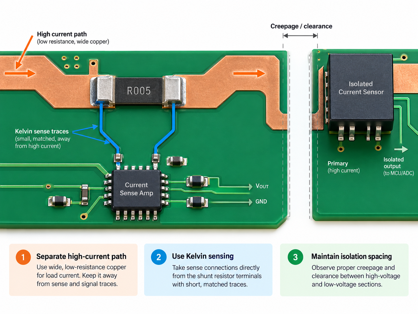
Step 2: Control soldering and rework. Qualify paste, flux, thermal profiles and manual processes as a combined residue and workmanship system.
Step 3: Clean where the risk assessment requires it. Select chemistry, time, temperature, agitation, rinse and drying controls that reach low-standoff areas without damaging materials.
Step 4: Validate cleanliness. Use methods appropriate to the failure risk. Bulk ionic testing, ion chromatography and surface insulation resistance answer different questions and should not be treated as interchangeable pass labels.
Step 5: Mask and coat consistently. Protect connectors, test points, thermal interfaces and other keep-out zones. Control material mixing, viscosity, application method, thickness and cure.
Step 6: Inspect the completed assembly. Check coverage, bubbles, pinholes, cracks, dewetting, contamination, staking, fasteners and masked areas with the specified lighting or fluorescence method.
Step 7: Run electrical tests. Perform the defined functional, insulation and safety tests after all protective materials have cured.
What Files Are Required for PCB Fabrication for Harsh Environments?
Put mandatory requirements, allowed substitutions and deliverable evidence in the controlled production package. If the stackup is in one email, the coating keep-outs in another and the test criteria in a meeting note, the supplier cannot quote or build against one reliable revision.
Insulation: minimum creepage, clearance, high-voltage keep-outs, slots and coating boundaries.
Assembly mechanics: component ratings, alternates policy, connector plating and support details.
Special processes: cleaning, bake, masking, coating, staking, potting, cure and rework instructions.
Inspection: test coupons, microsections, electrical test, AOI, X-ray and other required evidence.
Qualification: environmental test plan, specimen configuration and pre/post-test measurements.
Traceability: lot records, deviation approval, process-change notification and record-retention requirements.
What Qualification Evidence Should Procurement Request From PCB and EMS Suppliers?
Ask for evidence that identifies the design, lot or qualified process you are buying. Match each record to the purchase order, controlled drawing revision, material lot or assembly lot so the delivered evidence can be traced to the hardware.
Material evidence: laminate and prepreg identity, approved substitutions, date or lot traceability and relevant supplier datasheets.
Bare-board evidence: final stackup, electrical-test result, impedance data where required, microsection results and acceptance records for the specified interconnects.
Assembly evidence: approved BOM and alternates, soldering profiles where contractually required, inspection results, rework history and cleanliness validation.
Protection evidence: coating or potting material lot, application settings, cure record, measured thickness or coverage verification and defect disposition.
Qualification evidence: test plan, specimen identity, calibration status, raw or summarized measurements, photographs and pre/post-test functional results.
Change control: documented notification and approval before changing laminate, chemistry, coating, facility, critical process or component source where the contract requires it.
Which Tests Qualify PCB Fabrication for Harsh Environments?
A useful qualification test stresses the same mechanism that threatens the product in service. The IEC 60068 series provides widely used environmental methods, and IPC methods cover relevant board, coating and cleanliness properties. The mission profile and governing product standard still decide the method, severity, powered state and sequence.
Test family
Primary question
Evidence to retain
High and low temperature
Does the assembly function and remain within component, material and interface limits?
Board and component temperatures, operating state, functional data and visual inspection
Thermal cycling or thermal shock
Can interconnects, solder joints and material interfaces survive repeated expansion mismatch?
Profile, cycle count, continuity monitoring, resistance change, X-ray or microsection where justified
Damp heat or temperature-humidity-bias
Will moisture, contamination and electrical bias cause leakage, corrosion or migration?
Humidity and temperature record, bias conditions, insulation or SIR data and failure-site analysis
Vibration and mechanical shock
Do the board, fasteners, connectors and heavy components survive the system load?
Fixture and orientation, acceleration spectrum, resonance information, functional monitoring and post-test inspection
Salt mist or mixed-corrosion exposure
Are exposed metals, finishes, coating edges and enclosure interfaces resistant to the expected corrosive environment?
Solution or gas conditions, specimen orientation, exposure sequence, corrosion rating and electrical results
Electrical safety and function
Does the protected assembly maintain insulation, withstand voltage and required operation?
Test voltage or operating conditions, leakage or insulation values, functional limits and calibration records
Sequence can change the result. Vibration may open a coating crack that only becomes electrically significant during the following humidity exposure. On the other hand, piling tests together without a failure-mechanism rationale can leave you unable to identify the initiating cause. Keep an untested control sample when it will help separate normal build variation from environmental damage.
How Should Harsh-Environment PCB Failures Be Diagnosed?
Begin failure analysis with the symptom, exposure history and physical evidenceânot with the first damaged component. Replacing that component may restore operation while leaving the initiating cause, such as corrosion, cracked plating, contamination or mechanical strain, on the board.
Step 1: Preserve evidence. Record operating conditions, enclosure state, contamination, connector condition and failure timing before cleaning or disturbing the assembly.
Step 2: Localize the electrical symptom. Compare rails, insulation resistance, signal integrity, intermittent continuity and temperature behavior with a known-good unit.
Step 3: Inspect non-destructively. Use controlled visual inspection, microscopy, X-ray, ultraviolet coating inspection and thermal imaging as appropriate.
Step 4: Target destructive analysis. Cross-section suspect vias or solder joints, analyze residues or corrosion products, and examine interfaces only after the location has been narrowed.
Step 5: Reconstruct the mechanism. Decide whether the initiating condition was moisture, contamination, thermal fatigue, vibration, material incompatibility, coating defect, enclosure ingress or a combination.
Step 6: Verify corrective action. Update the design or process and repeat the stress that reproduced the failure, including post-test electrical and physical checks.
Useful clues include opens that appear only at certain temperatures, dendritic growth between biased conductors, corrosion products near residue, circumferential barrel cracks, solder fatigue beside heavy connectors and coating separation over a dirty or poorly cured surface. Each clue narrows the investigation; none should be called the root cause until inspection and analysis support it.
FAQs About PCB Fabrication for Harsh Environments
Q1: Can standard FR-4 be used in a harsh environment?
A1: Yes, in some applications. FR-4 is a family of materials, not one performance grade. Compare the selected grade’s thermal, expansion, moisture, electrical and CAF-related properties with the mission profile. Coating and enclosure protection may make it suitable for one installation, while another needs a different laminate or substrate.
Q2: Does a high Tg make a PCB suitable for continuous high-temperature operation?
A2: No. A high Tg does not by itself establish a PCB’s allowable continuous operating temperature. Review the laminate manufacturer’s long-term thermal data or applicable RTI, while treating Td and time-to-delamination results as short-duration thermal-robustness indicators rather than service-temperature ratings. Then check component and connector limits, plated-hole and solder-joint fatigue, coating limits, and measured board and component temperatures under power.
Q3: Can conformal coating make a PCB waterproof?
A3: No. Conformal coating is not a waterproof enclosure. Moisture can enter through coverage gaps, connectors, board edges, capillary paths or mechanical damage. Splash, immersion and pressure washing normally require equipment-level sealing and representative ingress testing.
Q4: Must a no-clean assembly be cleaned before coating?
A4: Decide from process validation, not from the âno-cleanâ label. Residue amount and chemistry, component standoff, humidity, electrical bias and coating adhesion all affect the result. Use a cleanliness method that can detect the failure risk you are trying to control.
Q5: Is potting always better than conformal coating for marine electronics?
A5: No. Potting trades serviceability and thermal freedom for a stronger local barrier. Marine reliability still depends on enclosure sealing, connectors, compatible metals, edge coverage and keeping saline moisture away from interfaces.
Q6: What is the main PCB risk in underground mining equipment?
A6: The combination of moisture and contamination is often the first concern. Conductive dust, corrosive gases, vibration and limited maintenance access can compound it. Document the actual atmosphere and safety requirements before choosing materials, spacing, enclosure and protection processes.
Q7: Are thermal shock and temperature cycling the same test?
A7: No. The transition rate and heat-transfer conditions are different. Select the method that reproduces the intended failure mechanism and meets the applicable standard; the two names are not interchangeable test specifications.
Q8: How is conformal coating thickness verified?
A8: Use a method matched to the coating and the location being controlled. Options include wet-film checks, cured witness coupons, mechanical or electronic gauges and microscopic cross-sections. One easy measurement on a flat area may say nothing about coverage around leads and board edges.
Q9: Does heavier copper solve every high-temperature PCB problem?
A9: No. Heavier copper solves only part of the thermal problem. Component losses, dielectric limits, via reliability, enclosure temperature, airflow and interface resistance remain in the heat path. Heavier copper also changes fabrication and soldering constraints.
Q10: How can procurement verify a supplier’s harsh-environment experience?
A10: Request evidence tied to the proposed construction. Useful records include material controls, final stackup, microsections, cleanliness and coating validation, environmental test documentation, traceability and change control. Each record should identify the applicable drawing, material lot or assembly lot.
Conclusion
Trace every important service stress to a drawing requirement, a production record and an acceptance test. If any link is missing from the harsh-environment PCB build package, the requirement is too vague for consistent production or a later failure investigation.
For a fabrication and assembly review, send the mission profile, stackup, Gerber or ODB++ data, BOM, assembly drawings and proposed qualification plan to sales@bestpcbs.com. The review is most useful when the operating environment and acceptance criteria arrive with the design files, not after the first prototype fails.
The semiconductor supply chain depends on far more than the chip itself. A semiconductor chip may be only a few millimeters across, but producing it depends on a surprisingly long chain of materials, chemicals, substrates, gases, passive components, and PCB materials. A shortage at almost any point in this chain can slow production even when wafer capacity itself is available.
That is why semiconductor supply-chain discussions should not focus only on silicon wafers. Materials such as photoresist, high-purity process gases, ABF substrates, copper foil, electronic-grade glass cloth, and passive components can become equally important bottlenecks.
The following 12 materials and components show how closely semiconductor fabrication, advanced packaging, PCB manufacturing, and electronics assembly are connected.
1. Indium Phosphide
Indium phosphide (InP) is a compound semiconductor material mainly used in high-frequency and optoelectronic devices.
It is commonly found in:
Optical communication systems
Photonic integrated circuits
Laser diodes
High-speed transistors
RF and microwave devices
Data-center optical modules
InP performs well in applications involving very high frequencies and light transmission.
Its supply chain is more specialized than conventional silicon. Crystal growth, wafer preparation, epitaxy, and device fabrication require dedicated processes, so production capacity cannot be expanded as easily as standard silicon manufacturing.
2. Photoresist
Photoresist is a photosensitive material used during semiconductor lithography. A thin layer is coated onto the wafer and exposed through a patterned mask. After development, the remaining resist defines where later processes such as etching, deposition, or implantation will take place.
As circuit geometries shrink, photoresist must provide tight control over:
Resolution
Film uniformity
Sensitivity
Purity
Defect density
Line-edge accuracy
Photoresist is also used in PCB fabrication to define copper circuitry. The basic concept is similar, although semiconductor lithography operates at a much finer scale and under much stricter contamination requirements.
3. Silicon Carbide
Silicon carbide (SiC) is a wide-bandgap semiconductor material widely used in high-power electronics.
It is particularly suitable for systems that operate at high voltage, high temperature, or high switching frequency.
Typical applications include:
EV traction inverters
On-board chargers
DC-DC converters
Fast chargers
Solar inverters
Industrial motor drives
Data-center power supplies
SiC devices can reduce switching losses and improve power density, but manufacturing the wafers is difficult.
Crystal growth, slicing, polishing, epitaxy, and device processing all require precise control, which is one reason SiC supply has attracted attention as electric vehicles and power electronics expand.
4. Copper Foil
Copper foil is one of the core conductive materials used in PCB manufacturing.
After lamination and patterning, it becomes the board’s:
Signal traces
Power planes
Ground planes
Pads
Thermal structures
Copper thickness matters for current capacity, while surface roughness becomes especially important in high-frequency and high-speed designs.
Heavy copper boards need thicker copper for power handling and heat distribution. High-speed boards may require lower-profile copper to reduce conductor loss.
Although copper foil sounds like a basic material, its thickness, roughness, adhesion, and mechanical properties can directly affect PCB performance.
5. Tantalum Capacitors
Tantalum capacitors are electronic components rather than semiconductor raw materials, but they still matter in the wider electronics supply chain.
They are used where designers need relatively high capacitance in a compact package, including:
Power filtering
Industrial electronics
Telecom equipment
Aerospace systems
Medical devices
Automotive electronics
For PCBA production, a small passive component can become a bottleneck.
If a qualified tantalum capacitor is unavailable, replacing it may require checking voltage rating, capacitance, ESR, package size, reliability requirements, and approved alternatives before assembly can continue.
6. ABF Substrates
ABF substrates are widely used in advanced semiconductor packaging.
ABF stands for Ajinomoto Build-up Film, an insulating material used in high-density package substrates.
These substrates create the electrical connection between fine-pitch semiconductor packages and the larger interconnect structures on the PCB.
They are commonly associated with:
CPUs
GPUs
AI accelerators
Networking processors
High-performance computing devices
As package I/O density increases, substrate routing becomes finer and more complex.
Wafer capacity alone therefore does not determine how many finished chips can enter the market. Advanced packaging and substrate availability can become separate constraints.
7. High-Purity Nitrogen
Nitrogen is common in industry, but semiconductor manufacturing requires very high purity and controlled delivery.
It is used for:
Equipment purging
Oxygen displacement
Wafer handling
Chamber protection
Drying
Controlled process atmospheres
Semiconductor processes are highly sensitive to contamination, so trace moisture, particles, oxygen, or chemical impurities can affect process stability and yield.
High-purity nitrogen also has a place in electronics assembly. Nitrogen-assisted reflow and soldering processes may be used when oxidation control is important.
They are used for decoupling, filtering, bypassing, and power stabilization.
Supply becomes more sensitive when a design combines demanding requirements such as:
Very small package sizes
High capacitance
Higher voltage
Automotive qualification
Tight tolerance
Specific temperature characteristics
An MLCC with the same nominal capacitance is not always a direct substitute.
Engineers may also need to review dielectric type, DC bias behavior, package size, voltage rating, temperature coefficient, and qualification requirements before approving an alternative.
9. Molybdenum Sputtering Targets
Molybdenum sputtering targets are used in physical vapor deposition processes.
During sputtering, atoms are released from the target and deposited as a thin film onto another surface.
For semiconductor and electronic applications, target quality depends on more than the molybdenum itself.
Manufacturers need to control:
Material purity
Density
Grain structure
Contamination
Dimensional consistency
Bonding quality
Minor impurities that are acceptable in ordinary industrial metal may create problems during high-precision thin-film processing.
Semiconductor-grade sputtering targets therefore belong to a highly controlled specialty-material supply chain.
10. Electronic-Grade Sulfuric Acid
Sulfuric acid is widely used in industry, but semiconductor production requires ultra-high-purity electronic-grade material.
It is used in wafer cleaning and other chemical processes where trace contamination must remain tightly controlled.
Key concerns include:
Metallic impurities
Particles
Organic contaminants
Ionic contamination
Producing industrial sulfuric acid and producing semiconductor-grade sulfuric acid are very different manufacturing tasks.
The purification system, packaging, transportation, handling, and quality controls all need to meet semiconductor processing requirements.
11. High-End PCB Substrates
After a semiconductor is packaged, it still needs a circuit board capable of supporting its electrical and thermal requirements.
Standard FR-4 is suitable for many products, but high-speed, RF, automotive, computing, and industrial designs may need laminates with tighter control over:
Dielectric constant
Dissipation factor
Tg
Thermal expansion
Moisture absorption
Dimensional stability
Copper adhesion
For these boards, material selection is part of the engineering process.
A laminate with similar mechanical specifications may behave very differently at multi-gigabit data rates or during repeated thermal cycling.
12. Electronic-Grade Glass Fiber Cloth
Electronic-grade glass fiber cloth is a reinforcement material used in many PCB laminates.
The cloth is impregnated with resin to form prepreg, which is then laminated with copper foil and core materials to build the PCB structure.
Important properties include:
Cloth thickness
Weave style
Yarn size
Resin impregnation
Dimensional stability
Surface uniformity
Glass weave can also affect high-speed signal behavior.
At very high data rates, traces passing over different glass and resin regions can experience small variations in effective dielectric properties. Material selection, routing strategy, and spread-glass constructions can help control this effect.
How Do Semiconductor Material Constraints Affect PCB and PCBA Production?
Before a finished electronic product can be built, the project depends on PCB materials, passive components, connectors, assembly materials, and manufacturing capacity.
Several materials discussed above connect directly with PCB and PCBA production:
Copper foil affects conductor construction and electrical performance.
Glass cloth and laminate systems influence PCB mechanical and dielectric properties.
MLCCs and tantalum capacitors affect BOM availability and assembly scheduling.
High-performance substrates become more important as signal speed and power density increase.
Sourcing and engineering therefore need to work together in complex PCB and PCBA projects, particularly when materials or components have limited qualified alternatives.
Which Materials Matter Most in PCB Manufacturing?
For PCB fabrication, the most relevant items from the list are copper foil, laminate materials, and electronic glass cloth.
Together, these materials define much of the board’s electrical, mechanical, and thermal behavior.
Engineers may need to evaluate:
Dk and Df
Tg and thermal stability
CTE
Copper thickness
Copper roughness
Moisture absorption
CAF resistance
Dimensional stability
These parameters become more important in HDI, RF, high-speed, high-current, heavy copper, automotive, and other demanding boards.
For example, low-loss laminate may matter far more than standard FR-4 in high-speed interfaces, while copper thickness and thermal design become central in high-current power boards.
How Do Component Shortages Affect PCBA Assembly?
A bare PCB can be fully manufactured and still sit idle if critical BOM components are missing.
Component availability should therefore be reviewed early, especially for parts that are difficult to substitute.
Important checks include:
Manufacturer part number
Package and footprint
Lifecycle status
Lead time
Approved alternatives
Electrical specifications
Reliability grade
Supply continuity
Passive components deserve attention as well.
An MLCC or tantalum capacitor may look simple, but replacement can require engineering approval when voltage, dielectric behavior, package size, temperature performance, or qualification requirements differ.
How Can PCB and PCBA Buyers Reduce Supply-Chain Risk?
The practical approach is to identify critical materials and components before production starts.
For PCB projects, buyers should clearly define material, stack-up, copper thickness, impedance, surface finish, and any special thermal or reliability requirements.
For PCBA projects, the BOM should include accurate manufacturer part numbers and approved alternatives where possible.
Several steps can improve sourcing flexibility:
Perform DFM and BOM review early.
Approve equivalent PCB materials where technically acceptable.
Identify long-lead-time and single-source components.
Review alternative parts with engineering, not purchasing alone.
Separate ordinary BOM items from supply-critical parts.
Confirm material availability before mass production.
The goal is to avoid discovering a sourcing problem after production has already started.
How EBest Circuit Supports PCB and PCBA Manufacturing
At EBest Circuit, we support PCB and PCBA projects from engineering review and PCB fabrication through component sourcing, assembly, inspection, and testing.
Our PCB capabilities include:
Rigid PCB
Flex and rigid-flex PCB
HDI PCB
Heavy copper PCB
RF and microwave PCB
High-speed PCB
High-current PCB
For PCBA projects, EBest Circuit can also coordinate:
Component sourcing
SMT assembly
Through-hole assembly
Inspection
Testing
Before production, our engineering team can review key project information such as:
Gerber files
BOM
Pick-and-place data
PCB stack-up
Material requirements
Controlled impedance
Copper thickness
Assembly notes
Testing requirements
This allows PCB fabrication, component sourcing, and PCBA assembly requirements to be reviewed within the same project workflow.
Conclusion
These 12 materials and components show that semiconductor supply is closely tied to PCB and electronics manufacturing.
Some are used inside semiconductor fabrication. Others become important during advanced packaging, PCB production, component sourcing, and PCBA assembly.
For PCB and PCBA buyers, the practical issue is broader than chip availability. PCB materials, BOM components, fabrication requirements, assembly, and sourcing all need to align before a product can move smoothly into production.
If you have a PCB or PCBA project, send EBest Circuit your Gerber files, BOM, stack-up, and technical requirements for engineering review and quotation.
Artificial intelligence in PCB assembly optimization is becoming more practical as SMT lines generate increasing amounts of production and inspection data. SPI, placement machines, reflow ovens, AOI, X-ray inspection, testing, and traceability systems all provide information that can be used to identify process patterns. AI helps connect these data points, allowing engineers to detect abnormalities earlier and investigate why defects occur rather than only where they are found.
For PCB assembly buyers, the real value is better process control, inspection, and yieldânot AI for its own sake. EBest Circuit supports PCB fabrication, PCBA assembly, and box-build projects from prototypes to volume production. If your project has demanding assembly, inspection, testing, or traceability requirements, send your Gerber files, BOM, and assembly requirements to sales@bestpcbs.com for an engineering review.
What Is AI in PCB Assembly?
AI in PCB assembly refers to the use of machine learning, computer vision, pattern recognition, and data analytics to support manufacturing decisions.
Traditional PCB assembly relies on machine programs, process limits, SPC, inspection rules, and engineering experience. AI adds another layer by analyzing larger volumes of production data and identifying relationships between different process variables.
For example, an AOI defect may be linked to solder paste volume, placement offset, component geometry, or reflow conditions. Instead of examining each stage separately, AI can help correlate these records.
AI is therefore most useful when it works alongside established process controls and manufacturing engineering rather than replacing them.
How Is AI Used in PCB Assembly?
AI can be applied across several stages of PCB assembly because each stage produces different types of manufacturing data.
Typical sources include:
SPI: solder paste height, area, volume, and offset;
Placement: coordinates, corrections, feeder and nozzle data;
Reflow: temperature profiles, zone settings, and conveyor speed;
Inspection: AOI images, X-ray images, and defect records;
Testing: ICT, functional test, and failure results;
Traceability: PCB serial numbers, material lots, machines, and production history.
The key advantage comes from connecting these records.
If AOI repeatedly finds insufficient solder on the same package, engineers can compare those failures with earlier SPI, placement, and reflow data. This shifts the investigation from where a defect was detected toward which upstream condition may have contributed to it.
That cross-process visibility is one of the main ways AI can support PCB assembly optimization.
How Does AI Optimize the SMT Assembly Process?
AI can help engineers analyze relationships between solder paste printing, placement, reflow, and downstream inspection results.
Solder Paste Printing
SPI data can reveal changes in paste volume, height, area, or offset. When these measurements are compared with later defects, engineers can identify patterns that deserve attention.
Component Placement
Placement data can reveal repeated corrections associated with a particular component, feeder, nozzle, or board location. Instead of treating each adjustment as an isolated event, historical data can show whether the pattern is becoming systematic.
Reflow Soldering
AI can compare production results with variables such as zone temperature, conveyor speed, package size, and board characteristics. This can help engineers narrow down process combinations associated with recurring soldering problems.
The objective is not to replace thermal profiling or process engineering. It is to use historical production data more effectively so engineers can investigate potential causes and make process adjustments with better evidence.
How Does AI Improve PCB Assembly Inspection?
Inspection is one of the most practical areas for AI in PCB assembly because modern inspection equipment already generates large amounts of image and measurement data.
AOI
AOI may inspect conditions such as:
missing or misplaced components;
polarity errors;
solder bridges;
insufficient solder;
lifted leads;
abnormal solder-joint appearance.
Machine-learning models can help distinguish actual defects from acceptable process variation. This is particularly useful when conventional inspection rules generate excessive false calls.
X-Ray Inspection
AI can also support X-ray analysis for hidden solder joints under BGA, QFN, and other bottom-terminated packages. Typical inspection targets include voiding, bridging, insufficient solder, alignment issues, and hidden joint abnormalities.
The practical benefit is not simply detecting more features. Better classification can reduce unnecessary review while making inspection results more useful for upstream process correction.
How Does AI Detect PCB Assembly Defects?
AI-based defect detection commonly uses computer vision or measurement data to recognize patterns associated with known assembly defects.
Depending on the inspection method, these may include:
missing components;
component shift;
reversed polarity;
tombstoning;
solder bridges;
insufficient solder;
lifted leads;
hidden solder-joint abnormalities.
A trained model can compare new inspection data with previously classified examples and estimate whether a condition represents normal variation or a genuine defect.
AI can also help group repeated failures. If the same defect appears on one reference designator, package type, component lot, or production line, the pattern becomes easier to identify.
However, reliable detection still depends on representative training data and consistent defect classification. AI can improve the speed of analysis, but inspection criteria and engineering validation remain essential.
How Does AI Improve PCB Assembly Yield?
AI can support PCB assembly yield improvement by connecting defect results with the process conditions that occurred earlier in production.
Instead of looking only at the final yield percentage, engineers can compare failures with:
SPI measurements;
placement corrections;
reflow conditions;
AOI or X-ray results;
component lots;
repair records;
electrical test failures.
This can make recurring failure patterns easier to identify.
First-Pass Yield
First-pass yield is particularly useful because repeated inspection, repair, and retesting add time and handling to the assembly process. AI-based analysis can help engineers focus on process variables that show a strong relationship with recurring defects.
Root-Cause Analysis
Connected production data can also reduce the time needed to trace a defect back through earlier processes.
For example:
AOI detects a solder defect â SPI history shows abnormal paste variation â engineers inspect stencil or printing conditions.
The practical goal is straightforward: identify problems earlier and shorten the path from defect detection to corrective action.
What Data Does AI Need for PCB Assembly Optimization?
Useful AI analysis depends more on data quality and traceability than simply collecting a large quantity of data.
Common inputs include:
SPI measurements;
placement and correction records;
reflow parameters;
AOI and X-ray results;
defect classifications;
rework records;
ICT and functional test results;
PCB serial numbers;
component lot information;
machine and production timestamps.
Traceability is especially important. If a failed board cannot be connected to its earlier manufacturing history, root-cause analysis becomes much harder.
Consistent labeling also matters. Similar defects should not be recorded under several unrelated names if the data will later be used for model training or statistical analysis.
For many manufacturers, improving data structure is therefore an important first step before introducing more advanced AI tools. Good manufacturing data gives both AI systems and engineers a stronger basis for decision-making.
What Are the Challenges of Using AI in PCB Assembly?
One challenge is high-mix production. An EMS factory may assemble many PCB designs with different packages, materials, volumes, and inspection requirements. A model that performs well on one product may require adjustment for another.
Other practical issues include:
inconsistent data formats between equipment;
limited historical data for prototypes or low-volume builds;
false positives and missed defects;
process changes after material or equipment adjustments;
inconsistent defect labeling.
AI also identifies correlations, which are not always the same as root causes. A change in defect rate may coincide with a reflow adjustment, for example, while the actual cause is related to solder paste, PCB design, component condition, or another variable.
For this reason, AI works best as an engineering support tool.
The most reliable approach combines production data, AI analysis, established process controls, and manufacturing engineering judgment.
FAQs About Artificial Intelligence in PCB Assembly Optimization
Can AI completely automate PCB assembly optimization?
Not in most production environments. AI can assist with inspection, process analysis, prediction, and troubleshooting, while engineers still validate process changes and product-specific requirements.
What PCB assembly data can AI analyze?
AI can analyze SPI measurements, placement data, reflow records, AOI and X-ray images, defect history, rework records, traceability information, and electrical test results.
Can AI reduce PCB assembly defects?
AI can identify patterns associated with recurring defects and help engineers detect abnormal process trends earlier. Actual defect reduction comes from applying appropriate corrective actions based on those findings.
Is AI suitable for low-volume PCB assembly?
Yes, although the approach may differ from mass production. Low-volume projects may have less product-specific historical data, so generalized inspection models, cross-product data, and engineering rules become more important.
How is AI different from traditional PCB assembly process control?
Traditional process control relies on defined limits, machine settings, SPC, inspection criteria, and engineering experience. AI adds pattern recognition and predictive analysis across larger datasets. In practice, the two approaches complement each other.
If you are developing a PCB or PCBA project and need support with assembly process control, inspection, testing, or traceability, EBest Circuit can review your manufacturing files before production. Send your Gerber files, BOM, assembly drawings, test requirements, and expected quantity to sales@bestpcbs.com so our team can evaluate the project and prepare an appropriate manufacturing and quotation plan.
what does e.m.s stand for depends on the industry in which the abbreviation appears. In electronics manufacturing, EMS means Electronics Manufacturing Services: outsourced services that can cover product introduction, supply-chain execution, PCB fabrication, PCB assembly, testing, box build and lifecycle support. The same letters can mean something entirely different in medicine, environmental compliance or energy management, so the surrounding technical context matters.
What Does E.M.S Stand For?
EMS is an acronym rather than a single universal term. A document mentioning an ambulance service, an ISO 14001 program, a factory energy dashboard or a circuit-board production line may use the same three letters for unrelated concepts.
Context
Common EMS meaning
Clue in the document
Electronics
Electronics Manufacturing Services
BOM, SMT, PCBA, testing, box build
Medical response
Emergency Medical Services
Ambulance, paramedic, emergency care
Environmental management
Environmental Management System
ISO 14001, aspects, compliance, audit
Energy operations
Energy Management System
Metering, load control, energy efficiency
Physical therapy or fitness
Electrical Muscle Stimulation
Electrodes, pulses, muscle contraction
In a manufacturing specification, supplier list or electronics program plan, EMS normally refers to the first meaning in the table.
Why Does the Meaning of EMS Depend on Context?
Acronyms compress language, but they also remove context. The reliable way to interpret EMS is to identify the objects and actions around it. Terms such as schematic, Gerber, AVL, solder paste, AOI and functional test point to electronics manufacturing. Terms such as emergency care, environmental audit or energy monitoring point elsewhere.
Punctuation does not change the expansion. E.M.S., E.M.S and EMS are typographic variants. Electronics companies generally use the unpunctuated form, while a search written with periods can still be seeking the manufacturing definition.
What Does EMS Stand For in Electronics Manufacturing?
In electronics, EMS stands for Electronics Manufacturing Services. An EMS provider manufactures, assembles, tests and supports electronic products for another company under an agreed technical and commercial scope. The customer may be an original equipment manufacturer, an industrial product developer, a medical-device company or another organization that owns the product requirements.
The term describes a service model, not a particular factory process. One program may cover only PCB assembly, while another includes design-for-manufacturing review, component sourcing, FR4 PCB fabrication, programming, functional testing, enclosure integration and shipment of finished units. Scope must therefore be defined by controlled documents rather than inferred from the label EMS.
Is It Electronic or Electronics Manufacturing Services?
Electronics Manufacturing Services is the established industry expansion of EMS. âElectronic manufacturing servicesâ is also understandable and appears in general writing, but it describes the activity more loosely. The plural noun âelectronicsâ refers to the industry and is the clearer form for contracts, capability statements and supplier categories.
Related phrases include electronics contract manufacturing, electronic contract manufacturing and contract electronics manufacturing. They overlap substantially, although some companies use âcontract manufacturingâ for a narrower build-to-print scope and reserve EMS for broader engineering, supply-chain and lifecycle support.
What Does an EMS Provider Actually Control?
An EMS provider controls manufacturing execution within the boundaries approved for the program. That normally means converting released product data into a repeatable production route, maintaining process instructions, controlling materials, recording inspection results and managing nonconforming output.
Process planning: panel handling, stencil strategy, placement sequence, reflow profile, inspection points and test flow.
Authorized sourcing: purchasing against the approved BOM and AVL, with substitutions controlled by the agreed change process.
Production records: material lots, work orders, inspection history, test results and disposition records at the traceability level specified for the product.
Manufacturing feedback: DFM, DFA and DFT findings that identify yield, assembly or testability risks before volume production.
Control is not the same as ownership. The provider can recommend a pad change or alternate component, but it should not silently change released product data.
What Does the OEM Retain Control Of?
The OEM usually retains ownership of the product definition: performance requirements, system architecture, intellectual property, approved schematics, released PCB data, firmware, branding and market obligations. It also defines which deviations require formal approval and who can release a new revision.
A practical responsibility matrix should identify the owner for each deliverable. For example, the OEM may own the master BOM and acceptance criteria, while the EMS provider owns machine programs and work instructions derived from those inputs. Regulatory files, cybersecurity decisions and product-level validation remain with the legally responsible organization unless a contract explicitly assigns supporting work.
How Are EMS, OEM, ODM and ECM Different?
The useful distinction is who owns the product design and how broad the contracted work is. Company labels vary, so the signed scope and controlled deliverables are more reliable than the acronym alone.
Model
Typical design ownership
Typical manufacturing role
OEM
Owns the branded product definition and market requirements
May manufacture internally or outsource part or all of production
EMS
Usually builds from customer-controlled product data
Can provide NPI, sourcing, fabrication, assembly, test, box build and lifecycle support
ODM
Owns or licenses a product platform that a customer can customize and brand
Designs and manufactures the resulting product
ECM/CM
Usually customer-owned design
Often used for build-to-print contract manufacturing; usage overlaps with EMS
A bare PCB is the manufactured interconnect structure; a PCBA is that board populated with electronic components. EMS can connect those stages, but they remain separate deliverables with different source files and inspection criteria.
PCB fabrication uses Gerber or ODB++ data, drill files, a stack-up, material requirements, controlled impedance information and a fabrication drawing. PCB assembly services add the BOM, centroid data, assembly drawings, polarity information, approved alternates, programming files and test requirements. A complete EMS program may then integrate the PCBA with cables, displays, thermal hardware and an enclosure.
This separation matters during revision control. A schematic change can affect the BOM, PCB layout, firmware and test procedure at the same time; every affected artifact must move to a compatible revision before production resumes.
Which Manufacturing Services Sit Inside an EMS Program?
An EMS program can contain several linked manufacturing modules. The required combination depends on the released scope, but each module should have its own inputs, acceptance criteria and records.
NPI planning, manufacturability review and process development
Component sourcing and incoming-material control
Bare-board fabrication and electrical testing
SMT, through-hole or mixed-technology assembly
Programming, inspection, electrical test and functional verification
Box build, cable integration, labeling and configured packaging
Repair, rework, revision transition and end-of-life support when contracted
An SMT stencil, for example, is a process tool rather than part of the finished product, yet its aperture design and revision directly affect solder-paste deposition and assembly yield.
How Does an EMS Project Move From NPI to Production?
NPI converts design data into a controlled manufacturing process. The first step is a data-set review that checks file completeness and revision consistency. DFM, DFA and DFT findings are then closed or formally accepted before machine programming and tooling are frozen.
Release review: verify BOM, AVL, fabrication data, drawings, firmware and test specifications.
Process preparation: define panel handling, paste printing, placement, reflow, manual assembly, inspection and test routes.
Pilot build: assemble a limited lot to validate tooling, component fit, process windows and test coverage.
First-article approval: compare the built unit with dimensional, electrical, workmanship and functional criteria.
Production release: freeze approved programs and instructions, then monitor yield and defects against defined limits.
A pilot build is valuable only when its findings change the controlled process. A defect log without assigned disposition, updated instructions and verified corrective action does not complete NPI.
How Are Engineering Changes Controlled in EMS?
Engineering change control prevents a valid new document from being combined with an obsolete companion file. Every production release should identify the compatible revisions of the BOM, PCB data, assembly drawing, firmware and test procedure.
A controlled change normally records the reason, affected part numbers, inventory disposition, effective work order, required validation and approval authority. Temporary deviations should have an expiration or quantity limit. When an alternate component changes package geometry, electrical behavior or firmware interaction, a purchasing approval alone is insufficient; the affected manufacturing and test documents must also be reviewed.
How Is Quality Verified in Electronics Manufacturing Services?
Quality verification should match the failure modes of the assembly. Solder-paste inspection detects deposit volume or alignment problems before components are placed. AOI checks visible component and solder-joint conditions. X-ray is used where joints are hidden, such as BGA and bottom-terminated packages. Functional testing confirms behavior that optical inspection cannot prove.
At EBest Circuit (Best Technology), relevant assembly programs can combine SMT, THT or mixed assembly with 3D SPI, AOI, X-ray and functional testing. The inspection route should be selected according to package type, defect visibility and required test coverage; adding every test indiscriminately increases handling without necessarily improving detection.
Which Industries Use EMS Providers?
EMS providers support products in industrial control, communications, automotive electronics, medical equipment, instrumentation, consumer electronics, energy systems and aerospace-related applications. The manufacturing steps may look similar, but documentation, traceability, environmental testing, change approval and product validation differ substantially by industry and program.
For example, an industrial controller may prioritize long component availability and field-service records, while a compact communication product may prioritize fine-pitch assembly, RF performance and thermal control. âIndustry experienceâ is meaningful only when it maps to the applicable materials, processes, inspection coverage and documentation.
FAQ About What E.M.S Stands For
Is PCB Assembly the Same as EMS?
No. PCB assembly is one manufacturing service. EMS is a broader operating model that may include NPI, sourcing, PCB fabrication, PCBA, programming, testing, box build, logistics and lifecycle support.
Can an EMS Provider Own the Product Design?
An EMS provider can perform design services, but design ownership depends on the contract. In a conventional build-to-print program, the customer owns the released product data. An ODM arrangement more commonly uses a supplier-owned platform or design.
Is EMS Only for High-Volume Production?
No. EMS programs can support prototypes, high-mix low-volume production and sustained volume manufacturing. The appropriate equipment, tooling, material strategy and process controls differ across those production profiles.
What Does EMS Mean on a Supplier List?
On an electronics supplier list, EMS usually identifies a company that provides outsourced electronics manufacturing. The approved scope may still be restricted to particular sites, processes, product families or certifications.
Can EMS Include Box Build and Repair?
Yes. Box build, cable integration, programming, final test, repair and return analysis can be included when their technical inputs, acceptance criteria, records and ownership boundaries are defined.
Conclusion
In an electronics context, what does e.m.s stand for has a direct answer: Electronics Manufacturing Services. The more important engineering question is what the contracted scope includes and where control passes between the product owner and the manufacturing provider. Clear release data, responsibility boundaries, revision control and test coverage turn the acronym into a workable production system.
For PCB fabrication, PCBA and electronics manufacturing support, contact EBest Circuit (Best Technology) at sales@bestpcbs.com.
An automotive IR illuminator aluminum PCB carries current to infrared emitters, provides a stable mounting platform and transfers heat away from the LED array in driver monitoring and other in-cabin sensing systems. The PCB design has to work with the IR emitter package, current profile, camera field of view, beam pattern and module geometry.
Are you worried about these automotive IR illumination problems?
The IR LED array runs too hot during pulsed or continuous operation.
The camera sees uneven IR illumination, with bright and weak areas across the field of view.
The prototype works, but LED position, PCB construction or assembly quality becomes difficult to keep consistent in production.
As a professional one-stop PCB and PCBA service provider, EBest Circuit supports automotive IR illuminator aluminum PCB fabrication, component sourcing, PCB assembly, prototyping and mass production. Our solutions include:
Control Current and Heat Around the Emitters Match copper geometry, thermal dielectric and metal-core construction to the actual LED current and emitter layout.
Maintain Optical and Mechanical Alignment Control LED position, orientation, PCB dimensions and mounting features so the illuminator fits the camera module as designed.
Carry the Approved Build Into Production Keep the validated PCB construction and assembly requirements consistent when moving from prototypes to volume manufacturing.
For an automotive camera illumination aluminum PCB or in-cabin sensing IR aluminum PCB, send your Gerber files, IR LED datasheet and project requirements to sales@bestpcbs.com for a quotation.
What Is an Automotive IR Illuminator Aluminum PCB and Where Is It Used in In-Cabin Sensing?
An automotive IR illuminator aluminum PCB is a metal-based PCB used to mount and power infrared LEDs in automotive camera and in-cabin sensing modules. Its main functions are to carry LED current, hold the emitters in the required positions and transfer heat away from the IR LED array.
The board is part of the sensing module rather than a stand-alone lighting circuit. IR LED position, beam direction, camera location and housing geometry all affect how the illuminator performs after installation.
Depending on the optical design, the module may use 850 nm or 940 nm IR emitters.
Typical applications include:
Driver Monitoring Systems (DMS): Supports imaging of the driver’s face, eyes and head position.
Occupant Monitoring Systems (OMS): Provides IR illumination across passenger and seating areas.
Child Presence Detection: Supports camera-based sensing in low visible-light conditions.
Interior and Gesture Monitoring: Used in overhead consoles, displays and interior camera modules.
Eye-Tracking Systems: Provides controlled illumination around the driver’s eyes and facial area.
How Should an In-Cabin Sensing IR Aluminum PCB Handle LED Current and Heat?
An in-cabin sensing IR aluminum PCB needs to be designed around the actual LED current waveform, particularly when the emitters operate in pulsed or strobed modes.
Average current alone does not describe the load on the PCB. During a high-current pulse, the traces, pads, connectors and solder joints may carry a much higher instantaneous current.
Size Current Paths for Peak Current Use the actual pulse current when setting trace width and copper area. Narrow conductors increase resistance, voltage drop and localized heating.
Keep High-Current Paths Short Reduce unnecessary distance between the IR LED driver and emitter array. Shorter paths lower resistive loss and make current delivery easier to control.
Provide Enough Copper Around the Emitters Adequate copper supports current carrying and helps spread heat away from concentrated emitter areas.
Avoid Excessive Emitter Clustering Several high-current IR LEDs placed in a small area can create a localized thermal load. Their spacing needs to work for both optical coverage and heat distribution.
Include Driver Losses When the Driver Shares the PCB If the driver is mounted on the same automotive IR LED PCB, its losses become part of the total thermal load.
Define the Pulse Profile Provide peak current, pulse width and duty cycle during PCB review. These values describe the operating condition more accurately than a single nominal wattage.
How Should Automotive IR LED PCB Layout Support Camera Alignment and Uniform Illumination?
An automotive IR LED PCB layout needs to match the camera field of view and the required illuminated area. LED position, spacing, orientation and beam direction can all affect the image captured by the camera.
Match the IR Beam to the Camera Field of View A narrow beam may leave weak areas near the edges of the image. A beam that is too wide sends part of the IR output outside the useful sensing region.
Control IR LED Orientation Directional or asymmetric emitters need the correct rotation on the PCB. A component can be electrically correct and still illuminate the wrong area.
Distribute Emitters Across the Required Region Poor spacing can create excessive intensity in one area while leaving other parts of the camera image under-illuminated.
Use Stable Mechanical References Mounting holes, board edges and locating features need to match the camera or illuminator housing so the same optical alignment can be reproduced during assembly.
Keep the Optical Path Clear Screws, connectors, shields and tall components should not interfere with the IR beam.
Include Secondary Optics in the Mechanical Layout When the module uses lenses, light guides, diffusers or optical windows, their position and tolerances need to be coordinated with the PCB.
How Should Temperature, Vibration and Long Operating Cycles Affect Automotive IR PCB Design?
Automotive IR modules can experience repeated temperature changes, vibration and high-current emitter pulsing. These conditions affect solder joints, mounting features and the long-term stability of the PCB assembly.
Operating Temperature PCB materials, solder mask, surface finish and assembly materials need to suit the intended module environment.
Thermal Cycling Repeated heating and cooling places mechanical stress on solder joints and interfaces around high-current emitters.
PCB Mechanical Support Large connectors and unsupported board sections should not transfer unnecessary mechanical load to the IR LED solder joints.
Mounting-Hole Accuracy The PCB should fit the housing without being forced or bent during installation. Poor hole positioning can introduce mechanical stress into the finished module.
Component Retention Larger components and connectors may require additional mechanical support where vibration is expected.
Repeated Pulsed Operation High-current strobing creates recurring electrical and thermal loading. The current path and solder joints need to remain stable under the intended operating profile.
What Steps Are Used to Manufacture and Assemble an Automotive IR Illuminator Aluminum PCB?
An automotive IR illuminator aluminum PCB requires controlled fabrication and assembly so the emitter positions, current paths and approved metal-core construction remain consistent.
Step 1: Review the Design and IR LED Requirements
Check the IR LED part number, wavelength, footprint, polarity, orientation, peak current, copper weight, PCB thickness, thermal dielectric, mounting features and surface finish before production starts.
Step 2: Prepare the Metal-Core Laminate
Use the approved copper, dielectric and aluminum construction. A material change can affect thermal performance, finished thickness and mechanical fit.
Step 3: Form the Copper Circuit
Image and etch the IR LED pads, high-current paths and supporting circuitry. Trace width and spacing need to remain compatible with the selected copper weight.
Step 4: Drill and Profile the PCB
Produce mounting holes, slots and the finished board outline from the mechanical drawing. These features may directly control the position of the illuminator inside the camera housing.
Step 5: Apply Solder Mask and Surface Finish
Keep IR LED pads and other solderable areas correctly exposed. The selected surface finish needs to suit the component package and assembly process.
Step 6: Print Solder Paste
Match stencil openings and solder-paste volume to the IR LED package. Poor paste control can lead to uneven package seating after reflow.
Step 7: Place the IR LEDs
Control X/Y location and component rotation. Placement accuracy is especially important for directional or asymmetric emitters.
Step 8: Complete Reflow Soldering
Use a reflow profile suitable for the selected components. After soldering, check for poor wetting, package tilt, insufficient solder and other visible defects.
Step 9: Verify the Finished Assembly
Check IR LED polarity, electrical operation, current behavior and mechanical fit before the assembly moves to the next production stage.
What Steps Are Used to Inspect and Test Automotive IR Illuminator PCBs?
Inspection should concentrate on the characteristics that can affect current delivery, IR LED alignment, thermal transfer and final module operation.
Step 1: Verify PCB Construction
Check the aluminum base, thermal dielectric, copper thickness and finished PCB thickness against the approved build.
Step 2: Check Critical Dimensions
Inspect the board outline, mounting holes, slots and locating features used to position the illuminator inside the module.
Step 3: Inspect Circuit and Surface Quality
Use visual inspection and AOI where applicable to identify opens, shorts, damaged pads, contamination and solder-mask defects.
Step 4: Perform Electrical and Insulation Testing
Verify circuit continuity and electrical isolation between the conductive circuit and metal base.
Step 5: Verify IR LED Placement
Check the emitter part number, polarity, X/Y position and rotation against the approved assembly data.
Step 6: Inspect Solder Joints
Review solder wetting and package seating. A tilted IR emitter can affect both heat transfer and beam direction.
Step 7: Perform Functional Current Testing
Operate the assembly under the defined electrical conditions and check LED switching, current delivery and supporting circuit operation.
Step 8: Check Thermal Performance
For higher-current arrays, test the PCB under representative operating conditions. Pulsed designs need an appropriate peak current and duty cycle during validation.
Step 9: Verify Optical Output When Required
When the project includes optical acceptance criteria, test the illuminator using the specified camera, IR sensor or optical fixture rather than relying on visual inspection.
What Automotive IR Aluminum PCB Manufacturing Capabilities Can We Provide?
The table below summarizes our main MCPCB manufacturing capabilities for automotive IR illuminator PCB projects.
Item
Capabilities
Maximum Layer Count
Up to 10 layers
PCB Thickness
0.3â4.0 mm
Maximum Board Size
Up to 610 Ă 1220 mm (24 Ă 48 in.)
Copper Weight
0.5â10 oz
Minimum Trace / Space
0.15 / 0.15 mm (6 / 6 mil)
Minimum Hole Diameter
0.30 mm (12 mil)
Minimum Punch Hole Diameter
3.0 mm (0.12 in.)
Minimum Hole Spacing
0.40 mm (16 mil)
Maximum Aspect Ratio
12:1
Minimum Solder Pad Diameter
0.40 mm (16 mil)
Thermal Conductivity
0.8â1.5 W/m·K standard; 2.0â6.0 W/m·K high thermal conductivity
Warp and Twist
< 0.75%
Flammability
UL 94V-0
Thermal Stress
6 à 10 sec at 288°C
Surface Finish
ENIG, Flash Gold, Hard Gold, Selective Gold Plating, HASL, Lead-Free HASL, OSP, Immersion Silver, Immersion Tin
Case Study: Automotive IR Illuminator Aluminum PCB From Prototype to Production
Project Background
An in-cabin camera module required a compact automotive IR illuminator aluminum PCB for a high-current IR emitter array. The PCB had to fit the camera-module housing while holding the emitters in the positions defined by the optical design.
Project Requirements
The PCB needed to:
Carry the specified pulsed LED current
Keep IR emitter position and polarity consistent
Transfer heat into the metal substrate
Match the camera-module mounting geometry
Fit within the available module space
Support both prototype validation and repeat production
Our Solution
EBest Circuit reviewed the IR LED datasheet, PCB layout and mechanical drawing before prototype fabrication.
The project focused on:
Matching IR LED footprints and package orientation
Reviewing copper weight and high-current trace geometry
Selecting the required thermal dielectric and aluminum construction
Controlling board outline and mounting-hole positions
Maintaining IR LED placement accuracy during assembly
Checking LED seating and solder joints after reflow
Keeping the validated PCB construction unchanged for production
Results
Prototype validation confirmed:
Correct IR LED placement and polarity
Stable mechanical fit inside the camera module
Controlled current paths for the emitter array
Consistent heat transfer into the metal base
A repeatable PCB and assembly specification for production
What Files and Specifications Are Required for an Automotive IR Illuminator Aluminum PCB Quote?
For an automotive IR illuminator aluminum PCB quote, provide the available PCB files, assembly data and key IR LED requirements.
PCB Fabrication:
Gerber files
NC drill files
Mechanical drawing
PCB dimensions and thickness
Copper weight
Aluminum thickness
Thermal conductivity requirement
Surface finish
Quantity and special tolerances
PCB Assembly:
BOM
Pick-and-place file
Assembly drawing
IR LED part number and datasheet
Polarity and orientation requirements
Functional-test requirements
IR and System Requirements:
IR wavelength, such as 850 nm or 940 nm
Continuous or pulse current
Pulse width and duty cycle
Number of IR emitters
IR LED beam angle
Camera field of view
Operating temperature
Optical acceptance requirements, if applicable
If some specifications are still open, send the available project files first for review.
Why Choose EBest Circuit for Automotive IR LED PCB Manufacturing?
EBest Circuit has more than 20 years of PCB manufacturing experience and supports projects from prototype fabrication to component sourcing, PCB assembly and mass production. Metal-based PCB / MCPCB is included in our PCB product range.
Reduce Supplier Coordination Keep PCB prototyping, MCPCB fabrication, component sourcing and PCB assembly within one project instead of managing several separate suppliers. This simplifies communication when the IR LED, PCB and assembly requirements need to be reviewed together.
Keep Prototype and Production Builds Consistent The approved PCB construction, IR LED orientation and assembly requirements can stay within the same manufacturing route as the project moves from engineering samples to volume production, reducing unnecessary changes between stages.
Support Automotive Project Requirements EBest Circuit holds IATF 16949, together with ISO 9001:2015, ISO 13485:2016 and AS9100D, providing an established quality-management framework for projects with different industry requirements.
Handle Thermal PCB Requirements in One Manufacturing Source Because metal-based PCB / MCPCB is part of our PCB manufacturing range, automotive IR illuminator projects can be reviewed and produced without moving the thermal PCB portion to a separate supplier.
Scale From Engineering Samples to Ongoing Production EBest Circuit has approximately 260,000 sq. ft. (28,900 mÂČ) of monthly PCB manufacturing capability and completes more than 1,000 different boards, supporting both prototype programs and continuing production demand.
Shorten Lead Time for Eligible Urgent Builds Expedited service is available for qualifying projects, with eligible urgent boards capable of shipment within 24 hours. Final lead time depends on the PCB construction and project requirements.
For an automotive IR illuminator aluminum PCB used in DMS, OMS or another in-cabin sensing system, send your Gerber files, BOM, IR LED datasheet and mechanical drawing to sales@bestpcbs.com for a quotation.
FAQs About Automotive IR Illuminator Aluminum PCBs
Q1: Should high-power automotive IR LEDs use a constant-current driver? A1: In most high-power designs, yes. Controlled current provides more predictable emitter output and prevents excessive LED current. The operating point should follow the selected IR LED and driver specifications.
Q2: Why are IR LEDs often operated in pulsed mode in DMS modules? A2:Pulsed operation allows the illumination period to be coordinated with camera exposure while reducing average power compared with continuous operation. The PCB still needs to carry the full peak current during every pulse.
Q3: Is 940 nm completely invisible inside the vehicle? A3: Not under every operating condition. 940 nm generally produces less visible red glow than 850 nm, which is one reason it is commonly considered for in-cabin sensing.
Q4: Can one IR illuminator PCB be used for both DMS and OMS? A4: Yes, if the optical design covers both sensing regions. Emitter position, beam angle and camera field of view need to be designed together, rather than simply increasing the number of IR LEDs.
Q5: Can an IR illuminator aluminum PCB include connectors and temperature sensors? A5: Yes. Connectors, thermistors or other monitoring components can be integrated when routing space and assembly requirements allow. Their location should not interfere with the IR optical path.
Q6: Can FR4 be used for an automotive IR emitter array? A6: It can be suitable for lower thermal loads. A metal-core PCB becomes more useful when multiple high-current IR emitters concentrate heat in a limited board area.
Q7: Does IR emitter binning matter when sourcing components? A7: It can. Radiant output, wavelength and electrical characteristics may vary by bin or part specification. If the optical design depends on a defined emitter range, the approved sourcing specification should identify it clearly.
Q8: Can near-infrared output be checked visually during production? A8: No. Visible appearance is not a reliable measurement of near-infrared radiant output. Use an IR-sensitive camera, photodetector or defined optical test fixture when optical verification is required.
Q9: Should the optical window be included during final illumination testing? A9: Yes when it is part of the finished optical path. Window material, coating, geometry and position can affect the IR energy reaching the camera or sensing area.
Q10: What information should be controlled after prototype approval? A10: Keep the approved IR LED part number, package orientation, PCB construction, mechanical references and assembly requirements under revision control so production builds remain consistent with the validated design.
Conclusion
An automotive IR illuminator aluminum PCB has to carry high-current IR emitter loads while keeping LED position, mechanical fit and thermal performance consistent inside the sensing module. Current routing, emitter placement, mounting accuracy and assembly control all influence the final result.
EBest Circuit supports metal-core PCB manufacturing, prototyping, component sourcing, PCB assembly and mass production. For an automotive camera illumination aluminum PCB, in-cabin sensing IR aluminum PCB or automotive IR LED module, send your project files and requirements to sales@bestpcbs.com for a quotation.
Finding an aluminum PCB manufacturer in China is not difficult. The harder part is finding one whose material options, copper capability, thermal design support, mechanical tolerances, production model, and PCB assembly services actually match your project. A factory that is ideal for a standardized LED prototype may not be the right choice for a thick-copper power board, a multilayer aluminum PCB, or an OEM project moving directly into PCBA production.
This guide compares ten aluminum PCB manufacturers in China from a practical engineering and sourcing perspective. Rather than looking only at company size, the comparison focuses on what each supplier is better suited to manufacture and what you should check before releasing Gerber files or selecting a long-term production partner.
How We Selected the Top Aluminum PCB Manufacturers in China
A manufacturer should offer more than a page saying that aluminum PCBs are available. The useful differences appear in actual materials, board structures, manufacturing limits, engineering support, quality control, and the ability to move from prototype into repeat production.
The manufacturers below were considered around several practical factors:
Aluminum PCB manufacturing experience
Available board structures and materials
Prototype and production support
Engineering and DFM support
PCB assembly capability
Quality and process control
Support for international projects
No single supplier is the best fit for every aluminum circuit board. The right choice depends on where your design is most demanding.
Top 10 Aluminum PCB Manufacturers in China
The table below provides a quick shortlist before looking at each supplier in more detail.
No.
Manufacturer
Best For
1
PCBWay
Online prototyping
2
JLCPCB
Standard low-cost builds
3
ALLPCB
Online PCB + PCBA
4
EBest Circuit
Custom thermal PCB + PCBA
5
PCBasic
Prototype to production
6
Viasion Technology
Low-/mid-volume builds
7
RayMing Technology
Custom PCB + assembly
8
Hitech Circuits
LED / thermal PCB
9
Venture Electronics
Multilayer metal-core PCB
10
WellPCB
PCB + assembly
1. PCBWay
PCBWay is a widely used China-based PCB manufacturing platform with a dedicated aluminum PCB service alongside rigid, flex, rigid-flex, HDI, heavy-copper, metal-core, and other PCB technologies. Its online quotation model makes it particularly accessible during prototype development, where engineers want to upload files, select manufacturing parameters, and move quickly into a small build.
The company also publishes information on different aluminum PCB structures, including multilayer constructions, rather than limiting the service to conventional one-layer LED boards. PCB assembly is available when the project needs to move beyond bare-board fabrication.
Best for: Engineers who prefer an online ordering workflow and need flexible prototype or custom PCB options.
2. JLCPCB
JLCPCB is particularly attractive when the aluminum PCB fits a standardized manufacturing window. Its current metal-core PCB service includes aluminum- and copper-core options, while the published PCB capabilities identify one-layer aluminum-core boards as a supported material category.
That clear process boundary is useful for straightforward prototypes. Engineers can determine early whether the board fits the available material and fabrication options instead of spending time on an open-ended RFQ.
For more unusual structures, however, a supplier with a more engineering-led quotation process may be preferable.
Best for: Standardized aluminum PCB prototypes where online ordering and cost control are priorities.
3. ALLPCB
ALLPCB combines online PCB manufacturing with component sourcing and PCB assembly. Its current aluminum PCB capability covers 1â2 layers, multiple copper weights, several board thicknesses, and different thermal-conductivity options. The same platform also supports SMT, THT, inspection, X-ray, programming, and functional testing.
This makes ALLPCB relevant to buyers who want the convenience of an online sourcing model without necessarily stopping at the bare board.
The published process range is also useful for initial screening because engineers can compare their stackup and copper requirements against defined limits before ordering.
Best for: Online aluminum PCB sourcing with downstream PCB assembly requirements.
4. EBest Circuit
EBest Circuit has specialized in metal-core PCB manufacturing since 2006, covering aluminum PCB, copper-base PCB, COB MCPCB, thermoelectric-separation structures, prototype builds, volume production, and PCB assembly. Its product range includes single-layer, double-sided, multilayer, and other customized metal-base constructions.
The manufacturing model is more suitable for projects that require engineering discussion than for designs that fit a fixed online template. Thermal material, copper weight, mechanical dimensions, dielectric construction, drilling, routing, and assembly requirements can be reviewed together before production.
PCB fabrication can also be connected with component sourcing, SMT/THT assembly, inspection, and testing, reducing handoffs when the project is moving toward a finished PCBA.
Best for: Custom aluminum PCB projects that require engineering review and PCB + PCBA manufacturing under one supplier.
5. PCBasic
PCBasic provides aluminum PCB fabrication as part of a wider PCB and PCBA manufacturing portfolio. Its published services cover aluminum and metal-core PCBs as well as PCB prototyping, low-volume production, component sourcing, SMT/THT assembly, and functional testing.
That broader production scope makes it more relevant to product-development teams than a bare-board-only supplier. A design can begin with prototype fabrication and remain with the same supplier when assembly and subsequent production are required.
Best for: Projects expected to move from prototype into assembled production.
6. Viasion Technology
Viasion Technology is a Shenzhen PCB manufacturer focused strongly on prototype and low- to medium-volume work. Its aluminum PCB offering includes single-layer, double-sided, and multilayer metal-core structures, together with PCB fabrication, component sourcing, assembly, and testing services.
This production model suits projects where engineering communication and flexibility matter more than a fully automated online quotation.
Viasion also manufactures other PCB technologies, which can be useful when one electronic product contains an aluminum power board alongside conventional FR4, flex, or other PCB types.
Best for: Low- to medium-volume custom PCB and PCBA projects.
7. RayMing Technology
RayMing Technology, commonly known through the RayPCB brand, offers aluminum and metal-core PCB fabrication together with broader PCB manufacturing and turnkey assembly services. Its published metal-core portfolio includes aluminum- and copper-base constructions intended for applications where heat removal is an important part of board design.
The company’s broader PCB capability is useful when a product requires more than one board technology. A power stage may use an aluminum core PCB while the controller remains on a standard FR4 or another specialized board.
Best for: Custom electronics projects combining aluminum boards with other PCB technologies.
8. Hitech Circuits
Hitech Circuits has a relatively strong visible focus on aluminum PCB and LED PCB manufacturing. The company publishes single-layer, double-layer, and multilayer aluminum PCB capabilities and also provides PCB assembly and component-sourcing services.
This background makes it especially relevant to LED lighting and other thermal applications where the metal-base board is not simply an occasional specialty product.
Its wider PCB portfolio also includes copper-base, ceramic, HDI, rigid-flex, and high-frequency boards.
Best for: LED lighting and thermal-management PCB projects.
9. Venture Electronics
Venture Electronics manufactures aluminum and broader metal-core PCBs in China and has a strong emphasis on LED and thermal-management applications. Its current fabrication information states support for 1â6 layer aluminum PCBs, alongside metal-core materials, PCB design assistance, fabrication, and assembly.
That makes Venture worth considering when an aluminum PCB has moved beyond a simple single-layer structure and the engineering team needs more freedom in layer construction or material selection.
Best for: Multilayer aluminum PCB and customized metal-core projects.
10. WellPCB
WellPCB provides aluminum PCB and broader metal-core PCB manufacturing together with PCB assembly and testing. Its metal-core offering covers aluminum and copper structures used in areas such as LED lighting, power electronics, and automotive electronics.
The company positions its service around full-cycle manufacturing, so it is more relevant when sourcing extends beyond the bare PCB into component placement and finished assembly.
Best for: Metal-core PCB projects that also require assembly and downstream production.
What Is an Aluminum PCB?
An aluminum PCB is a printed circuit board that uses an aluminum base to spread heat away from components. In a conventional single-sided construction, the main functional layers are:
Copper circuit â thermal dielectric â aluminum base
The copper carries current and forms the circuit pattern. The dielectric beneath it electrically isolates the circuit while conducting heat toward the aluminum substrate. The metal base then spreads that heat over a larger area and toward the housing or heat sink.
This structure is common in LED lighting, power converters, automotive electronics, motor drives, power modules, and other products with concentrated heat sources.
An aluminum PCB is one type of metal core PCB, or MCPCB. These terms are often used together in sourcing, but MCPCB is the broader category: the core or base can also be copper or another metal.
This distinction matters when talking to a metal core PCB manufacturer. A supplier that handles several metal-base structures may have more options when an aluminum substrate cannot meet the project’s thermal or electrical requirements.
What Aluminum PCB Manufacturing Capabilities Should You Check?
A statement such as âwe manufacture aluminum PCBsâ tells you very little about whether a supplier can actually build your design.
The useful comparison starts with the parameters that affect the fabrication drawing and stackup:
Thermal material
Board structure
Copper thickness
Board thickness
Line width and spacing
PTH and NPTH capability
Board dimensions
Routing and slots
Outline tolerance
V-scoring
Surface finish
Assembly support
EBest Circuit supports the following aluminum and metal-core PCB manufacturing capabilities:
Capability
EBest Circuit
Thermal conductivity
1â3 W/m·K standard; up to 8 W/m·K
Board structure
Single-, double-sided; selected multilayer
Copper thickness
Inner 0.5â3 oz; outer 1â3 oz
Board thickness
0.8â3.0 mm standard
Max. size
480 Ă 1180 mm
Min. PTH
0.45 mm
Outline tolerance
±0.15 mm
Surface finish
HASL, OSP, ENIG, Ag, Sn, gold finger
Special materials, heavier copper, tighter tolerances, thicker substrates, and non-standard structures can be reviewed according to the stackup and fabrication drawing.
One parameter should never be judged in isolation. Copper thickness is a good example.
Outer Copper
Standard Line / Space
1 oz
0.20 / 0.20 mm
2 oz
0.25 / 0.25 mm
4 oz
0.50 / 0.50 mm
A manufacturer may advertise a very fine minimum trace width, but that figure often applies only to light copper. If your aluminum PCB carries higher current and requires heavier copper, the practical line/space capability changes.
That is why aluminum PCB manufacturing should be reviewed as a combination of material, copper, geometry, mechanical processing, and testingânot as a list of isolated maximum values.
What Materials Should an Aluminum PCB Manufacturer Offer?
When comparing metal core PCB material, many buyers focus first on the aluminum sheet. In practice, the thermal dielectric deserves at least as much attention.
A conventional aluminum PCB stack contains three main materials:
Copper foil â carries current and forms the circuit.
Thermal dielectric â transfers heat while maintaining electrical isolation.
Aluminum substrate â spreads heat and provides mechanical support.
The dielectric sits directly in the thermal path. Its conductivity, thickness, dielectric strength, adhesion, and temperature behavior can therefore have a major effect on board performance.
This is also why the phrase â3 W/m·K aluminum PCBâ does not describe the entire thermal design. Two materials with the same nominal conductivity can have different dielectric thicknesses, insulation characteristics, or thermal resistance.
For a power or thermal design, specify the material system around the actual requirement:
Thermal conductivity
Dielectric thickness
Dielectric strength
Copper weight
Finished board thickness
Operating voltage
Mechanical requirements
EBest Circuit’s standard material range includes 1, 2, and 3 W/m·K thermal material classes, while higher-conductivity options from 3 to 8 W/m·K can be evaluated when the application requires them.
Higher thermal conductivity is useful only when it solves an actual thermal bottleneck. A higher headline W/m·K value should not replace a proper review of the complete heat path.
How Do You Verify an Aluminum PCB Manufacturer’s Quality?
A good-looking aluminum circuit board can still have problems that are difficult to see from the surface. Dielectric integrity, copper geometry, hole dimensions, mechanical tolerances, and insulation all matter to finished-board reliability.
A supplier review should therefore cover three areas.
Material control
The factory should be able to identify and trace the aluminum laminate, dielectric system, copper foil, and other critical materials used for the order.
Material substitution matters more than it may appear. A different dielectric can change thermal conductivity, insulation performance, thickness, adhesion, or mechanical behavior even when two finished boards look nearly identical.
Fabrication control
Useful checkpoints for an aluminum PCB include:
Copper etching
Finished copper thickness
PTH and NPTH dimensions
Routing and slot dimensions
Board outline
V-score condition
Solder mask
Surface finish
Electrical continuity
Electrical isolation
Mechanical processing also deserves attention because the metal substrate behaves differently from standard FR4 during drilling, routing, and V-scoring.
Quality-system control
The required level depends on the end product. Automotive, industrial, medical, aerospace, and other reliability-sensitive projects may require additional traceability, inspection records, process controls, or specific quality-system certifications.
Certificates are useful, but they are not the entire qualification process. The PCB drawing, material specification, acceptance criteria, inspection plan, and test requirements should agree before production starts.
How Do You Choose the Right Aluminum PCB Manufacturer in China?
Start with the requirement that gives you the least design flexibility. That usually removes unsuitable suppliers faster than comparing website claims or company size.
Project
Check First
LED lighting
Thermal material
Power electronics
Dielectric + copper
Automotive
Quality + traceability
Prototype
Engineering response
Thick copper
Etching capability
Complex outline
Mechanical tolerance
OEM PCBA
PCB + assembly
Volume production
Repeatability
For a standard one-layer aluminum PCB, an online manufacturer can be a very efficient option. If the board fits a published process window for material, thickness, copper, dimensions, and surface finish, there may be little reason to complicate sourcing.
The decision changes when the design includes heavier copper, a non-standard dielectric, unusual PTH or NPTH features, tight mechanical dimensions, multilayer construction, or customer-defined testing.
At that point, engineering communication becomes part of the manufacturing capability.
The same applies when the board will be assembled. Aluminum PCBs often carry LEDs, MOSFETs, power devices, drivers, converters, or other components that generate heat. PCB fabrication is only one part of the final thermal path.
If one supplier handles PCB fabrication and PCBA, the engineering review can also consider component placement, soldering, thermal interfaces, inspection, and functional testing.
For an OEM project, send the same controlled RFQ package to two or three shortlisted aluminum PCB manufacturers. Compare more than the quoted unit price.
Pay attention to the questions each supplier asks.
A manufacturer that checks the dielectric, copper weight, stackup, hole structure, outline, panelization, assembly requirements, and testing is showing you how it approaches manufacturability before the board reaches production.
What Should You Send for an Aluminum PCB Quote?
A Gerber file and quantity may be enough for a very simple board. For a customized aluminum PCB, they leave too much open to interpretation.
For bare-board fabrication, provide:
Gerber or ODB++ files
Fabrication drawing
Board dimensions
Layer structure
Thermal material requirement
Finished copper weight
Finished board thickness
Surface finish
PTH / NPTH requirements
Slots and routing details
V-score requirements
Quantity
Inspection or testing requirements
If thermal conductivity is specified, make it clear what the value refers to. The manufacturer should not have to guess whether the requirement applies to the dielectric, laminate system, or another thermal interface.
For PCB assembly, also provide:
BOM
Pick-and-Place / CPL file
Assembly drawing
Approved manufacturer list, if applicable
Programming files
Inspection requirements
Functional-test requirements
Complete RFQ data helps the manufacturer identify material or manufacturing conflicts before quotation instead of discovering them after production has already started.
FAQs About Aluminum PCB Manufacturers in China
Is an Aluminum PCB the Same as an MCPCB?
Not exactly. An aluminum PCB is one type of MCPCB. Metal core PCB is the broader term and can include aluminum, copper, or other metal-base structures. Aluminum is common because it offers a practical combination of thermal performance, weight, machinability, and cost.
Can Aluminum PCBs Be Multilayer?
Yes. Aluminum PCBs are not limited to simple one-layer LED boards. Several manufacturers offer double-sided or multilayer metal-base structures, although available stackups and fabrication limits vary considerably between suppliers.
What Thermal Conductivity Should I Choose for an Aluminum PCB?
Choose the dielectric according to the actual thermal and electrical requirements rather than automatically selecting the highest W/m·K rating. Dielectric thickness, insulation requirement, copper weight, component losses, board area, and the downstream heat sink all affect the final temperature.
Can an Aluminum PCB Manufacturer Also Provide PCB Assembly?
Yes. Many China-based aluminum PCB manufacturers also provide component sourcing, SMT/THT assembly, inspection, and testing. A combined service can reduce handoffs when the project moves from bare-board fabrication into PCBA production.
When Should I Consider Copper Core Instead of Aluminum?
Copper-base constructions become worth evaluating when heat flux, current density, or the required thermal path exceeds what a conventional aluminum structure can provide efficiently. Copper offers stronger bulk thermal performance, but it also increases material cost and weight, so the change should come from the design requirement rather than material preference.
Need an Aluminum PCB Manufacturer for Your Project? If your project is already moving from design into prototype or production, EBest Circuit can review the aluminum PCB stackup, thermal material, copper weight, mechanical requirements, and manufacturability before fabrication. For PCBA projects, you can also submit the BOM, Pick-and-Place file, assembly drawing, and testing requirements for a combined PCB + assembly review. Send your project files to sales@bestpcbs.com for engineering review and quotation.
This website uses cookies to enhance your experience, remember your preferences, and help us understand how visitors use our site. You can accept all cookies, reject non-essential cookies, or manage your settings.
This website uses cookies to improve your experience while you navigate through the website. Out of these cookies, the cookies that are categorized as necessary are stored on your browser as they are essential for the working of basic functionalities of the website. We also use third-party cookies that help us analyze and understand how you use this website. These cookies will be stored in your browser only with your consent. You also have the option to opt-out of these cookies. But opting out of some of these cookies may have an effect on your browsing experience.
Necessary cookies are absolutely essential for the website to function properly. These cookies ensure basic functionalities and security features of the website, anonymously.
Cookie
Duration
Description
cookielawinfo-checkbox-analytics
11 months
This cookie is set by GDPR Cookie Consent plugin. The cookie is used to store the user consent for the cookies in the category "Analytics".
cookielawinfo-checkbox-functional
11 months
The cookie is set by GDPR cookie consent to record the user consent for the cookies in the category "Functional".
cookielawinfo-checkbox-necessary
11 months
This cookie is set by GDPR Cookie Consent plugin. The cookies is used to store the user consent for the cookies in the category "Necessary".
cookielawinfo-checkbox-others
11 months
This cookie is set by GDPR Cookie Consent plugin. The cookie is used to store the user consent for the cookies in the category "Other.
cookielawinfo-checkbox-performance
11 months
This cookie is set by GDPR Cookie Consent plugin. The cookie is used to store the user consent for the cookies in the category "Performance".
viewed_cookie_policy
11 months
The cookie is set by the GDPR Cookie Consent plugin and is used to store whether or not user has consented to the use of cookies. It does not store any personal data.
Functional cookies help to perform certain functionalities like sharing the content of the website on social media platforms, collect feedbacks, and other third-party features.
Performance cookies are used to understand and analyze the key performance indexes of the website which helps in delivering a better user experience for the visitors.
Analytical cookies are used to understand how visitors interact with the website. These cookies help provide information on metrics the number of visitors, bounce rate, traffic source, etc.
Advertisement cookies are used to provide visitors with relevant ads and marketing campaigns. These cookies track visitors across websites and collect information to provide customized ads.