PCB manufacturing PCB manufacturing
Home > Blog

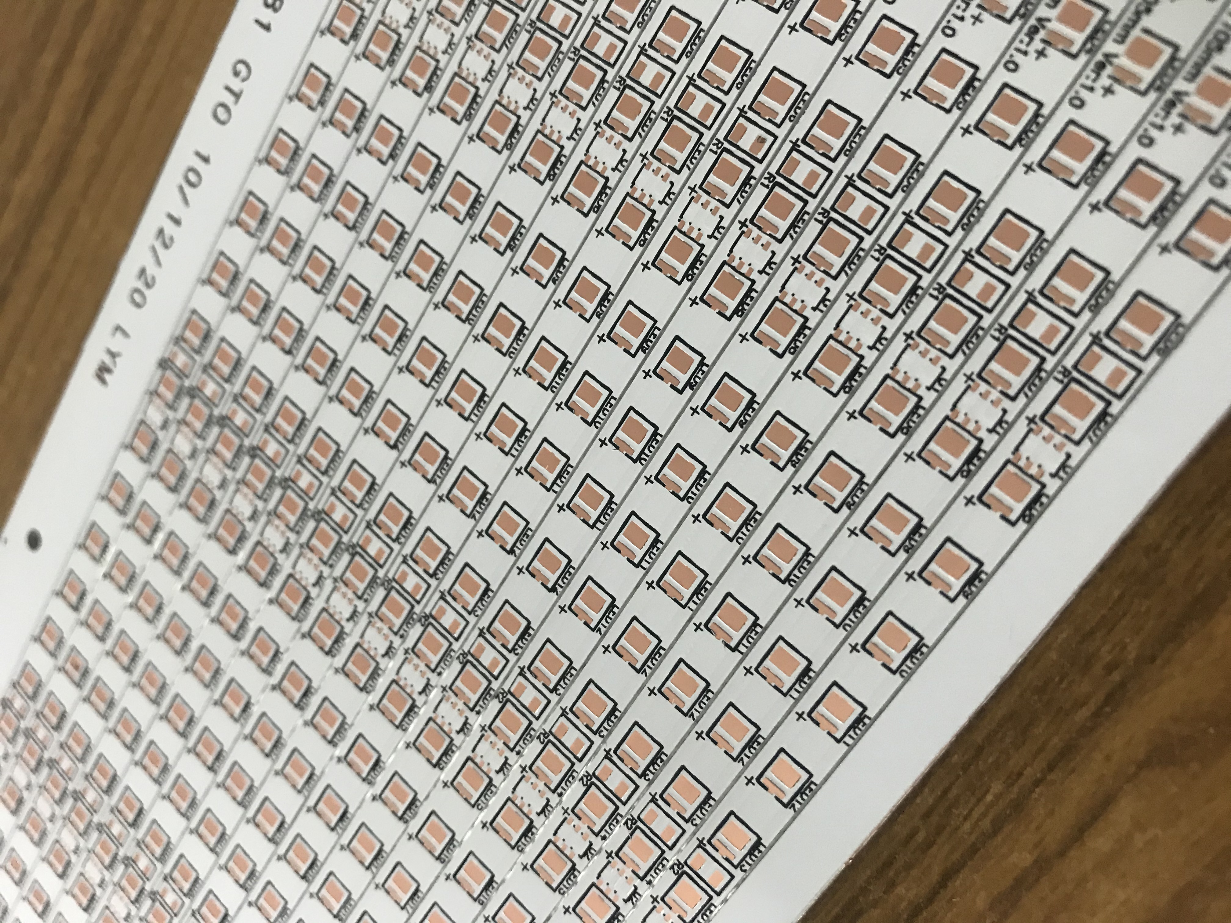
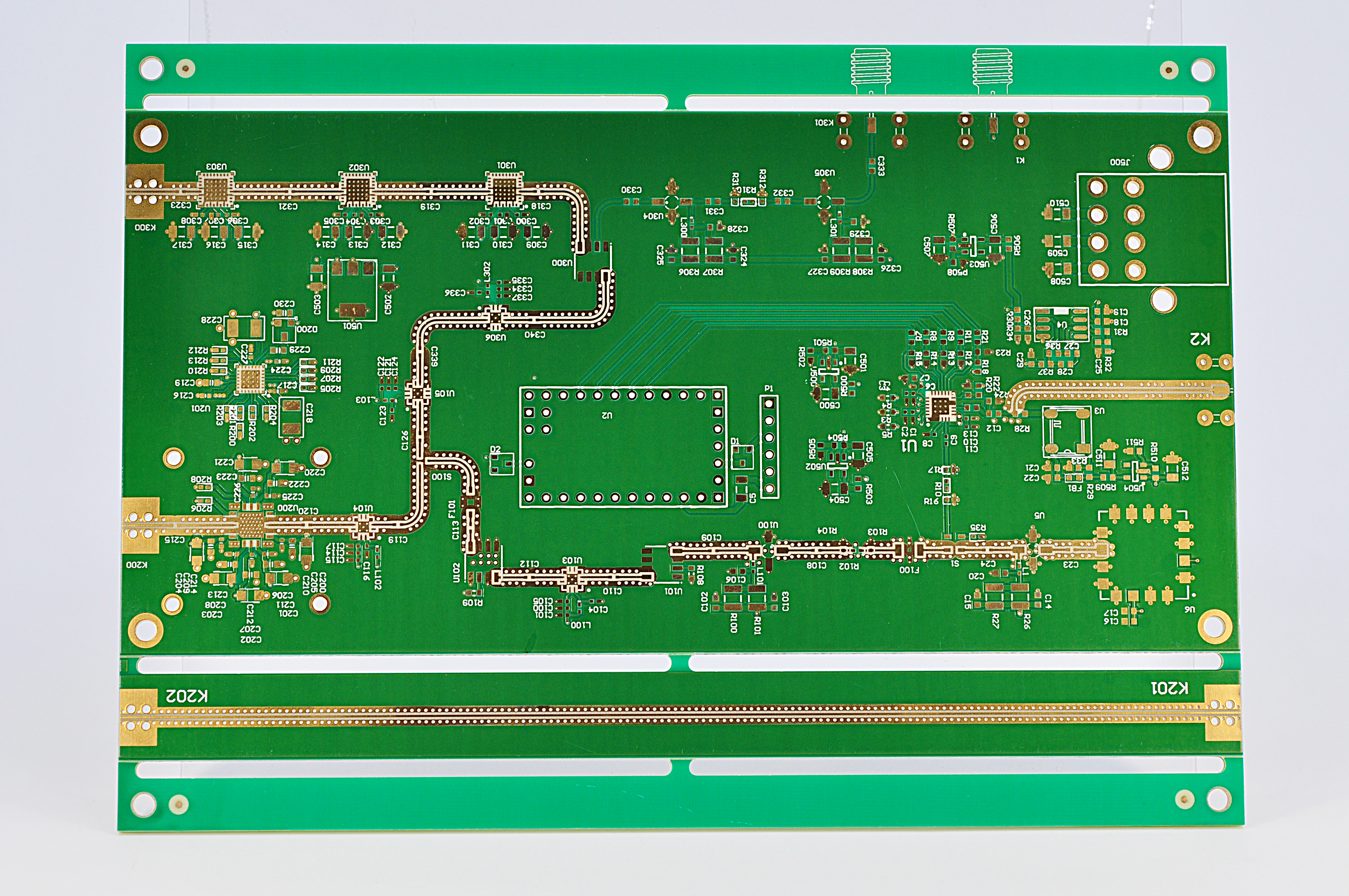
A Guideline about Legend on Printed Circuit Board

November 29th, 2022

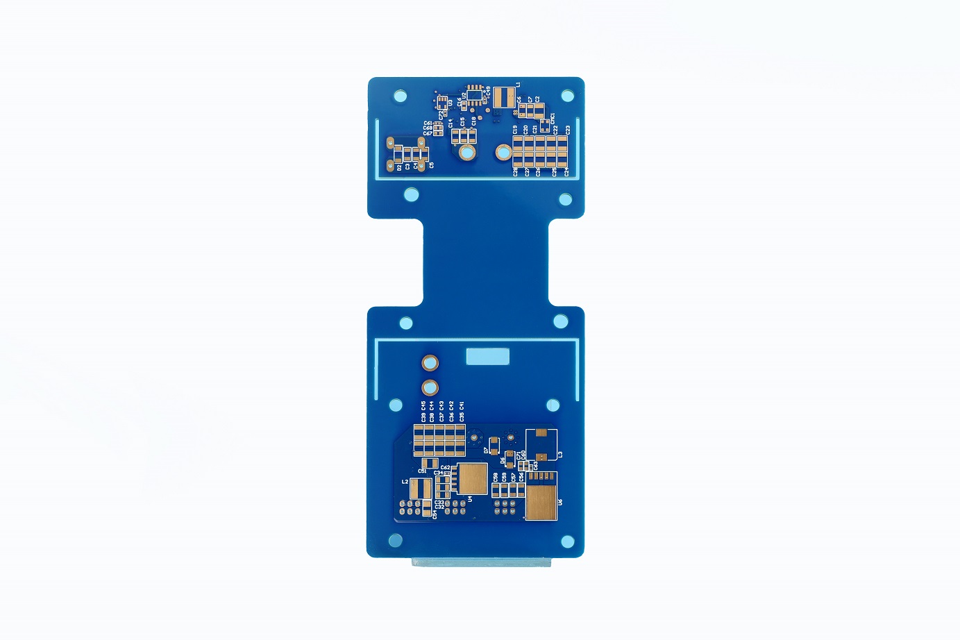
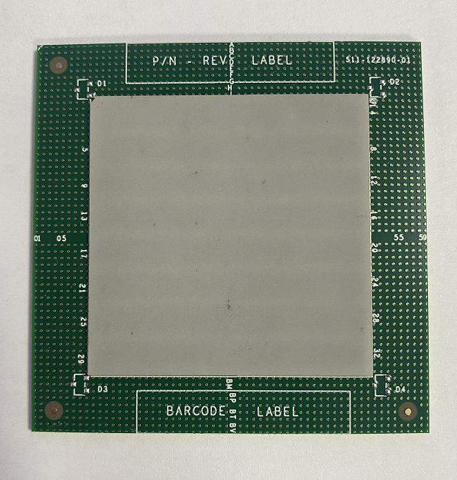
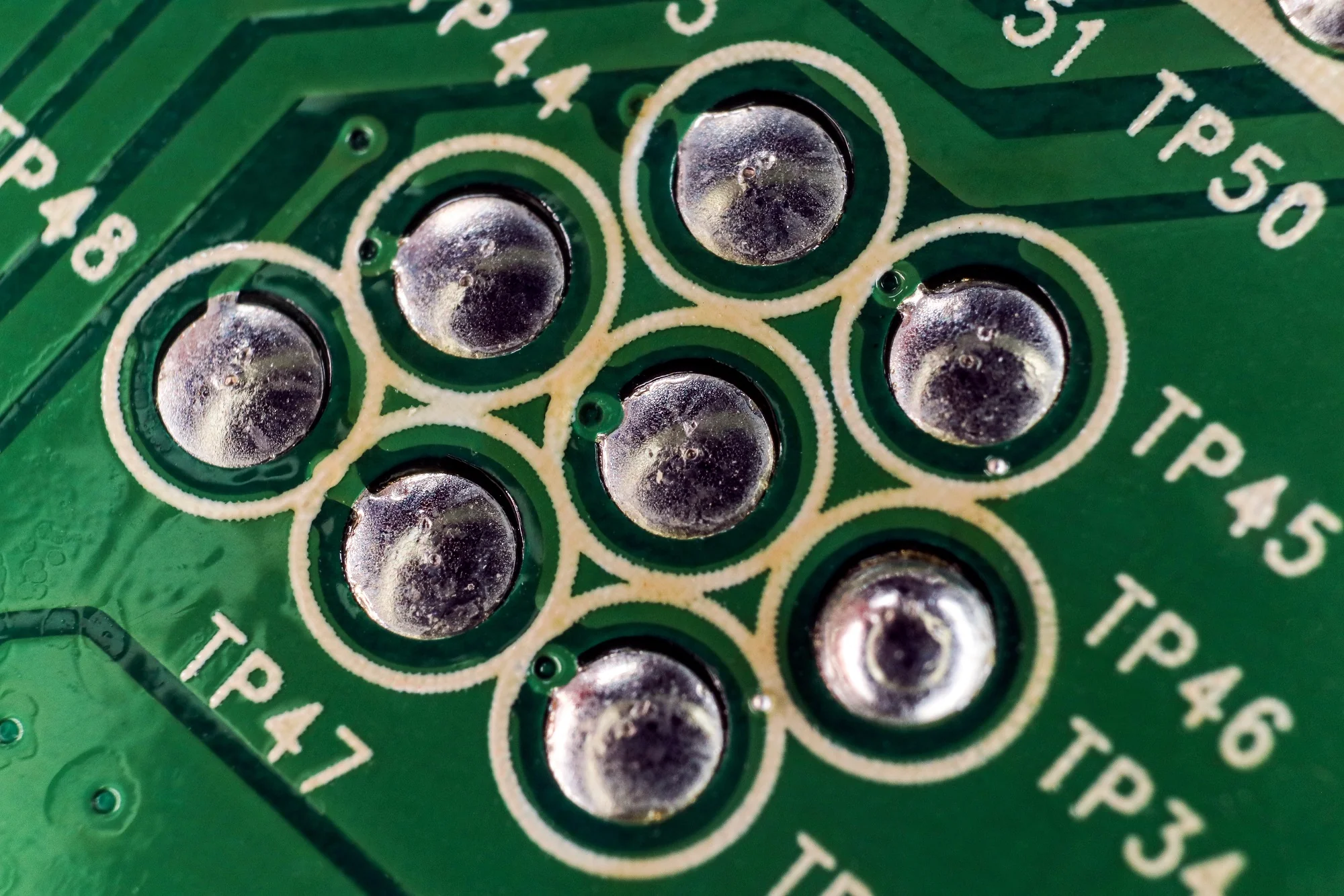
Printed circuit board is used to power up the electronic devices, and the legend on its surface been known as legend text or silkscreen text to be aim at providing vital information to electronic manufacturers or end users. This post is a guideline to help you understand what information we can gain from those legends and what we need to pay attention to when design them.

A brief introduction about PCB legend

Though a printed circuit board doesn’t require any legend/text to function technically, the text provides key information to end users to test, assemble and troubleshoot, and generally we can obtain following information from the legends:

  • Branding information

This includes manufacturer’s information, serial numbers, date code and other information, which prevents the copying of design.

  • Part number provided

Part numbers are added on the circuit boards to enable replacement or design evolution whenever needed.

  • Version of product

Sometimes versions were updated, and the legend is added on the circuits to identify the specific version and backtrack the date.

  • Reference of components indicators

This may feature components information such as indicators, orientations and other information.

  • Safety Precautions

These are warning signals that are added to protect users from electric shocks. A few examples of these may include grounding, high voltage, and so on.

  • Circuit Identification

Users and designers can identify circuit names from legends to understand testing points, ground points, component interconnect, so forth.

  • Polarity indicator for certain components

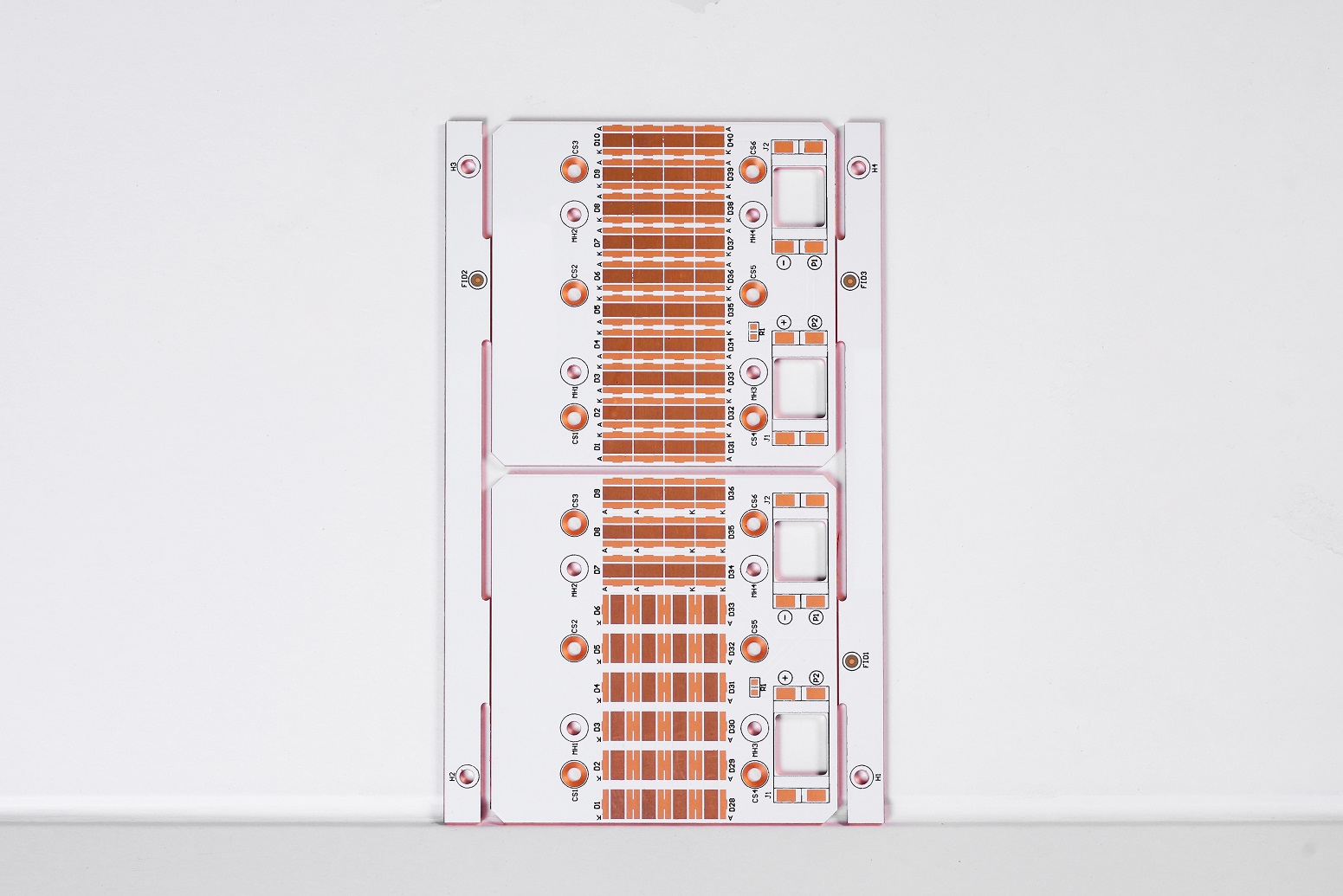
Some components such as diodes, LED chips, electrolytic capacitors require to a distinguish of polarity when assembly, text legends help to indicate the right polarity to ensure assembled correctly and perform functionality when reach to consumers.

  • Authentication indication

Silkscreen text shows the boards are authenticated or conforms to certain security certification, such as RoHS, 94V-0, UL…

  • Test points and troubleshooting assistants

Help to correctly perform testing including resistance measurement, voltage measurement, function testing and so forth.  In addition, text legend enables to troubleshoot while issues or debugs happened and repair is required.

  • Component outlines indicating where components should go

Legends provides a great help during assembly process, it helps the operator quickly find where each component should be, so it is recommended to add text legends when PCB need to be assembled.

General Parameters for PCB Legend in EBest Circuit (Best Technology)

To understand the capabilities of legend printing of EBest Circuit (Best Technology), here we listing some general parameters for your reference:

  • Legend colors can be white, black, green, yellow or other colors depend on customer’s preferences.
  • Legend line width is range from 5mil to 7mil
  • Text height can set at 30mil
  • Maximum text width can be 17mil
  • Printing methods are screen printing, direct legend printing and Liquid photo imaging. (Direct legend printing is commonly used by far.)

Important factors need to be considered during designing

Although legends are easy to be printed, there are still some key points need to pay highly attention when you are designing.

  • Legend orientation: To maintain a good reading appearance for user, please make sure all legends throughout the board have a same orientation.
  • Choose a standard color and shapes for marking, this is a most economy way to save cost.
  • Avoid overlapping: Overlapping is one of the most common problems that manufacturer faced. Legend always be related to PCB layout, and components reference will be also designated when circuit board layout finished. So if the legend was overlapped, it must be moved to another place and that may cause component reference was located in a wrong position, so it is always recommend to double check all the legends, to make sure they are clear and in the correct position when the whole board layout was completed.
  • Do not place the silkscreen text on all four directions, this will lead to confusions when the circuit board is undergoing repair.
  • Leave a few mils space for some common potential printing errors, this will help manufacturer to reduce the possibility of errors.

Every PCB manufacturer has its unique style and pattern when it comes to legend printing, so working files confirmation plays an important role before circuit fabrication, EBest Circuit (Best Technology) gives a great respect to the original files to our customers, we won’t start production until get approval of working files from customers, so please do not worry about it if you have such concerns. In addition, as a professional printed circuit board manufacturer in Asia, we are confident that we can provide you with high quality PCB, welcome to contact us if you have PCB needs.

You may also like

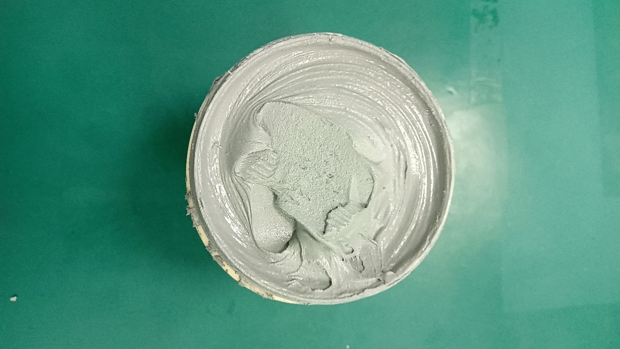
3M Epoxy Adhesive DP190-Gray & 3M Epoxy Adhesive DP190-Translucent

April 22nd, 2022

Both 3M Epoxy Adhesive DP190-Gray and 3M Epoxy Adhesive DP190-Translucent are a two-part epoxy adhesive that delivers exceptional performance with high shear and peel strength.

They can bond to a wide range of materials, such as metals, ceramics, wood, fiberboard, glass, rubber and many plastics. So, PCB is no exception. But what are the similarities and differences between them?

Similarities

  • Provide tough, strong bonds through high shear and peel strength.
  • Capable of bonding to a wide variety of different materials.
  • Deliver extended work-life, providing additional time for adjustment.
  • Exhibit good environmental aging properties, delivering long-term durability.

Differences

3M Epoxy Adhesive DP190-Gray has a moderately high modulus. With a 90-minute work-life, it reaches handling strength in approximately 10 hours and full cure in 7 days at room temperature.

Additionally, this epoxy adhesive has medium viscosity and self-leveling with a 1:1 mix ratio by volume. But its flexibility and elongation are moderate.

(3M Epoxy Adhesive DP190-Gray)

3M Epoxy Adhesive DP190-Translucent has a moderately low modulus. With an 80-minute work-life, it reaches handling strength in approximately 10 hours and full cure in 14 days at room temperature.

It has low viscosity and self-leveling with a 1:1 mix ratio by volume. Additionally, it features high flexibility and elongation.

3M Epoxy Adhesive DP190–Translucent

This is all about the similarities and differences between the 3M Epoxy Adhesive DP190-Gray and 3M Epoxy Adhesive DP190-Translucent. It is supposed that you have known about them.

But if you still have any questions about them or PCB, please feel free to contact us. Because at EBest Circuit (Best Technology), we are fully equipped to handle your PCB manufacturing requirements.

You may also like

Via Tented, Via Filled & Via Plugged

December 20th, 2021

Via Tented, Via Filled (filled with solder mask) & Via Plugged (Via In Pad – Conductive material or Non-Conductive material)

One of the most confused idea during our PCB design is the difference between Via Tenting, Via Filling and Via Plugging. Designers often get mixed up between them and fail to take full advantage of the process.

Today, let us discuss them, so that you can be confident in specifying your design requirements clearly when submitting PCB files to EBest Circuit (Best Technology) before final manufacturing.

Via Tented

What is via?

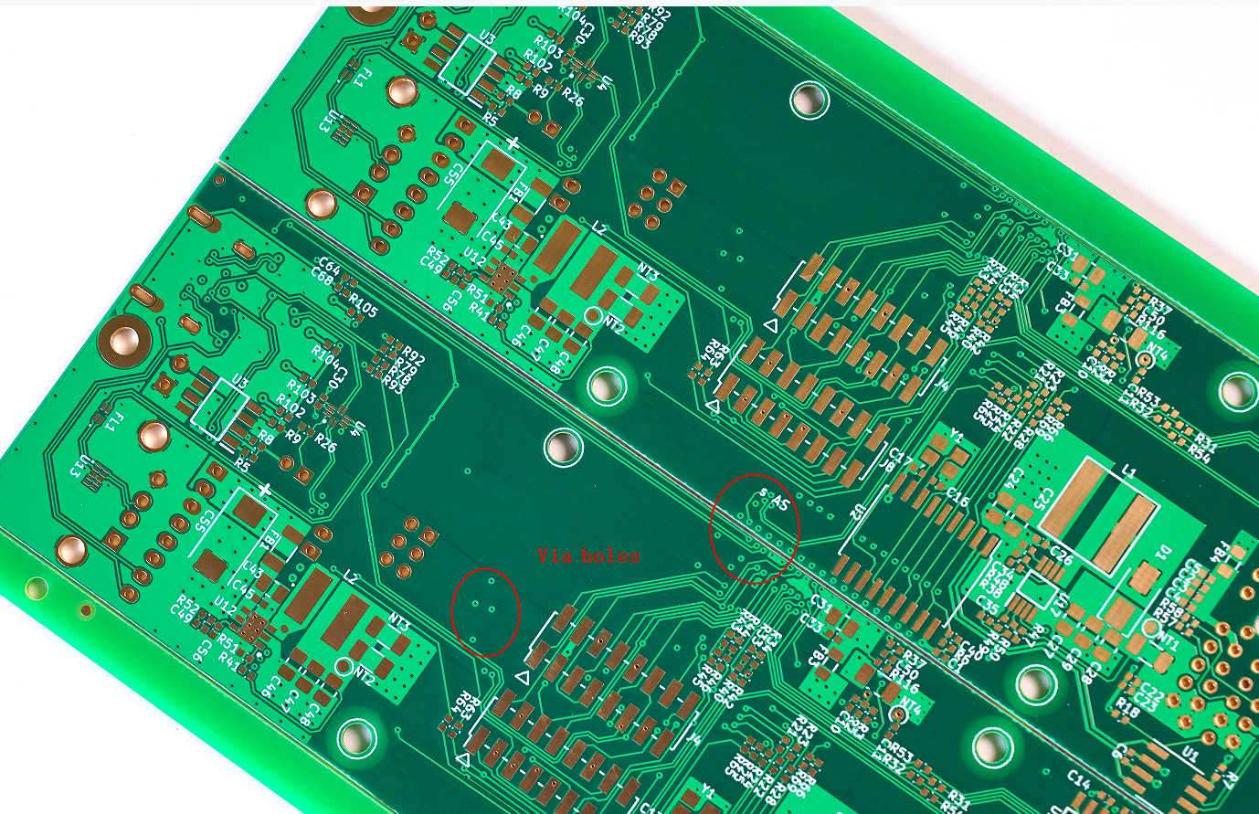
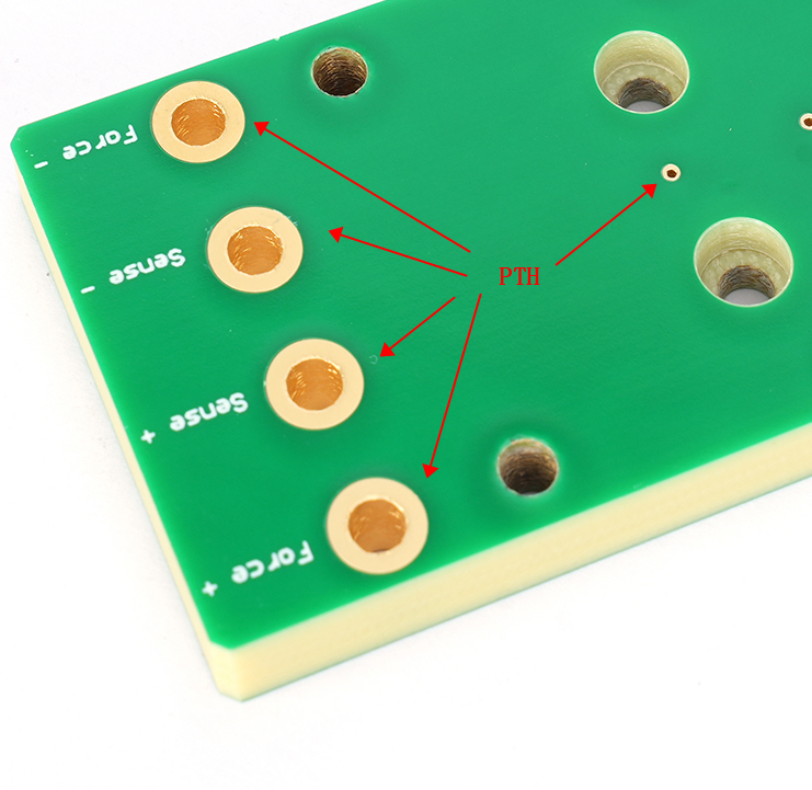
A plated through hole (PTH) in a Printed Circuit Board that is used to provide electrical connection between a trace on one layer of the Printed Circuit Board to a trace on another layer. Since it is not used to mount component leads, it is generally a small hole and pad diameter.

A. Three methods and definitions of via processing

There are three methods for via processing: via hole opening & via hole cover oil & via hole plug oil

1. Through hole opening window: it is the tin on the solder ring of the via (the tin is exposed like a plug-in pad). The window is usually used to debug the measurement signal. The disadvantage is that it is easy to cause a short circuit.

2. Through hole cover oil: it is the welding ring of the through hole (via) covered with solder mask ink

3. Through hole plugging oil: refers to plugging the hole with ink.

Secondly, the inspection standards for a processing method

1. Through-hole opening window is like a plug-in pad, and the window is sprayed with tin. Inspection standard: tin can be tinned, and tin can be easily tinned.

2. The inspection standard of the via hole cover oil: it is not easy to tin in the patch.

3. Inspection criteria for via plug oil: First, it must be opaque, and it must be covered and blocked by ink.

Finally, we are talk for comparison and distinction between via hole cover oil and via hole plug oil:

1. Via plug oil This process is an important supplement to via plug oil, so generally high-quality boards will require via plug oil. And often many engineers who are just entering the industry are stupid and unclear. So how do you distinguish between the two?

2. The requirement of via hole cover oil is that the ring of the via hole must be covered with ink. The emphasis is to ensure the thickness and coverage of the ink on the edge of the hole. The key control is that the ring does not accept false copper exposure and orifice oil. Thin

3. Through hole plugging oil is the production of plug holes with ink inside the holes of the through holes. The emphasis is on the quality and density of the plug holes. After the holes are plugged, no light can be transmitted.

4. The method of plugging the via hole is to first fill the via hole with ink to block the via hole, so that the ink on the solder mask will not flow into the via hole, so as to achieve the situation that the via hole does not appear yellow. (If you have strict requirements and place an order for via hole cover oil, the cover oil is usually not full or yellowish, you can change it to via hole plug oil later). In addition, the smaller the vias are, the easier it is to plug them. The vias of the fortress oil are not easy to be too large (the circuit board proofing plugging oil is directly plugged with ink, and the printing tape is plugged. It is recommended that the vias that need to be plugged are designed to be <0.5mm. This is also free; no additional money is required).

If you have more question Via Tented, Via Filled& Via Plugged, warmly welcomed to contact Best Tech for more FR4 design service.

You may also like

A Brief introduction for different layers on Multilayer PCB

October 29th, 2021

When it comes to multilayer PCB, we know the multilayer PCB are consisted by many different layers. Do you know what’s the purpose for these layers?

Here I would like to give you a brief introduction for the functions of each layer on a Multilayer PCB design.

Mechanical layer: There may be one or several mechanical layers in a PCB depending on the design. There should be at least one mechanical layer as it shows the physical dimensions of the board. Generally, it used GM1, GM2 to name the file on the Gerber.

Solder paste layer: This is a material applied onto the PCB layers where components are mounted, mostly through soldering. It helps with the bonding of the solder with the component pin and improves the solder flow. PCB Assembly supplier will make stencil according to the solder paste layer on the Gerber.

Generally, it used GPS, GBS to name the file on the Gerber.

Solder mask layer: This layer is a mask or a protective coating applied onto the board to prevent damage and contamination. It is typically green in color; however, you can also choose other colors such as blue, black, white depending upon your requirements. Generally, it used GBS, GTS to name the file on the Gerber.

Ground planes and power planes: These are layers for copper, the ground and the power planes are connected to an onboard voltage point. Generally, it used GND, PWR to name the file on the Gerber.

Split planes: This is a modified version of power and ground planes; they are split in a manner that they can be connected to multiple voltage points or potentials.

Keep out layer: This layer is crucial as it defines the working boundary and keeps it separate from the outer mechanical layer. Generally, it used GKO to name the file on the Gerber.

Silkscreen layer: This is typically the text displayed on the boards through which you can identify components with their names. It is typically white in color when solder mask color is green, black, blue and red. But you can also choose other colors such depending upon your requirements. Generally it used GTO, GBO to name the file on the Gerber.

Routing layer: These layers help to interconnect the components. They can also be present on the top and bottom layers of the board.

Drilling Layer: This is the layer to show the drilling information of the PCB. Usually, it names DRL on the Gerber.

Once we understand the purpose of each layer for PCB, then understanding the construction of PCB becomes easy, no matter how complicated the board structure.

With over 15 years of PCB manufacturing experience, BEST Technology can meet different requests from customers no matter it is prototype or high-volume PCB.

Send us your request, let us to make the high-quality printed circuit boards for you.

You may also like

About the “heat” problem in PCB & MCPCB

October 18th, 2021

For high-power products, the concept of “heat” is often mentioned, which is especially important in high-power products. It not only determines the service life of the product, but also relates to whether the product can work properly.

We will explain the “heat” problem in circuit board design from three aspects: the generation of heat, the impact of heat on the product and the “heat” in the system layout.

1. Heat generation:

Heat generation in a system takes several paths:

1) Power consumption of the component itself

2) Efficiency of power conversion devices

3) High frequency signal conversion heating

4) Power consumption of contact resistance and wire resistance during signal transmission

2. Impact of fever on products

The operating temperature of components is generally below 80 degree, and the operating temperature of commonly used capacitors and resistors is generally controlled below 50 degree. If the temperature of the system is not controlled, the following conditions may occur:

1) The temperature rise will cause the working parameters of components to change, resulting in the unstable working performance of the whole system.

2) Temperature rise will accelerate the aging of components, affecting the accuracy and life of components.

3) Temperature rise will cause circuit board deformation and poor connection of components.

General heat dissipation components arrangement

3. “Hot” considerations in system layout

1) Selection and layout of the chassis: choose materials with good thermal conductivity, such as aluminum alloy

2) Black heat absorbing material is coated inside the shell to enhance the function of radiation heat absorption

3) The shell is closely combined with the components with high calorific value to conduct heat dissipation

4) A large number of heating components should be placed at the edge of the plate to shorten the heat transfer path. Heat-resistant components should be kept away from light sources.

5) In the design process, the appropriate wire width and copper thickness should be selected, and the influence of wiring density on the current-carrying capacity should also be considered. Copper foil should be filled in the gap of the board surface as far as possible for heat conduction. The heat conduction hole can help effectively heat dissipation and reduce local temperature.

In the design of circuit board, how to effectively control the temperature of the system is a problem that must be considered.

You may also like

The function of solder mask layer on the PCB Board.

September 20th, 2021

At last time, we shared a blog talking about Why most of the PCB boards are green?. Believe you’ve known the reasons for why most of solder mask colors are green.

Today, let’s share something about the function of solder mask on the Printed Circuits Boards.

The solder mask layer is designed mainly to prevent the PCB copper foil from being directly exposed to the air and play a role in protecting the PCB surface, which is also to prevent the area that should not be soldered from being soldered.

PCB Solder mask

As we know that almost all the PCB need to do the assembly, which need to go through the reflow soldering while the assembly, and solder mask plays an important role during control of the reflow soldering process.

Here is a summary for what solder mask roles played on the board:

(1) Prevent physical disconnection of conductor circuits on the circuits board;

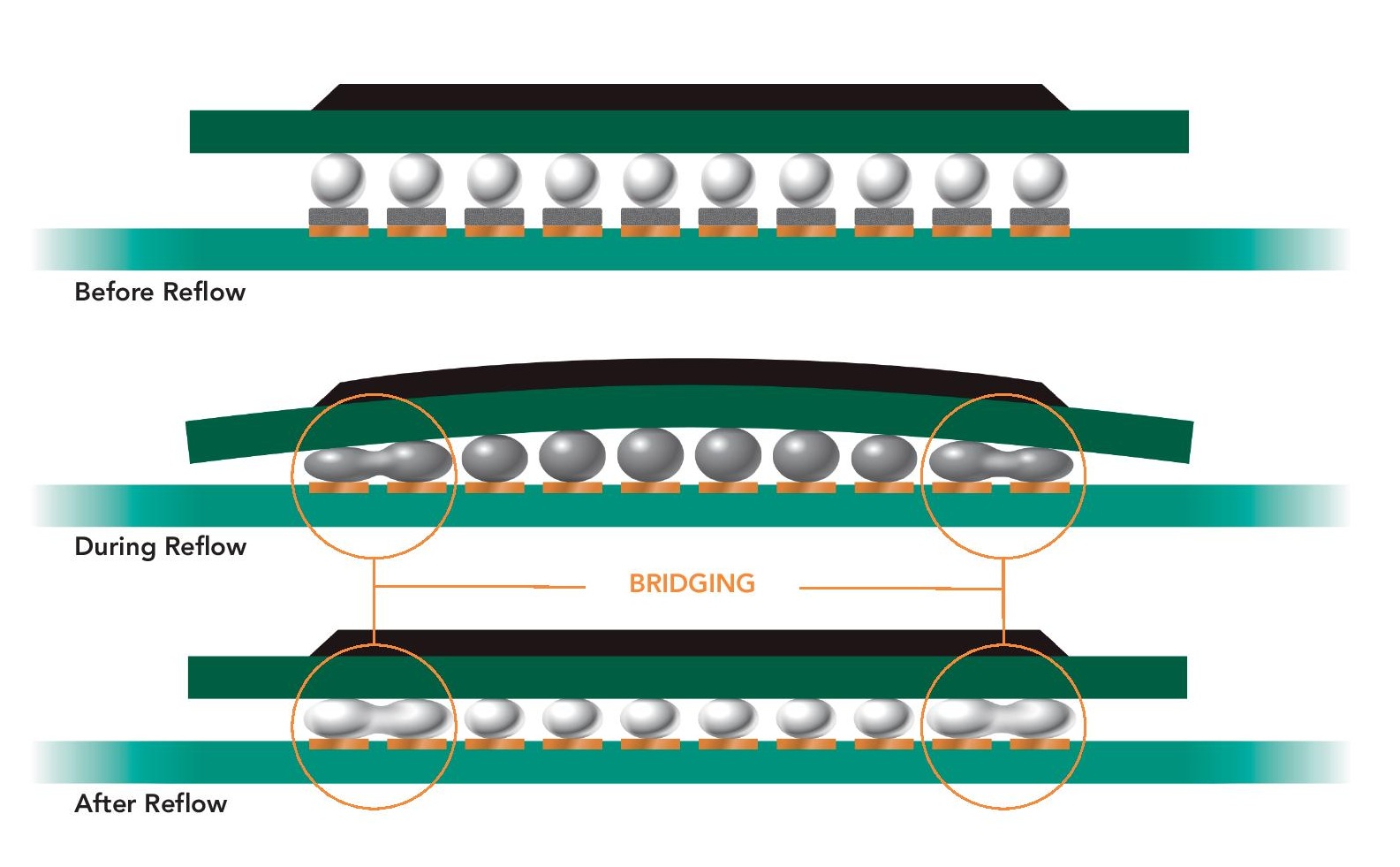
(2) In the welding process, solder mask can prevent short circuit caused by bridging;

(3) solder mask can reduce copper pollution to the soldering trough;

(4) Print solder mask on the PCB can prevent insulation deterioration and corrosion caused by external environmental factors such as dust and moisture;

(5) Solder mask are with high insulation; it is possible to increase the density of the circuit.

Red solder mask

In terms of solder mask material, it must be used through liquid wet process or dry film lamination.

Dry film solder mask materials are supplied in a thickness of 0.07-0.1mm (0.03-0.04″), which can be suitable for some surface mount products, but this material is not suitable for PCBs with tighter pitches.

You may also like

Why most of PCB boards are green?

August 24th, 2021

You may have found such a situation, most of the PCB boards are with green colors, while other colors are relatively rare to see, do you know why?

As we know that the Printed Circuits Board consists of Solder Mask Layer, Silk screen layer, solder PAD, Copper traces, surface finishing and other parts, etc.

Among them, the solder mask refers to the part of the PCB that is covered by oil. Since most PCB boards use green oil, the part of the green oil that can be seen on the board surface is the solder mask, which play an important role during the reflow soldering process.  

green solder mask

Then why are most of the PCB boards green? The main reasons are as follows:

  1. Green is less irritating to the eyes. We all know that green is good for the eyes and can resists fatigue. So when the PCB board with green solder mask, relative production and maintenance personnel are not prone to eye fatigue when staring at the PCB board for a long time, and it is less harmful to the eyes.

2. Cost for Green oil is lower. Since green is the mainstream in the production process, the purchase of natural green oil will be larger, and the purchase cost of green solder mask will be lower than other colors. At the same time, using the same color oil in mass production can also reduce the replacement cost.

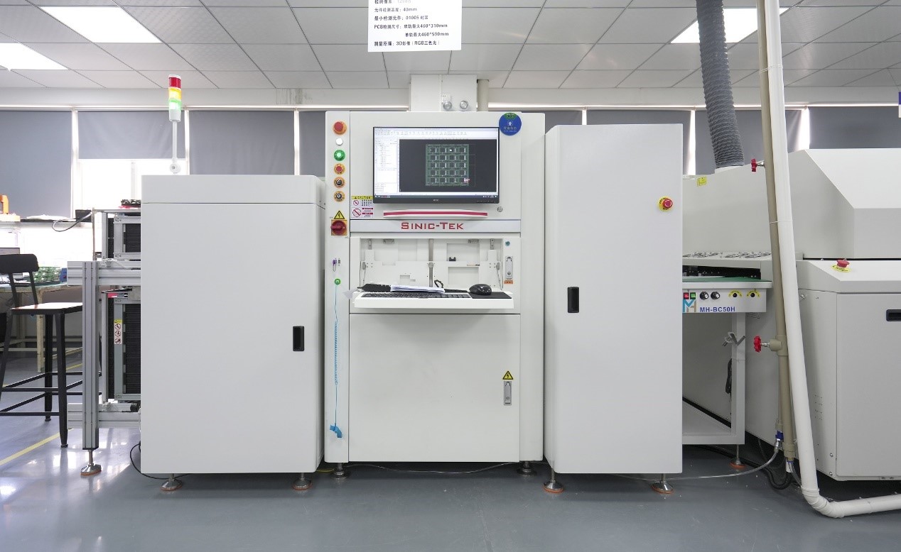
  • When the board works on the SMT soldering process,  it needs to go through the process from Tinning, post soldering and final AOI inspection. These processes all need to be optically positioned and calibrated. The green background color is better for the recognition of the instrument.
PCBA AOI testing

Okay, now, do you understand why most of PCB boards are with green colors?

Though we know green is the most common one, but other colors such as red, yellow, blue, purple, black or some other colors are okay for us to make.

solder mask colors

If you have PCB board with a special color want to make, please contact us and we will try best effort to meet your request.

You may also like

What kind of test for Coil Printed Circuit Board?

August 11th, 2021

In year 2019, one of our US customers asked us, Marina can EBest Circuit (Best Technology) make a Coil PCB (Printed Circuit Board) with FR4 material? Yes, of course, we can make different kinds of PCB for our customer, included for the Coils PCB, which currently is widely used for wireless charging and antenna products. Please see the following Coils board from EBest Circuit (Best Technology).

The manufacturing process is same as other PCB manufacturing process, and just make sure the etching process and pay attention for the etching tolerance of the coils trace. And when coils PCB board finished, do you know what kind of test need to do to check the functional of Coils boards?

Today I would like to share how EBest Circuit (Best Technology) test Coil PCB board. Everyone knows that we check the quality of PCB board with Flying probe tester, as the production efficiency is extremely low and the inductance and capacitance cannot be accurately measured. In this way, we need to use LCR meter to make verify the inductance and capacitance. See the LCT meter as following.

EBest Circuit (Best Technology) chooses the digital meter LCR Meter to test the impedance characteristics of the coil. From the LCR tester you know see two numbers, one for inductance and another for resistance.

After test each coils printed circuit board, we will make record at our paper to make sure every measurement data will meet for customer requirement.

Currently, LCR Meter only provides a single-channel test function, and can only test the impedance characteristics of a set of coils at a time. But this is the effective test method for Coil printed Circuit Board. But we believe we will buy more LCR meters to let the test coil board become quicker.

If you have any comments on the testing for Coil printed circuit board, you are welcome to send us query and we are happy to discuss with you. You can visit www.bestpcbs.com to know more about us. Thank you

You may also like

What is E-Tester for Printed Circuit Board?

July 11th, 2021

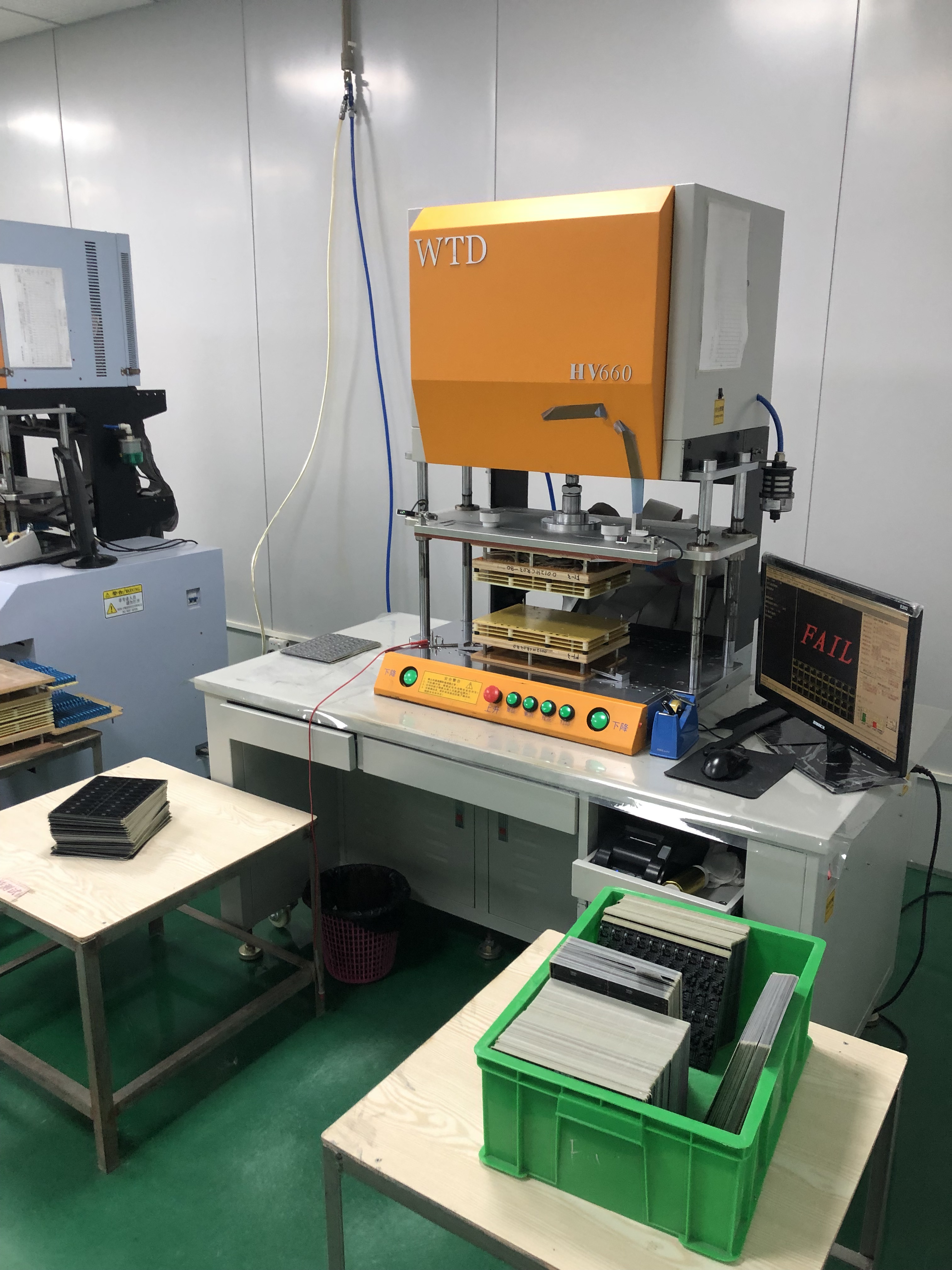
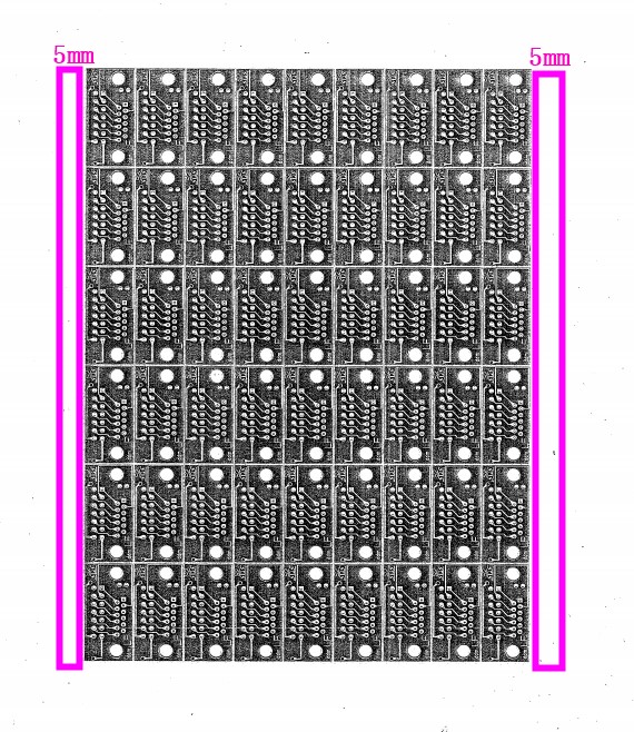
When the bare Printed Circuit Board qty become volume fabrication, the PCB manufacture will not use the Probe flying tester to test the PCB circuit board. Best Tech will make new PCB test fixture to test the bare PCB, The electrical Test (E-test), which is the final electrical test to verify net continuity and the absence of shorts on the bare printed circuit boards (PCBs). In Best Tech PCB factory, we perform 100% electrical testing on all bare PCBs its facilities as per IPC-6012 class 2 standard. And from the following photo in computer, you can see it will show PASS for PCB.

in test

in test

To test the PCB boards, we require the NETLIST file. Normally we create a reference netlist file from the customer’s original Gerber files during PCB fabrication.

We always prefer to receive the CAD file based on the netlist for comparison. Since a CAD based netlist is generated before PCB routing, it provides another layer of checking (against the Gerber files). This allows us to catch any PCB faults introducing in the event of an error in the Gerber files. For full turnkey PCB assembly (PCBA service) projects, this helps to ensure that the PCB boards are 100% correct before any components are populated.

tester 2

tester2

Here are Best Tech E-tester Capabilities

Minimum Continuity Resistance0.1 Ohms
Maximum Test Voltage1000 Volts
Max Isolated Resistance25 M Ohm – 2 G Ohm
Electrical Test Pitch (Fixture)20mil(0.5mm)
Electrical Test Pitch (Flying Probe)4mil
Debug /check for missing pins: (Test fixture)10 minutes
Test time per board:40 seconds
Setup time:30 minutes

All points are tested simultaneously. However, this process involves set-up to create the fixture itself and additional costs associated with the cost of materials.

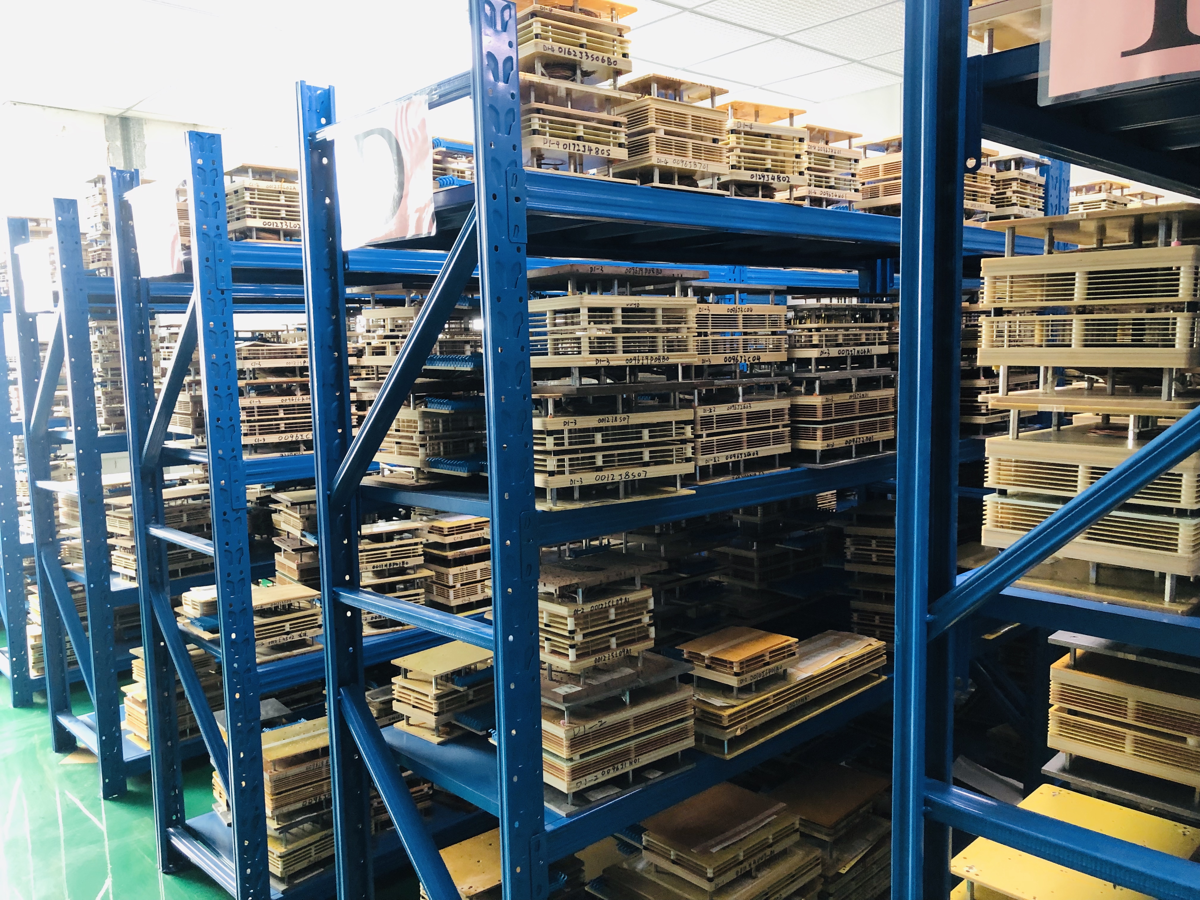
The electrical test fixture has a limited shelf life and repeat using times. For every PCB it will need a fixture and its custom-made for a customer only. Many other factories only store 2 years shelf life for electrical test fixtures, but Best Tech will store at least 3 years for customer.

In order to ensure the quality of fixtures and spare enough space to store fixtures, Best Tech leaves one floor to keep the fixture. See attached fixture photo.

tester 1

tester1

During the 3 years’ time, customer no need to pay the fixture charge again if the update is no update. The flexible test fixture shelf-life policy, it will help customer save the cost.

At the end of the PCB production process, we use electrical test to check the interconnectivity of the PCB is correct against the original board data.

Best Tech did the E-Tester to test the PCB 100% before delivery to customer, this makes Best Tech get highly comments from our customer on the world with good printed circuit board quality and best service. See the customer highly comments of Best Tech.

customer highly comments on our service

customer highly comments on our service

You are warm welcomed to contact Best Tech to discuss about the Printed Circuit Board (PCB).

You may also like

What is IPC standard for PCB?

June 28th, 2021

Do you know what is IPC standard for PCB?IPC, it is a trade association whose goal is to standardize the assembly and production requirements of electronic devices and components.  It was established in 1957 as the Institute of Printed Circuits.  IPC has developed thousands of standards and specifications to regulate the electronics manufacturing industry.

IPC standards are related to PCB design, production technology, electronic assembly, etc., in order to achieve high reliability, high quality, high performance, and meet user specifications.

What are the IPC Standards for?

Before we can understand IPC standards, we first need to know who made them. It comes from the IPC Association, a trade association whose goal is to standardize assembly and production requirements for electronic devices and components. It was founded in 1957 as the Printed Circuit Research Institute. Its name was later changed to the Institute for Electronic Circuit Interconnection and Packaging to highlight the expansion from bare boards to packages and electronic components. In 1999, the organization officially changed its name to IPC with the slogan “Association Connecting Electronics Industries”.

What is IPC standard for PCB?

IPC standards are the most widely recognized code of acceptability in the electronics industry. The organization publishes standards for nearly every stage of the electronic product development cycle, including design, procurement, assembly, packaging, and more. In other words, IPC standards refer to everything in the electronics industry and are the basic knowledge of designers and manufacturers.

Just like the IPC standards tree, there are many different aspects of standards that all serve the end product. IPC-A-610, for example, focuses on the acceptability of electronic components and is used worldwide by original equipment manufacturers and EMS companies.

What is the PCB IPC Standard?

IPC plays a vital role in the PCB industry by establishing standards that cover every stage of PCB production from design to manufacturing. These standards ensure consistency and compatibility throughout the PCB process. During the design phase, IPC standards guide file formats, PCB design software, design guidelines, and electronic product documentation. They also affect the material selection of PCB components, surface mount equipment and surface treatments. In addition, these standards are essential for testing and evaluating the acceptability of printed boards.

When it comes to welding, IPC standards cover a variety of techniques, including reflow soldering, wave soldering and welding. These guidelines help companies determine whether their electrical and electronic components meet quality expectations during manufacturing. IPC standards also address cable and harness assemblies to ensure they meet standards.

The most widely recognized IPC standard for PCBs is IPC-6011, which Outlines the performance requirements for PCBS. However, IPC-6012 is more specific and governs the qualification and performance of rigid PCBs. IPC-6012 covers everything from how the PCB should be made to its thickness and the integrity of the copper layer. Compliance with this standard ensures that PCBs meet electrical and mechanical performance expectations. Whether you’re creating boards for high-end computers or small consumer devices, compliance with PCB IPC standards is critical to meeting industry and customer expectations. Here is the IPC tree for your reference:

What is IPC standard for PCB?

What is the IPC Level of PCB?

One of the most widely used industry standards in the manufacturing of printed circuit boards is IPC-A-610C Acceptability of Electronic Assemblies and IPC-A-600 Acceptability of Printed Boards. This standard is used primarily for the incoming inspection of bare boards from a PCB fabricator.

In the IPC-A-610C document, electronic products are divided into level 1, level 2, and level 3. The higher the level, the stricter the quality inspection conditions. Here are how 3 levels divided:

Level 1 products: called general-purpose electronic products. Including consumer electronic products, certain computers and their peripherals, and products whose main purpose is to use functions.

Level 2 products: called dedicated service electronic products. Including communication equipment, complex industrial and commercial equipment and high-performance, long-life measuring instruments. Under normal use environment, this kind of product should not malfunction.

Level 3 products: called high-performance electronic products. Including high-reliability, long-life military and civilian equipment that can continue to operate. This kind of product must not allow any interruption failure during use, and at the same time, it is necessary to ensure the reliable startup and operation of the equipment in a harsh environment. Such as medical life-saving equipment and all military equipment systems.

For PCB manufacturing, do you know which IPC standards are commonly used?

What is IPC standard for PCB?
multilayer pcb

IPC Standard for PCBs

The IPC has created several standards for printed circuit board (PCB) design, manufacturing, and assembly. Here I would like to share you some standards which we mainly use:
  • IPC-2221

A general standard that covers almost every aspect of PCB design, including electrical considerations, thermal design, and manufacturing-ready design.

  • IPC-2222

A guide for rigid PCB cross-sectional design, including recommendations for board thickness, hole aspect ratio, and dielectric clearance.

  • IPC-2223

A standard for reliable Flex-PCB design, including guidelines for material selection, impedance control, and pad placement.

  • IPC-2224

A standard for PC card form PCBs, including design requirements for organic and inorganic materials, and single, double, or multilayered interconnections.

  • IPC-A-610

A standard for PCB assembly that classifies PCBs into three quality levels, with Class 1 being the lowest and Class 3 being the highest.

  • IPC-6011

General Performance Specification for Printed Boards

  • IPC-6012

Appraisal performance and specifications for Rigid printed boards

  • IPC-6013

Appraisal performance and specifications for Flexible printed boards

  • IPC-6016

Fixed performance and specification of HDI or printed circuit board of high density interconnection layer

  • IPC-SM-840

Appraisal and performance of permanent performance

  • IPC-HM-860

Multilayer Hybrid Circuit Specification

  • J-STD-003

Solderable test for printed boards

  • IPC-A-600F

Acceptance conditions for printed boards

  • IPC-4761

Design Guide for Protection of Printed Board Via Structure

What is IPC standard for PCB?
resin filled production bpm20599

What is IPC-A-610 Standard?

IPC-A-610 Standard is one of the most widely recognized standards in the electronics industry, specifically focusing on the acceptability of electronic assemblies. It provides detailed guidelines and criteria for the inspection of PCB assemblies, so that these assemblies meet the necessary quality levels for their intended use. Its main content includes:

1. Soldering Criteria

IPC-A-610 provides in-depth guidelines on acceptable soldering techniques, covering solder joints, surface mount devices (SMDs), through-hole components, and wire terminations. It explains what constitutes an acceptable versus defective solder joint, ensuring that the electrical connections are reliable.

2. Component Placement

The standard includes criteria for the correct placement and alignment of electronic components on PCBs. It specifies the acceptable tolerances for misalignment and ensures components are correctly placed for proper electrical performance and physical integrity.

3. PCB Assembly Defects
IPC-A-610 details different types of assembly defects, such as insufficient solder, tombstoning, lifted pads, and more. Each defect is categorized based on its severity and impact on the function and reliability of the product, providing guidance on whether a defect can be accepted or if it requires rework.

4. Classes of Electronic Assemblies

The standard divides electronic assemblies into three classes based on the end-use of the product:

  • Class 1 – General electronic products
  • Class 2 – Dedicated service electronic products
  • Class 3 – High-performance products

5. Mechanical Assembly

IPC-A-610 provides criteria for the mechanical aspects of PCB assemblies, such as mounting hardware, screws, connectors, and wire routing.

6. Coating and Potting

The standard covers the application of protective coatings (conformal coatings) and potting materials that protect the PCB from environmental damage such as moisture, dust, or chemicals. It specifies acceptable thicknesses, coverage areas, and inspection methods.

7. Cleaning Requirements

The cleanliness of PCB assemblies is critical for preventing performance degradation over time. IPC-A-610 outlines acceptable levels of residues from fluxes and other contaminants and specifies methods for inspecting and verifying cleanliness.

8. Cable and Wire Harness Assemblies

The standard includes requirements for assembling and inspecting cable and wire harnesses.

9. Solderless Wire Wraps

The standard also touches on solderless wire-wrapped connections, which are used in some applications where soldering is not practical or preferred. IPC-A-610 defines the acceptable criteria for such connections.

10. Inspection and Testing

    The IPC-A-610 standard provides guidelines for visual inspection and testing methods used to evaluate whether an assembly meets the required acceptability criteria. This can include both automated and manual inspection processes, depending on the class of product.

    Why IPC Standard is Important?

    IPC standards are of great importance to the circuit board industry.

    1. IPC standard specifies the requirements for all aspects of the design, manufacturing and assembly of the circuit board, including material selection, size specifications, welding quality, reliability testing, etc., providing a unified reference and guide for circuit board manufacturers to improve product quality and reliability.

    2. IPC standards can help communicate and cooperate between PCB manufacturers and customers. By referring to IPC standards, the two parties can reach a consensus on PCB specifications, quality requirements and other aspects, reduce misunderstandings and disputes, and improve production efficiency.

    3. For customers, IPC standards provide confidence. When a company adheres to these standards, they can trust that the final product will be reliable and durable, even in demanding environments.

    4. In addition, IPC standards also contribute to the technological innovation and development of the circuit board manufacturing industry. By being in line with international standards and understanding the latest technological trends and standard requirements, manufacturers can continuously improve production processes and equipment, improve production efficiency and product quality, and enhance competitiveness.

    At the same time, IPC regularly updates and revises standards to meet changing technology and market needs.

    What is the IPC Standard for PCB Clearance?

    PCB clearance, or the distance between conductive components, is essential to avoid electrical shorts or interference. Without proper clearance, electrical shorts could occur, potentially leading to device failure or safety hazards. The IPC-2221 standard covers PCB design and provides guidelines for this clearance, ensuring safety and functionality. This standard specifies how much space is needed between traces, pads, and other conductive materials depending on the operating voltage. However, the minimum clearance between any two conductors on a PCB depends on the device’s intended use and voltage: 

    • General-purpose devices: 0.1 mm (4 mils) 
    • Power conversion devices: 0.13 mm (5.1 mils) 
    • Class 2 and 3 PCBs: 0.25 mm (10 mils) for low voltage and 0.5 mm (20 mils) for high voltage 
    What is IPC standard for PCB?

    What are the IPC Standards for PCB Repair?

    PCB repair can be tricky, but IPC-7711/7721 offers guidance on how to properly rework and repair PCBs. These standards provide detailed procedures for everything from removing defective components to repairing damaged traces and soldering issues.

    By following IPC-7711/7721, technicians can restore a PCB to its original condition without compromising its performance. This is critical in industries where PCBs are expensive or difficult to replace, such as aerospace and medical devices. Repair standards also reduce the environmental impact by extending the life of the PCB, making repairs more sustainable.

    It is no problem for us to manufacture the PCB following the standard in IPC 6012 /6013 Class 2 and Class 3, as well as following to the standard listed above. These acceptance conditions are the basis for the inspection of our company’s products, as well as the working standards of the employees at the production site, and also become an important part of the training of the employees for PCB production and assembly in our company.

    Send us your PCB drawing, let’s help to make your PCB design into a real board.

    You may also like