In the ever-evolving realm of printed circuit boards (PCBs), High-Density Interconnect (HDI) technology stands out as a game-changer. HDI PCBs have revolutionized the electronics industry by enabling the creation of smaller, lighter, and more advanced electronic devices. In this blog, let us delve into the captivating world of HDI PCBs, exploring their unique processes and craftsmanship. We also attached some photos for your ref.

What is HDI PCB?
HDI PCBs, short for High-Density Interconnect PCBs, are a specialized type of circuit board designed to accommodate a higher number of components within a smaller footprint. Unlike traditional FR4 PCBs, HDI boards incorporate intricate designs and advanced manufacturing techniques to achieve denser routing and interconnections.
- Miniaturization and Component Density
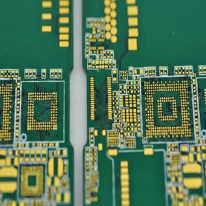
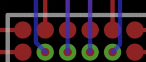
One of the standout features of HDI PCBs is their ability to achieve significant miniaturization. There are fine-pitch traces, microvias, blind and buried vias. You can see the below photo, there are many kinds of the vias.

HDI boards allow for more compact layouts and increased component density. This makes them ideal for applications where space is a premium, such as smartphones, tablets, wearables, and medical devices.
- Advanced Manufacturing Techniques
Creating HDI PCBs involves a sophisticated blend of state-of-the-art manufacturing processes. These techniques include laser drilling, sequential lamination, and advanced imaging technologies. Laser drilling enables the creation of microvias, which are tiny holes used for interconnection between different layers of the board. Sequential lamination involves bonding multiple layers together, creating a compact stack-up with enhanced electrical performance. Advanced imaging technologies ensure precise alignment and accuracy during the fabrication process.
Benefits of HDI PCBs
HDI PCBs offer a multitude of advantages that make them highly sought after in today’s electronics industry:
1. Improved Signal Integrity: With their reduced parasitic effects and shorter signal paths, HDI boards provide superior signal integrity and enhanced electrical performance.
2. Increased Reliability: HDI PCBs minimize the risk of failures due to reduced interconnection lengths, better thermal management, and enhanced impedance control.
3. Enhanced Thermal Efficiency: The compact design of HDI boards allows for better heat dissipation and thermal management, ensuring optimal performance of heat-sensitive components.
4. Design Flexibility: HDI technology opens up new design possibilities, enabling engineers to create innovative and compact product designs without compromising on functionality.
Applications of HDI PCBs
The versatility of HDI PCBs makes them indispensable in various industries, including:
- Consumer Electronics: Smartphones, tablets, laptops, and wearable devices.
- Automotive Electronics: Advanced driver assistance systems (ADAS), infotainment systems, and autonomous driving technology.
- Medical Devices: Miniature medical implants, diagnostic equipment, and patient monitoring systems.
- Aerospace and Defense: Avionics, satellites, and military-grade electronics.
- Industrial Automation: Robotics, control systems, and IoT devices.
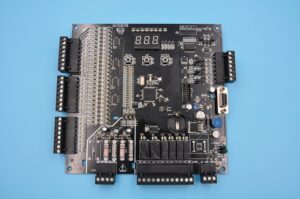
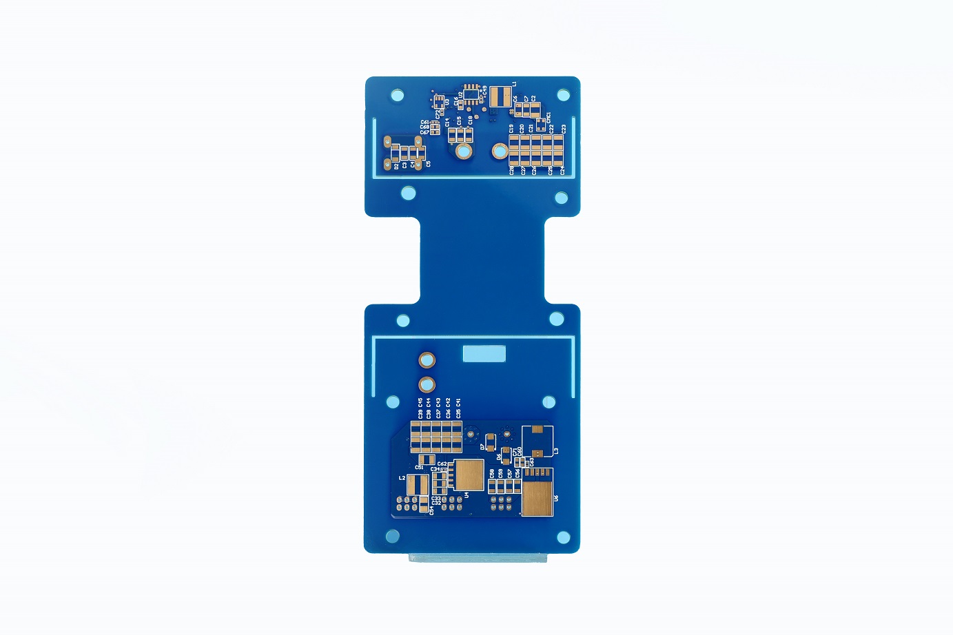
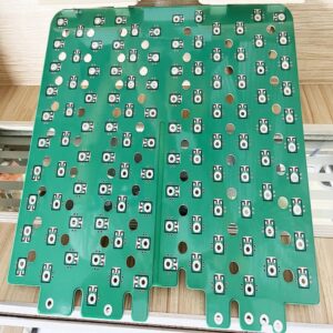
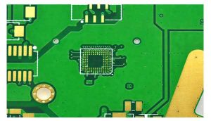
We have many customers from various industries, the PCBs of the below photos are what we produced for our customers.


Conclusion
As technology advances, HDI PCBs will undoubtedly play a crucial role in driving innovation and pushing the boundaries of what is possible in the world of electronics.
We hope this exploration into the captivating world of HDI PCBs can make you know more about HDI PCB. If you’re interested in any HDI PCB, please feel free to contact us any time. Let us supply you an excellent solution and awesome boards for you.


