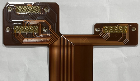
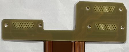
Recently, Best Technology faced a huge challenge in a 2oz copper rigid flex PCB manufacturing, this board appeared simple on the drawing but revealed multiple layers of engineering challenges once entering mass production. But finally, we finished this project very well and overcome this challenge, letâs see what are the challenges on this project and how does our team overcome them!
Project Introduction
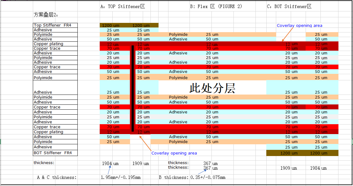
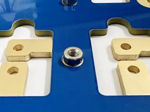
The board used a 70/25 double-sided adhesive ED flexible substrate with PI25/AD50 coverlay, coupled with a 2+2 layers dual access structure that required thick copper, small annular rings, narrow spacings, and FR4 stiffeners with extremely limited clearance. Each of these parameters independently creates difficulty, but combined, they demand precise collaboration between engineering, fabrication, and process control.
This article explains:
Why the design was inherently difficult
What manufacturing risks were present
How our engineering team solved each challenge
What PCB designers should avoid in similar projects
Flexible substrate: 70/25 double-sided adhesive ED copper
Coverlay: PI 25 ”m + Adhesive 50 ”m
Base copper: 2 oz copper
Layer count: Four-layer rigid-flex structure
Critical routing: 0.15 mm minimum trace/space
Plated hole: 0.66 mm with hole spacing of only 0.60 mm
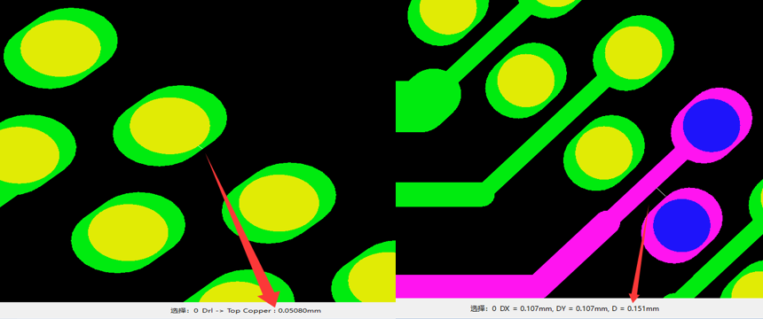
Annular ring: 0.05 mm on certain pads
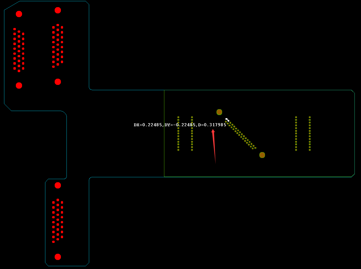
Stiffener: FR4 stiffener with 0.95 mm stiffener hole and 0.31 mm ribs
This combination is common in advanced HDI rigid-flex PCB manufacturing, yet its manufacturability depends heavily on copper behavior, adhesive flow, and drilling tolerances.
Why This Rigid-Flex PCB Was Inherently Difficult?
1. Thick copper increases side-etching risk
With 2 oz copper, the etching rate is higher and lateral etchâoften called side-etchâis harder to control. In this case, the side-etching amount reached: 0.0070 ± 0.003 mm. For ultra-fine traces in a rigid-flex PCB design, this will eat into the design margin.
2. Small annular rings compromise via reliability
Pads with 0.05 mm annular ring severely restrict drilling tolerance. In flex-rigid PCB fabrication, annular rings below 0.10 mm are classified as high-risk features.
3. Extremely tight stiffener clearance
The stiffener needed:
±0.20 mm placement tolerance
±0.05 mm drilling tolerance
But the designer only left 0.15 mm clearance, causing a mismatch between rigid-flex PCB stiffener alignment tolerance and actual manufacturing capability.
4. Thin FR4 stiffener ribs cause glue overflow
Ribs only 0.31 mm wide cannot allow adhesive to retreat during bonding, causing pure glue to overflow and block the stiffener holes.
Technical Challenge #1: Thick Copper Etching with Narrow Spacing
A 2 oz thick copper PCB combined with:
0.15 mm trace/space
0.05 mm annular ring
0.66 mm PTH
creates a situation where compensation is unavoidable.
However, after compensation (~0.007 mm), the remaining trace width would drop to:
0.08 mm (0.15 â 0.07 mm)
This is below the safe manufacturability range of most rigid-flex PCB suppliers.
Best Technology’s solution
Eliminated compensation on 0.15 mm traces
Implemented fine-tuned etching control
Maintained ~0.10 mm final copper width
Ensured full electrical reliability
This is a proven strategy in advanced rigid-flex PCB manufacturing for thick-copper builds.
Technical Challenge #2: Annular Ring Integrity in Plated Through Holes
Annular rings <0.10 mm are extremely vulnerable to:
Drill wander
Etching undershoot
Copper thinning
This is especially critical in high-reliability rigid-flex PCBs, where via integrity is essential.
Best Technology’s solution
Applied rigid-board-level PTH plating process
Improved copper thickness inside the via barrel
Adjusted drilling control to 0.65 ± 0.075 mm
Customer accepted partial ring breakage as long as electrical integrity remained intact
This ensured consistent via performance even in ultra-dense rigid-flex PCB layouts.
Technical Challenge #3: Stiffener Bonding, Alignment, and Adhesive Overflow
1. Why stiffener tolerance was problematic
In rigid-flex PCB assembly, stiffeners are critical for mechanical reinforcement. However:
Hole spacing was only 0.60 mm
Stiffener clearance only 0.15 mm per side
Combined tolerance ±0.25 mm
This inevitably leads to the stiffener covering the pads unless advanced alignment controls are used.
2. Why glue overflow occurs
Thin ribs (0.31 mm) cannot provide an escape path for adhesive. During lamination:
The glue squeezes into the holes
Holes become blocked
Boards fail inspection
3. Best Technologyâs engineered solution
Pre-laminated pure adhesive onto FR4 stiffener
Re-drilled stiffener holes after bonding
Greatly reduced glue overflow
Added 100% AOI + manual inspection for hole clearing
Rejected defective boards, shipped only fully passing units
This is a common best practice in flex PCB stiffener processing when tolerances are tight.
DFM Guidelines for Rigid-Flex PCB Designers
Avoid annular rings under 0.15 mm, especially in 2 oz copper flex-rigid PCB design.
Avoid combining thick copper with fine lines, this will increase manufacturing risk.
Ensure stiffener clearance > total tolerance stack-up. If your clearance is smaller than the alignment tolerance, the stiffener will inevitably shift.
Keep stiffener ribs â„0.5 mm
Send your design for DFM review before finalizing. A goodrigid-flex PCB manufacturer will help adjust the stack-up, drill size, and stiffener layout to avoid expensive redesigns.
This case demonstrates how a complex rigid-flex PCBâwith 2 oz copper, ultra-fine traces, small annular rings, and extreme stiffener constraintsâcan be successfully manufactured through detailed engineering, advanced process control, and disciplined quality screening.
Best Technology combines strong fabrication capability with practical DFM insight, enabling customers to produce compact, reliable, and manufacturable rigid-flex PCB designs that perform consistently under demanding conditions.
If you need support with your next rigid-flex or flex PCB project, our engineering team is ready to assist with stack-up review, DFM checks, or trial builds.
As global electronics manufacturing moves away from hazardous substances, lead free solder material has become the industry standard for PCB assembly. Driven by regulations such as RoHS and REACH, lead-free solder is now used in consumer electronics, automotive PCBs, industrial control boards, and medical devices.
However, not all lead-free solder materials are the same. Their composition, melting temperature, mechanical strength, and reliability vary significantlyâmaking material selection critical for high-quality PCB assembly.
This guide explains what lead-free solder is, its composition, properties, types, melting temperatures, common soldering issues, and finally answers the key question: âWhich lead free solder material is best for PCB assembly?â
What Is Lead Free Solder Material?
Lead free solder material is a metallic alloy used to join components to a PCB without the use of lead. Traditional solder contained 40% lead (Sn60/Pb40) or 37% lead (Sn63/Pb37). These alloys were easy to use but posed environmental and health concerns. Today, electronics manufacturers worldwide use lead-free formulations based on tin, silver, copper, bismuth, nickel, or small alloying elements.
From a customerâs perspective, lead free solder material is important because it directly affects:
Solder joint strength
Heat tolerance
Long-term reliability
Appearance of solder joints
Compatibility with high-density SMT packages
Product compliance with RoHS, REACH, and WEEE regulations
Lead-free solder also withstands higher temperatures, which is critical for modern high-density PCBs.
Is Lead-Free Solder Still Toxic?
Lead-free solder eliminates leadâa major toxic substanceâbut that does not mean every alloy is completely risk-free. For normal PCB manufacturing environments, lead-free solder is considered safe and non-toxic when handled properly.
From a customer standpoint:
Lead-free solder is significantly safer than leaded solder
It does not release toxic lead fumes during reflow
Flux fumesânot the solderâare usually the irritation source
Lead-free waste requires less strict disposal procedures
Most concerns come from misunderstanding. Lead-free alloys like SAC305 (Sn96.5 Ag3.0 Cu0.5) are not harmful under standard handling and reflow conditions. With adequate ventilation and proper gloves, operators face minimal exposure risks.
Lead Free Solder Material Composition
Lead-free solder material compositions vary depending on cost targets, performance needs, and thermal sensitivity of the PCB. Below is a customer-friendly comparison of common alloys:
Common lead-free soldering compositions
Alloy Type
Composition
Characteristics
Best Use
SAC305
Sn96.5 / Ag3.0 / Cu0.5
Most popular global alloy; balanced cost and performance
SMT reflow, general assembly
SAC405
Sn95.5 / Ag4.0 / Cu0.5
Higher silver for stronger joints and better wetting
Automotive, medical, mission-critical devices
SAC0307
Sn99 / Ag0.3 / Cu0.7
Cost-effective low-silver alternative
Consumer electronics, cost-controlled projects
Sn99.3Cu0.7
Tin/copper mix
Slightly higher melting point; durable in wave soldering
Wave solder baths
Sn-Bi alloys
Tin + Bismuth blends
Low melting point; ideal for heat-sensitive substrates
LED boards, flex circuits, thin PCBs
Sn-Ag alloys
Tin + Silver
Good wetting and moderate melting range
Fine-pitch soldering
Ni-doped SAC
SAC + Ni
Improved grain refinement
Automotive, aerospace
For most consumer and industrial applications, SAC305 is the ideal balance of performance and cost. Customers requiring high-temperature reliability (automotive, aerospace, telecom) may consider doped SAC alloys.
Lead Free Solder Material Properties
Lead-free solder is a low-lead soldering material based mainly on tin-based alloys such as Sn-Ag-Cu, Sn-Cu, and Sn-Bi. It is designed to replace traditional Sn-Pb solder and meet environmental regulations such as RoHS while reducing heavy-metal pollution. Itâs properties can be explained from different aspects:
1. Physical & Process Characteristics
Melting Range: Wide, typically 138°Câ250°C depending on alloy. SAC305 melts around 217°C. Most alloys have a narrow solidâliquid range for stable soldering.
Wetting: Good wetting behavior during reflow (30â90 seconds above liquidus) and wave soldering (â4 seconds contact), forming reliable joints.
Conductivity: Electrical conductivity around â„9.5Ă10â¶ S/m and thermal conductivity near 66 W/m·K, similar to Sn-Pb alloys.
Oxidation & Flow: Strong anti-oxidation and smooth flow with low dross generation, reducing defects such as bridging and solder spikes.
2. Mechanical Performance
Strength & Fatigue: Mechanical strength and fatigue life can be optimized through alloy design. Sn-Ag-Cu systems (e.g., 95.4Sn/3.1Ag/1.5Cu) offer strength comparable to or better than Sn-Pb.
Brittleness: Higher Ag or Cu content may reduce ductility, so alloy balance is important.
Reliability: Lead-free joints maintain stability under vibration and thermal cycling, suitable for harsh applications like automotive electronics.
3. Environmental & Cost Characteristics
Compliance: Lead content is typically below 1000 ppm, fully RoHS-compliant and safer for workers and the environment.
Cost: Generally 2â3Ă higher than traditional solder due to tin and silver pricing, but the impact on total product cost is usually limited.
4. Application & Compatibility
Lead-free solder is widely used in consumer electronics, automotive systems, medical devices, and new-energy applications. It works with standard fluxes and existing equipment such as 8-zone reflow ovens, though reflow profiles and process parameters may require adjustment to accommodate higher melting temperatures.
Types of Lead Free Soldering Method
Lead-free soldering involves several manufacturing methods designed around different processes, temperature profiles, and assembly requirements. When customers review PCB assembly quotes, the type of soldering used has a major impact on product durability, electrical integrity, and cost. Below are the core types of lead free soldering used in modern electronics production.
1. Lead-Free Reflow Soldering (SMT Reflow)
This is the most common method for mounting surface-mount components (SMDs). Manufacturers print lead-free solder paste onto pads, place components via pick-and-place machines, and heat the PCB in a controlled reflow oven. Reflow soldering has many advantages:
Suitable for nearly all SMT components
Works with SAC305, SAC405, SAC0307, and Sn-Bi pastes
Ensures consistent joint quality in mass production
235â250°C, depending on the alloy and PCB materials
Reflow soldering is the backbone of every modern SMT line and the main reason SAC305 is widely used.
2. Lead-Free Wave Soldering
Wave soldering is used primarily for through-hole components and mixed-technology assemblies.
During lead-free wave soldering, the PCB passes over a molten solder âwaveâ typically made of Sn99.3Cu0.7 or other tin-rich alloys.
Why customers care:
Ideal for high-volume assemblies with many through-hole connectors
Faster than hand soldering
Strong, uniform joints across large PCBs
But requires strict temperature control due to higher melting points
Common lead-free wave solder alloy
Sn99.3/Cu0.7, with optional micro-alloying (Ni, Ge) to reduce copper dissolution
Typical pot temperature
255â265°C, depending on alloy
3. Lead-Free Selective Soldering
Selective soldering is used when only certain through-hole components must be soldered without exposing the entire PCB to a wave. A programmable nozzle creates localized molten solder âmini waves.â
Why customers care:
Protects heat-sensitive components
Reduces overall thermal stress
Useful for complex PCBs with dense SMT areas
Generates precise and stable joints
Common alloys
Sn99.3Cu0.7
SAC variants for specialized cases
Selective soldering is popular in industrial controllers, automotive electronics, and telecom boards.
4. Lead-Free Hand Soldering
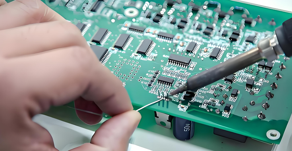
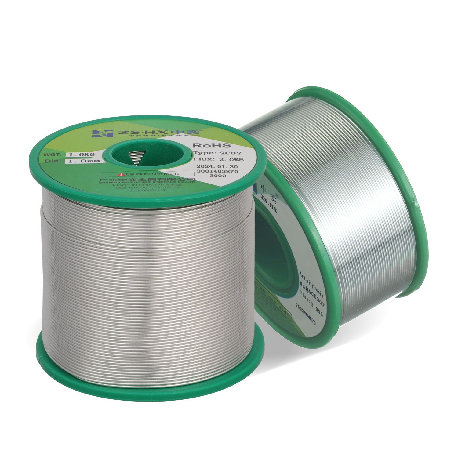
Used for repair, prototyping, or small-batch assembly. Technicians use solder wire (typically SAC305 or SAC0307) and temperature-controlled irons.
Why customers care:
Required for last-minute rework
Used in prototype and engineering samples
Easy way to repair or modify boards
Quality depends heavily on operator skill and iron temperature
Hand soldering temperature
350â380°C for SAC alloys
280â310°C for Sn-Bi low-temp solder
Here is a quick comparison between these lead-free solder material methods:
Soldering Type
Main Features
Typical Alloys
Customer Use Case
Reflow Soldering
Standard SMT process
SAC305, SAC0307
Consumer & industrial electronics
Wave Soldering
High-volume through-hole
Sn99.3Cu0.7
Power boards, large PCBs
Selective Soldering
Localized soldering
Sn-Cu, SAC
Mixed-technology PCBs
Hand Soldering
Rework / prototyping
SAC305 wire
Engineering builds, repairs
Does 60/40 Solder Contain Lead?
Yes, 60/40 solder (Sn60/Pb40) contains 40% lead, so it is not RoHS compliant and must not be used in modern commercial electronics.
Lead-free solder materials replace this alloy entirely in global manufacturing unless exemptions apply (e.g., military or aerospace exceptions).
Lead-Free Solder Melting Temperature Chart
Below is a melting temperature chart customers can use as a reference during material selection or reflow profile planning:
Lead-Free Alloy
Melting Temperature (°C)
Notes
SAC305
217â220°C
Most common for SMT
SAC405
217â225°C
Higher Ag content improves strength
SAC0307
~227°C
Budget option; slightly higher melting point
Sn99.3Cu0.7
227°C
Ideal for wave soldering
Sn-Bi
138â170°C
Best for low-temp applications
Sn63/Pb37 (leaded)
183°C
For comparison only
Customers should always verify that their components can tolerate the peak reflow temperature required by the alloy.
What Are the Main Issues With Lead-Free Soldering?
Lead-free soldering is reliable, but it requires proper process control. Common challenges include:
Higher melting point that stresses components
Slower wetting that demands optimized flux
Sometimes duller appearance of joints
Increased copper dissolution in wave soldering
Sensitivity to reflow temperature deviations
Why Is My Lead-Free Solder Not Melting?
Typical causes include:
Iron or reflow temperature not high enough.
Insufficient heat transfer due to oxidation or contamination.
Using a low-power soldering iron unable to maintain temperature.
Weak flux activity preventing proper heat flow.
Applying the solder to a large thermal pad without preheating.
Lead-free solder requires around 30â40°C higher heat than leaded solder.
Which Lead Free Solder Material Is Best for PCB Assembly?
For most customers, SAC305 (Sn96.5/Ag3.0/Cu0.5) is the best lead-free solder material for PCB assembly.
Why SAC305 Is Ideal for Most Applications?
Widely used across global SMT factories
Excellent wetting on FR4, HDI, flexible, and ceramic substrates
Strong mechanical performance
Good thermal cycling reliability
Low voiding rate with proper reflow control
Compatible with nearly all flux chemistries
Proven in millions of consumer and industrial electronics
When Other Alloys Might Be Better?
SAC0307 â When cost is the priority
Sn-Bi â For low-temperature PCBs and LED products
SAC405 â For high-reliability automotive or medical electronics
Sn99.3Cu0.7 â For wave soldering to reduce cost
Customer Recommendation
If you are unsure which alloy to choose, start with SAC305 for standard SMT reflow because it aligns with:
Reliability expectations
Cost targets
Compatibility with modern assembly lines
Strong field performance
FAQs
1. What is the most common lead-free solder in SMT assembly?
SAC305 is the industry standard for most SMT production lines.
2. Is lead-free solder as strong as leaded solder?
Yes. Lead-free joints are typically stronger in mechanical strength and thermal fatigue resistance.
3. Why is lead-free solder harder to work with manually?
It melts at a higher temperature and wets more slowly, requiring better temperature control.
4. What flux should be used with lead-free solder?
Most solder pastes use no-clean or water-soluble fluxes optimized for SAC alloys.
5. Can lead-free solder be used with ENIG finish?
Yes, ENIG is one of the best surface finishes for consistent wetting.
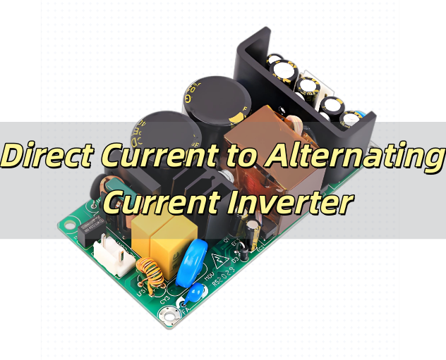
What Is Direct Current to Alternating Current Inverter?
A direct current to alternating current inverter is a sophisticated electronic device that transforms the stable, unidirectional flow of direct current (DC) into the oscillating waveform of alternating current (AC). Since most household appliances, industrial equipment, communication devices, and commercial systems are designed to operate on AC power, an inverter becomes essential whenever the primary energy source produces DCâsuch as a battery bank, solar photovoltaic array, fuel cell system, or automotive electrical system.
A direct current to alternating current inverter not only changes the type of current but may also adjust voltage levels, regulate frequency, stabilize output under varying load conditions, and provide protection against overload, short circuits, and reverse polarity. Modern inverters are used in renewable energy systems, emergency backup installations, portable power stations, RVs, boats, telecom sites, medical support equipment, and mobile power environments where AC power is required but unavailable.
Types of DC-AC Inverters
DC-AC inverters differ significantly in waveform purity, output stability, conversion efficiency, and suitability for specific applications. The main categories include:
1. Pure Sine Wave Inverters
These inverters generate an AC waveform that closely replicates grid-quality electricity. The output features smooth, continuous voltage oscillation with minimal harmonic distortion, making it compatible with all AC-powered devices. Sensitive electronicsâsuch as medical monitors, refrigeration compressors, audio devices, laser printers, and precision measurement instrumentsâoperate best on pure sine wave power. These inverters typically offer high efficiency, low noise, and stable operation under both linear and non-linear loads.
2. Modified Sine Wave Inverters
A modified sine wave inverter uses a stepped waveform that approximates AC power. Although not as clean as pure sine wave output, this type performs adequately for many non-sensitive devices, including power tools, lighting equipment, small appliances, and general-purpose electronics. Modified sine wave inverters are more cost-effective but may cause increased heat, lower efficiency in some motors, or buzzing noise in audio equipment.
3. Square Wave Inverters
Once common in small or low-cost electrical systems, square wave inverters produce a simple on/off AC waveform. This waveform is harsh for most modern electronics and is primarily compatible with resistive loads like heaters or incandescent bulbs. Because of poor performance with inductive and capacitive loads, square wave inverters are rarely used in contemporary systems.
4. Hybrid Inverters
Hybrid inverters integrate battery charging, solar input control, grid synchronization, and energy management in a single platform. These inverters can automatically switch between solar energy, battery storage, and utility grid power, optimizing system efficiency. Hybrid inverters are the backbone of modern off-grid and grid-tied solar systems, providing seamless power transition during outages and offering advanced monitoring functions.
How Does a DC-AC Inverter Work?
A DC-AC inverter performs conversion through multiple coordinated electrical stages, each responsible for shaping and regulating the characteristics of AC output.
1. Input Filtering and Conditioning
The inverter receives DC power from a battery or solar module. Input filters remove noise and voltage spikes that may cause output instability.
2. High-Frequency Switching Stage
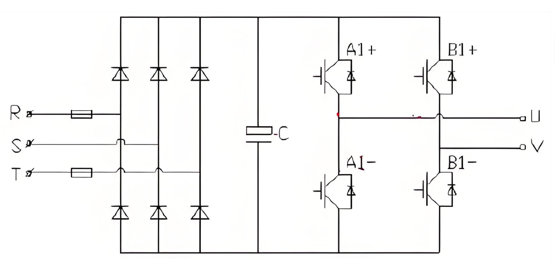
At the core of the conversion process are semiconductor switches (MOSFETs or IGBTs). These switches operate at high frequencyâoften tens of kilohertzâto chop the DC into rapid pulses. The switching frequency and modulation pattern determine the waveform shape and voltage regulation.
3. Pulse-Width Modulation (PWM)
PWM is used to control the effective voltage delivered to the load. By adjusting the width of each pulse in the switching pattern, the inverter can simulate the smooth rise and fall of AC voltage.
4. Step-Up or Step-Down Conversion
Some inverters use transformers or boost converters to raise or lower DC voltage before waveform synthesis. This allows 12V, 24V, or 48V DC inputs to generate 120V or 230V AC output.
5. Waveform Smoothing and Filtering
Inductors and capacitors smooth the PWM output, reducing harmonic content and producing a stable AC sine wave.
6. Output Regulation and Protection
Advanced inverters constantly monitor output voltage, frequency, temperature, load level, and internal current flow. Protection features prevent damage from overload, overheating, short circuits, polarity reversal, or low input voltage.
DC to AC Conversion Formula
The dc to ac conversion formula is essential for determining how much usable AC power an inverter can produce from a DC source:
AC Output Power = DC Input Power Ă Inverter Efficiency
Where: DC Input Power = DC Voltage Ă DC Current Inverter efficiency typically ranges from 85% to 96%.
To estimate how much AC load an inverter can safely support, users should consider cable loss, temperature effects, continuous versus surge power, and battery voltage drop under load. For converting DC voltage levels into AC voltage, inverters use a combination of high-frequency switching and transformer-based or transformerless boost stages.
How to Convert DC to AC without Inverter?
Although not recommended for most modern applications, DC can be converted to AC without a conventional inverter through alternative methods.
1. Motor-Generator System
A DC motor mechanically drives an AC generator. As the generator rotates, it produces an alternating voltage waveform. This method is robust but extremely inefficient, noisy, and heavy, making it unsuitable for portable or energy-sensitive environments.
2. Rotary Converters
Rotary converters were historically used in railways and heavy industry to convert DC to AC. They consist of rotating machinery and commutators that mechanically modulate current. Today they are rarely used due to high maintenance requirements and poor energy efficiency.
3. Electronic Oscillator + Transformer Method
A custom-built oscillator circuit can generate AC-like waveforms, which are then amplified and stepped up through a transformer. While feasible in theory, this method requires advanced electronics knowledge and cannot match the stability or safety of a commercial inverter.
All alternative methods produce unstable or noisy AC output, reinforcing that a modern inverter remains the safest and most reliable solution.
DC Current to AC Current Calculator
A dc current to ac current calculator helps users determine the AC current available after conversion losses. The calculation is:
AC Current = (DC Voltage Ă DC Current Ă Efficiency) Ă· AC Voltage
Example:
DC voltage: 12V
DC current: 50A
Efficiency: 90%
AC output voltage: 120V
AC Current = (12 Ă 50 Ă 0.9) Ă· 120 = 4.5A AC
Key considerations include battery voltage level, load characteristics, wire length, and conductor size. Low battery voltage reduces AC output, and long cable runs may cause voltage drops. This calculation is widely used in solar power engineering, RV system design, and battery-power planning.
Applications of DC-AC Inverters
DC-AC inverters are indispensable across a wide range of industries and environments. By enabling DC sources to run AC loads, they open up deployment possibilities for many types of power systems.
Solar PV systems converting sunlight into usable home or commercial AC power
RVs, campers, and vans powering home-style appliances on the road
Marine systems supporting onboard AC circuits on yachts and boats
Industrial field tools used in remote or temporary work sites
Emergency and backup systems providing reliable power during grid failure
Portable power stations used in camping, travel, or disaster relief
Telecom towers powering AC-based equipment in remote locations
Medical support devices requiring stable AC power from mobile batteries
The ability to transform DC energy into AC makes inverters one of the most versatile electrical devices in modern power systems.
Safety Guidelines for Using a DC-AC Inverter
Proper installation ensures reliability, safety, and long operational life. Following good engineering practice reduces risk and prevents avoidable failures.
Use appropriate cable gauge to prevent overheating and voltage drop.
Maintain reliable grounding to minimize shock hazards and noise issues.
Ensure ventilation so that heat can dissipate and components stay within safe temperature.
Avoid overloading by keeping AC load within rated continuous and surge capacities.
Install circuit breakers and fuses in both DC input and AC output as required for system protection.
Keep inverter away from moisture and dust to prevent corrosion and tracking.
Check connection tightness regularly to avoid arcing and unwanted resistance.
Monitor battery condition because weak or damaged batteries can cause unstable operation.
How to Test a DC-AC Inverter?
Thorough testing evaluates the health, efficiency, and reliability of the inverter. A structured test process helps identify potential issues before they lead to downtime.
1. DC Input Voltage Check
Verify that the battery or DC source is supplying stable voltage. Under-voltage conditions may trigger protective shutdown, while over-voltage can damage components.
2. AC Output Voltage Measurement
Use a digital multimeter to confirm that the inverter is producing the correct AC voltage according to its rating (such as 110V, 120V, or 230V).
3. Load Test
Connect a resistive load or a group of appliances with known power ratings. Observe whether the inverter maintains consistent voltage and frequency under load without overheating or shutting down.
4. Waveform Quality Inspection
An oscilloscope can reveal waveform type, distortion, spikes, and harmonic content. This is particularly important when powering sensitive electronics or motors.
5. Temperature Monitoring
During extended operation, monitor the inverter casing and internal components for excessive heat. High temperature can indicate insufficient ventilation or overloading.
6. Safety Feature Validation
Test overload protection, low-voltage shutdown, over-temperature shutdown, and short-circuit response. Confirm that the inverter behaves safely during fault conditions.
Why Do DC-AC Inverters Fail? Common Problems
Inverters may fail due to a variety of electrical, mechanical, and environmental factors. Understanding these reasons helps designers and users prevent downtime.
Overloading that pushes components beyond their power and thermal limits.
Poor ventilation leading to heat buildup and thermal stress on semiconductors.
Low-quality components that degrade faster under high-frequency switching.
Incorrect wiring causing hot spots, arcing, or repeated fuse failures.
Battery instability with large voltage swings affecting DC input.
Moisture and dust causing corrosion, short circuits, or insulation breakdown.
Harmonic distortion and noise stressing internal power stages over long periods.
Routine inspections, correct system sizing, proper cooling, and adherence to installation guidelines significantly reduce the risk of inverter failure and extend service life.
FAQs
1. What size inverter should I choose? Choose an inverter with a continuous rating 20â30% higher than your total load, and ensure the surge rating can handle motor or compressor startup currents.
2. Are pure sine wave inverters worth the investment? Yes. They provide grid-quality output, protect sensitive electronics, reduce noise, and improve motor efficiency and lifespan compared with modified or square wave inverters.
3. Can an inverter run from a car or RV battery? Yes, but verify that the battery has sufficient capacity and that cables are correctly sized. Avoid draining the battery below recommended voltage levels to preserve battery health.
4. Do inverters waste energy? Inverters lose approximately 5â12% of energy as heat. High-efficiency models reduce this loss and are preferable in solar and off-grid systems where every watt counts.
5. How long can an inverter operate continuously? A high-quality inverter can run continuously as long as it has proper ventilation, a stable DC supply, and operates within its rated load and temperature limits.
6. Can solar panels connect directly to an inverter? Most systems require a solar charge controller and battery buffer to manage voltage and protect both panels and inverter. Only specialized inverters are designed to accept direct PV input.
7. How often should an inverter be inspected or tested? For general use, inspection every few months is recommended. Off-grid, telecom, medical, or mission-critical systems may require more frequent testing and monitoring.
The system board is one of the core elements inside every modern electronic device. Whether you use a laptop, desktop PC, tablet, medical device, industrial controller, or even consumer IoT equipment, everything begins with the system board. It is the foundational circuit structure that connects, coordinates, and powers all major hardware components. Without it, a device cannot turn on, cannot transfer data, and cannot function reliably.
Many people know this component by another familiar name: the motherboard. In most contexts, both terms refer to the same thing. However, when you evaluate technical documentation, service manuals, OEM repair guides, or industrial product sheets, you will often encounter the phrase âsystem boardâ because it reflects a more functional description of the boardâs role. This guide will explain what the system board is, why it matters, what components it contains, and how to differentiate system board vs motherboard.
What Is the System Board?
What Is the System Board? System Board Definition
A system board is the main printed circuit board that hosts and interconnects all major hardware components of an electronic device. It distributes power, manages data communication, holds connectors, supports the CPU and memory, and integrates the firmware that controls boot and hardware configuration.
In a practical sense, the system board is the central nervous system of any computer or smart device. All processing, storage, communication, and peripheral interaction begin with it.
Key characteristics of a system board include:
It houses the CPU or SoC
It provides slots and interfaces for memory, storage, and expansion devices
It manages internal and external I/O
It contains the chipset or controller hub that coordinates system communication
It provides power regulation for critical components
It holds firmware such as BIOS or UEFI
This definition applies across device types, from high-performance servers to compact embedded systems.
Types of System Boards
Because electronic products vary greatly in size, function, and performance demands, system boards come in multiple categories.
1. Desktop System Boards
Common form factors: ATX, Micro-ATX, Mini-ITX. These boards offer replaceable components, expansion slots, GPU support, and thermal flexibility.
2. Laptop System Boards
Compact and heavily optimized. Many components, like RAM or CPU, may be soldered to save space.
3. Server System Boards
Engineered for reliability and scalability. Typical features: multi-CPU sockets, ECC memory support, redundant power design, strong I/O capacity.
4. Embedded and Industrial System Boards
Used in factories, automation equipment, medical devices, and IoT controllers. Highly customizable layouts and long lifecycle availability.
5. Mobile Device System Boards
Found in smartphones and tablets. Use integrated SoC packages with wireless modules, power regulators, and dense multilayer stack-ups.
Each type has a different design approach, but they all perform the same core role: providing the platform on which the entire system operates.
How Does a System Board Work?
A system board works by acting as the central communication and power distribution platform for all hardware inside a device. Every major componentâCPU, memory, storage, graphics, power modules, and external interfacesârelies on the system board to operate in sync. It functions as both the electrical backbone and the coordination center of the entire system.
It is the one component that must function perfectly for the entire system to operate. At every moment, the system board is directing traffic among dozens of active hardware elements.
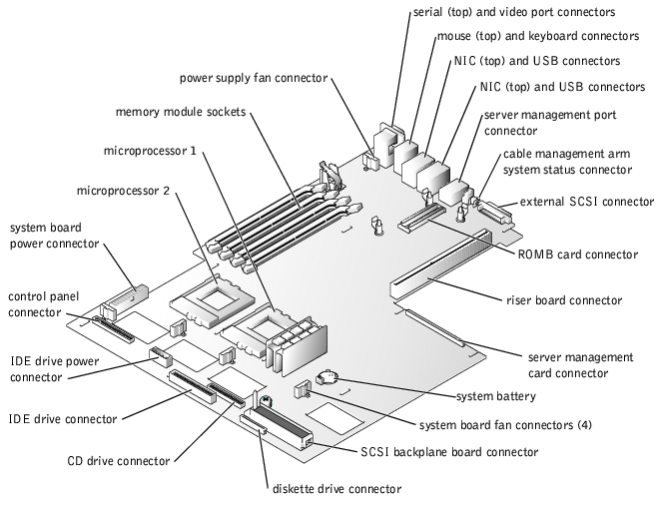
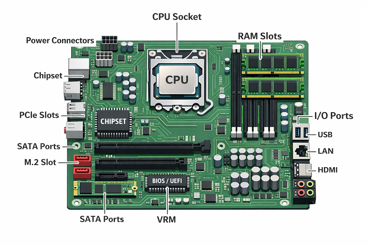
System Board Diagram
Below is a simplified conceptual layout of a typical system board, it includes:
CPU socket
Chipset (Northbridge/Southbridge or PCH)
Memory (DIMM/SODIMM slots)
PCIe slots
Storage interfaces (M.2, SATA)
Power connectors (24-pin, 8-pin CPU)
I/O interfaces (USB, Ethernet, audio)
BIOS/UEFI firmware chip
VRM power modules
Internal headers (fan, front panel, RGB, etc.)
This diagram helps visualize how tightly integrated the components are and how the board organizes both power and data pathways.
What Is the Purpose of the System Board?
The core purpose of the system board is to:
Integrate all essential components into a unified platform
Enable communication between hardware modules
Provide physical mounting points and electrical pathways
Supply and regulate power from the power input
Facilitate system startup and firmware control
Handle data flow to internal and external devices
Put simply, it is the foundation on which the entire computing system is built.
Key Components Found on a System Board
A modern system board integrates a wide range of functional components:
Each element contributes to the total functionality and performance capability of the device.
System Board vs Motherboard: What Are the Differences?
Although many people treat these terms as identical, there are subtle distinctions:
System Board
Used in enterprise service documents
Emphasizes system-level integration
Common in servers, industrial controllers, embedded systems
More neutral, technical terminology
Motherboard
Popular in consumer PC building
More common in desktop, gaming, and DIY markets
Focuses on expandability and performance features
Broadly recognized by non-technical users
Key takeaway
Both terms describe the same type of hardware, but they differ in usage context.
What Is the System Board Used For?
Anywhere data is processed or controlled, a system board exists. System boards are found in nearly all electronic systems:
Desktop PCs
Laptops
Smartphones
Servers
Medical devices
Automotive electronics
Industrial automation controllers
Robotics
Consumer electronics
IoT devices
Network equipment
Why System Board Manufacturing Requires Professional PCB & PCBA Capabilities?
Although readers usually think of the system board as a finished computer component, its reliability begins much earlier in the PCB manufacturing and assembly stages. A system board is a complex, multilayer PCB with dense routing, high-speed interfaces, strict impedance control, and tight thermal requirements. This makes the quality of its PCB and PCBA processes critical.
Modern system boards typically include:
Multilayer stack-ups (8L, 10L, 12L and above)
High-speed differential pairs for PCIe, USB, HDMI, LVDS
Controlled impedance traces for stable signal integrity
BGA and LGA CPU packages
Fine-pitch connectors and ultra-dense component layouts
High-current VRM power stages
M.2, SATA, and PCIe slot soldering
Embedded controllers, BIOS/UEFI ICs, and power management circuits
Manufacturing and assembling such boards requires precision, stability, engineering support, and strict testing procedures.
This is exactly where EBest Circuit (Best Technology) helps global customers gain reliable performance.
How EBest Circuit (Best Technology) Supports System Board Production?
EBest Circuit (Best Technology) has long served customers who require complex mainboards, server logic boards, laptop controller boards, industrial control boards, and embedded system boards. Our fabrication and assembly services are engineered to meet the stringent requirements of system-level products.
For system boards, precise soldering of BGA CPU sockets, M.2 connectors, PCIe slots, and high-speed controllers is essentialâand our inspection workflow ensures stable solder quality.
System boards must pass strict testing because they are the âbrainâ of the entire device.
We use:
Flying-probe testing
Automated in-circuit testing (ICT)
Functional testing based on customer firmware
Boundary scan (JTAG) for high-density digital boards
Burn-in testing upon request
High-layer count PCBs often hide defects deep inside the stackup, so our process ensures that every board delivered meets performance expectations.
4. Full Engineering Support
Stack-up design assistance
DFM / DFA review
Impedance simulation
Material recommendation for high-speed designs
Prototype revision feedback
One-stop BOM sourcing
Our engineering team collaborates directly with OEMs, industrial designers, and hardware architects to optimize manufacturability before production begins.
Why Many Global Brands Choose EBest Circuit (Best Technology) for System Board Projects?
Companies choose EBest Circuit (Best Technology) because we provide:
One-stop PCB + PCBA integration
Factories in China and Vietnam for flexible cost and lead time
High-layer, high-speed, HDI capability for complex logic boards
Professional SMT assembly with strict inspection
On-time delivery and stable quality
UL, ISO 9001, ISO 13485, AS9100D and IATF 16949 quality certifications
Over a decade of experience serving electronics, industrial, automotive, medical, and computing customers
If you are developing a system board, embedded controller, logic board, medical equipment mainboard, or industrial computer board, EBest Circuit (Best Technology) can support you from prototype to mass production.
To get a fast quotation or technical consultation:
We will evaluate your Gerber files, BOM, and assembly requirements, then provide optimized PCB stack-ups, material choices, and lead-time proposals based on your project needs.
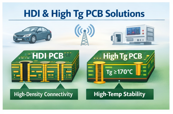
Why do HDI & high TG PCB solutions matter so much for high-reliability electronics? Because failures rarely come from a single âbigâ mistake. They often start from small issues: marginal solder joints, microcracks around vias, drift in impedance, or repeated thermal shock.
An HDI PCB helps by shortening trace length, controlling impedance, and reducing stubs. A high Tg PCB helps by raising the glass transition temperature, so the board structure stays stable under higher reflow and operating temperatures.
When you integrate both, you gain:
Better control of high-speed signals in dense layouts
Stronger resistance to repeated lead-free reflow cycles
Improved reliability in wide temperature ranges
Smaller, lighter boards that still carry complex circuits
For sectors like automotive ADAS, 5G equipment, and industry automation, this combination is often no longer ânice to haveâ. It becomes a base requirement.
What Are HDI & High Tg PCB Solutions?
HDI & High Tg PCB solutions refer to PCB designs that use high-density interconnection structures together with high-temperature glass transition materials. Rather than treating HDI PCB and high Tg PCB as separate topics, this concept views them as a design âtoolboxâ that works as a system.
A typical HDI & high Tg PCB stack-up may include:
High Tg FR4 or hybrid material core
One or more HDI buildup layers with microvias
Fine lines and spaces for dense routing
Controlled impedance structures for high-speed signals
Multiple lamination cycles using high Tg prepregs
These solutions focus on two goals at the same time: interconnection density and temperature endurance. The design approach covers layout rules, via strategy, material selection, and process limits from the start, not as late-stage fixes.
What Is an HDI PCB and Why Is It Used in Modern Electronics?
Sequential build-up (1+N+1, 2+N+2, 3+N+3, and so on)
Fine line/space (e.g., 75 ”m/75 ”m or better)
Via-in-pad for BGA breakout
Modern ICs such as high pin-count BGAs, fine-pitch QFNs, and SiP modules simply cannot be routed on old-style 1-via-per-pin layouts. HDI PCB structures shorten critical paths, reduce via stubs, and keep return paths tight.
Key advantages of hdi pcb in modern designs include:
Smaller board size with the same or higher function density
Better signal integrity for multi-gigabit links
Improved power distribution with dense stitching vias
Room for mechanical design freedom in slim devices
Because of this, HDI PCB technology is common in smartphones, tablets, communication modules, automotive radar, and compact industrial controllers.
What Is a High Tg PCB and How Does It Improve Reliability?
A high tg pcb uses laminate with a higher glass transition temperature than standard FR4. Tg is the point where the resin system changes from glassy to rubbery. Above this point, mechanical properties weaken quickly.
In a high Tg PCB, the Tg value might be 170â180°C or higher, instead of around 130â140°C for common materials. This increased Tg gives several benefits:
Better dimensional stability during lead-free reflow
Lower risk of pad lifting, delamination, or barrel cracks
Reduced mechanical stress during temperature cycling
Improved long-term reliability in high-temperature service
High Tg PCB materials also tend to have better thermal endurance over time, which helps in automotive under-hood zones, power supplies, motor drives, and LED lighting. They can handle more thermal stress without visible or hidden damage.
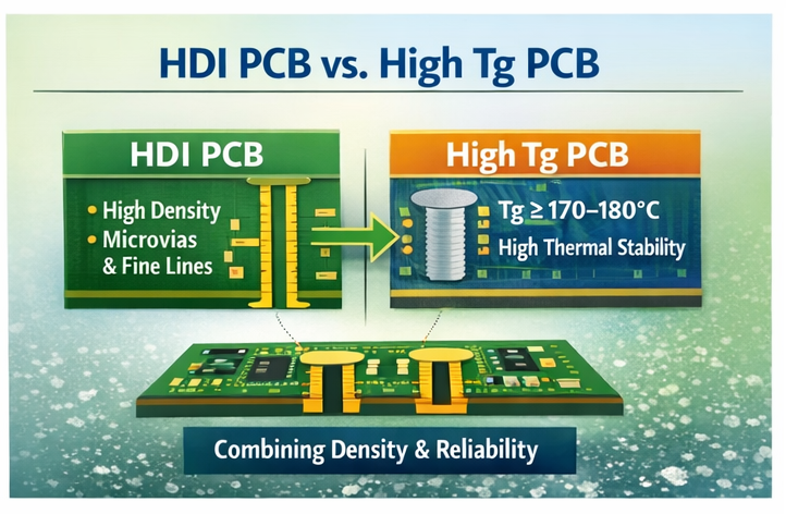
Differences Between HDI PCB and High Tg PCB
HDI and high Tg describe two different aspects of a PCB: one structural, one material. They often coexist, but they are not the same.
Aspect
HDI PCB
High Tg PCB
Main focus
Interconnect density and routing
Thermal and mechanical stability
Key features
Microvias, fine lines, via-in-pad
Tg â„ 170â180°C, better thermal endurance
Typical driver
Fine-pitch BGAs, compact form factor
Lead-free reflow, high operating temperature
Impact on layout
Strong effect on routing and stack-up
Moderate; affects stack-up and DFM margin
Impact on reliability
Better signal and via performance
Lower risk of warpage and delamination
Cost drivers
Laser drilling, lamination cycles, yield
Material price, process window, lamination setup
An HDI PCB can use standard Tg material when the thermal profile is mild. A high Tg PCB can have no HDI features at all if density remains low. When the project pushes both limits, you combine them.
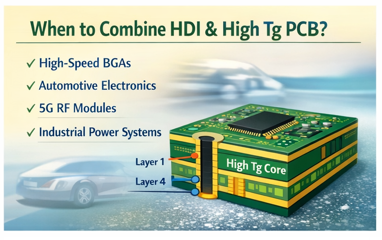
When Should HDI PCB and High Tg PCB Be Combined?
Combining HDI PCB and high Tg PCB makes sense when a design faces both density and thermal stress at the same time. Typical cases include:
High-speed compute boards with large BGAs and multiple reflow passes
Automotive radar or camera modules near engines or outdoor zones
5G RF front-ends in compact housings with limited airflow
Industrial motion control or power electronics running at elevated temperature
You should consider an HDI & high Tg PCB solution if:
The layout requires microvias or sequential lamination to escape key components
The assembly line uses lead-free profiles with high peak temperature
The product will see frequent on-off cycling or wide ambient temperature swings
Field reliability and long service life carry high business value
In these scenarios, HDI brings routing freedom and signal quality, while high Tg materials protect the board structure against thermal and mechanical stress.
Medical devices: Imaging equipment, patient monitoring, compact diagnostic tools
Consumer and wearable devices: Smartphones, tablets, smartwatches, AR/VR devices
All these products share common requirements: compact size, strict reliability targets, and long-term stability under shifting loads. HDI PCB structures handle fine-pitch and high-speed paths, while high Tg PCB materials carry the thermal and mechanical burden.
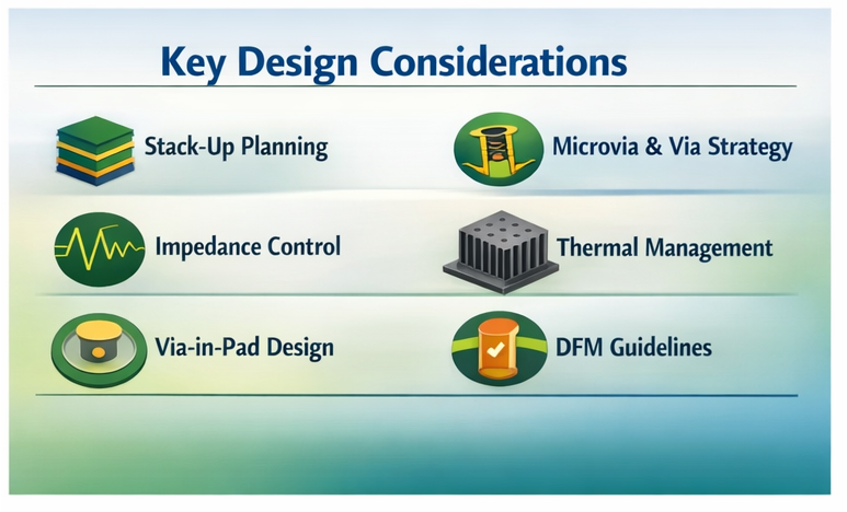
What Are the Key Design Considerations for HDI & High Tg PCB?
Designing HDI & high Tg PCB solutions is not just about choosing a material with higher Tg and shrinking traces. It needs careful coordination between layout, stack-up, and process limits. Key points include:
1. Stack-up planning early
Decide the HDI level (1+N+1, 2+N+2, etc.), copper thickness, and layer count early. Include high Tg material data, Dk/Df values, and lamination constraints in the first draft.
2. Microvia and buried via strategy
Keep microvia aspect ratios within the fabricatorâs safe range. Use staggered rather than stacked microvias when reliability priority is high, unless the project can support enhanced filling processes.
3. Impedance control with high-speed pairs
High-density routing often pushes traces close together. Work with the fabricator to set precise trace width and spacing for each impedance class, considering the actual dielectric constant of the high Tg material.
4. Thermal management and copper balance
High Tg PCB materials support higher temperature, but heat still needs paths. Balance copper areas across the panel to reduce warpage. Provide solid ground planes, thermal vias, and clear heat paths.
5. Solder mask and via-in-pad design
When using via-in-pad on HDI pads, confirm filling and capping processes. Poorly filled vias can trap flux or reduce solder joint strength.
6. Design for manufacturability (DFM)
Follow the manufacturerâs design rules for minimum line/space, annular ring, drill size, and pad shapes. Good DFM work reduces scrap and supports stable quality.
What Manufacturing Challenges Exist in HDI & High Tg PCB?
Manufacturing HDI PCB involves several engineering challenges because the process pushes the limits of micro-fabrication, interlayer reliability, material control, and inspection accuracy. Each stage demands strict tolerance management to keep performance stable in high-density layouts.
Microvia and blind-via drilling accuracy is difficult because HDI requires via diameters
below 0.15 mm. Laser drilling must stay stable and precise to avoid rough walls, incomplete holes, or weak plating that may cause electrical issues in stacked via structures.
Layer-to-layer registration and lamination control demand micron-level alignment.
High-order HDI needs multiple lamination cycles, and any shift in imaging, resin flow, or pressure can create opens, shorts, or signal loss.
Fine-line etching becomes harder as line width and spacing drop to 3 mil or less. Thin
traces are sensitive to under-etching or over-etching, and thicker copper (4â10 oz) makes precise control even more challenging.
Plating and via filling must deliver uniform copper to keep interconnections stable.
Voids, trapped gas, or uneven filling weaken microvias and reduce long-term reliability, especially when the design needs high breakdown voltage.
How EBest Circuit (Best Technology) Supports HDI & High Tg PCB Solutions?
EBest Circuit (Best Technology) supports HDI & High Tg PCB Solutions from early design review through mass production and assembly. Our team focuses on turning demanding ideas into stable, repeatable products.
Engineering and DFM for HDI and high Tg
Our engineers review your stack-up, HDI level, and component layout at the start. We suggest suitable high Tg materials, via strategies, and impedance structures based on your performance and cost targets.
HDI PCB manufacturing capability
We support fine line and space routing, laser-drilled microvias, via-in-pad, and multi-step lamination. Typical HDI builds such as 1+N+1, 2+N+2, and higher structures can be handled with controlled registration and repeatable yields.
High Tg and advanced materials
We work with well-known high Tg PCB laminates and can also support hybrid builds for projects that need both RF and digital performance. Material selection focuses on Tg, Td, Dk/Df, and reliability under your real reflow profile.
PCBA assembly with process control
EBest Circuit (Best Technology) provides SMT and through-hole assembly for HDI and high Tg boards in both China and Vietnam. Lead-free profiles, X-ray for BGA, and AOI help keep quality stable for dense layouts.
Quality systems and traceability
Our factories follow ISO9001, ISO13485 for medical, IATF16949 for automotive, and AS9100D for aerospace. We also run MES systems to track each lot from material incoming through final shipment. This supports clear traceability and faster root-cause analysis if any issue appears.
For buyers who need a long-term partner for HDI & high Tg PCB solutions, this combination of engineering support, HDI process capability, and certified quality systems reduces risk and saves internal effort.
FAQs about HDI & High Tg PCB Solutions
1. Is HDI PCB always more expensive than a standard multilayer board?
HDI PCB usually costs more per panel due to laser drilling, extra lamination, and tighter controls. However, the total product cost can drop because the board is smaller, the BOM can be simplified, and performance improves.
2. When do I really need a high Tg PCB instead of normal FR4?
You should consider a high Tg PCB when your design uses lead-free solder, has more than one reflow cycle, or runs in high ambient temperatures. Automotive, power, and industrial products are common cases where high Tg material significantly improves reliability.
3. Can I use HDI without high Tg material for consumer products?
Yes. Many consumer devices use hdi pcb structures on mid-range Tg materials because their operating temperature is moderate and lifetime targets are shorter. The decision depends on your thermal profile and reliability goals.
4. Are stacked microvias less reliable than staggered ones?
Stacked microvias can be reliable when the process is well controlled, but they need stricter plating and filling quality. For very harsh environments, many designers still prefer staggered microvias for extra margin, unless dense routing forces stacking.
5. How early should I involve EBest Circuit (Best Technology) in an HDI & high Tg PCB project?
The best time is before you freeze the stack-up and routing strategy. Early DFM and material discussion help avoid later redesign, reduce risk, and shorten the path from prototype to stable mass production.
If you are planning a new design that needs smaller size, higher speed, and stronger thermal performance, HDI & High Tg PCB Solutions may be the right direction. You can share your Gerber files, stack-up ideas, or even just a concept, and EBest Circuit (Best Technology) will help you evaluate practical options, costs, and timelines for your next project.
This certification confirms that PCB processes are controlled, repeatable, and audited for defect prevention rather than post-inspection.
For automotive buyers, choosing an IATF 16949 certified PCB supplier directly reduces recall risk, audit pressure, and long-term field failures.
What Is an IATF 16949 Certified PCB Supplier?
AnIATF 16949 certified PCB supplier is a PCB manufacturer that complies with the global automotive quality management standard issued by the International Automotive Task Force.
This standard requires:
Full process traceability
Preventive quality planning (APQP, FMEA)
Continuous improvement and corrective action systems
Controlled production from prototype to mass volume
Unlike general certifications, IATF 16949 applies only to automotive supply chains.
What Is an IATF 16949 Certified PCB Supplier?
Why Do Automotive OEMs Require IATF 16949 PCB Suppliers?
Automotive OEMs require IATF 16949 because PCB failures can trigger recalls, safety risks, and regulatory penalties.
This certification ensures:
Stable PCB manufacturing processes
Early risk identification
Consistent quality across production lots
Audit-ready documentation for OEM and Tier-1 reviews
For safety-critical electronics, uncertified suppliers introduce unacceptable risk.
Which Automotive PCBs Must Come from an IATF 16949 Certified Factory?
Automotive PCBs that typically require IATF 16949 certification include:
Engine control units (ECU)
ADAS and camera modules
Radar and RF automotive PCBs
Battery management systems (BMS)
Power inverter and motor control boards
Safety and braking control electronics
If a PCB affects vehicle safety, emissions, or power control, certification is expected.
IATF 16949 vs ISO 9001 for PCB Manufacturing
ISO 9001 focuses on general quality procedures across industries. IATF 16949 focuses on automotive risk prevention and process stability.
Key differences for PCB buyers:
IATF 16949 requires FMEA and PPAP
ISO 9001 allows broader process variation
IATF 16949 enforces corrective action with data
ISO 9001 emphasizes documentation, not automotive reliability
ISO 9001 alone is not sufficient for automotive PCBs.
Core Capabilities Required from an IATF 16949 PCB Supplier
An automotive-qualified PCB supplier must demonstrate both engineering and process discipline.
This includes impedance-controlled stackups, material consistency, SPC monitoring, and documented change control.
Below is a technical capability table automotive buyers often request.
Capability Category
Automotive PCB Requirement
Typical Specification Range
PCB Layer Count
Multilayer & HDI
2â20 layers
Controlled Impedance
Mandatory for high-speed / RF
±5% to ±10%
Copper Thickness
Power and signal balance
0.5â6 oz
Minimum Trace / Space
Dense automotive layouts
3/3 mil
Via Technology
Reliability under vibration
Through, blind, buried, microvia
Laminate Materials
Thermal and electrical stability
High-Tg FR-4, Rogers, hybrid stackups
Surface Finish
Automotive solderability
ENIG, ENEPIG, OSP
Operating Temperature
Harsh environment tolerance
â40°C to +125°C
Traceability System
Mandatory under IATF 16949
Lot-level MES tracking
Quality Documentation
OEM audit compliance
PPAP, FMEA, Control Plan, SPC
Production Volume
Prototype to mass production
NPI â high volume
Reliability Testing
Automotive qualification
Thermal cycling, cross-section
How Traceability Works in IATF 16949 PCB Manufacturing?
In IATF 16949 certified PCB manufacturing, traceability links each PCB lot to materials, processes, inspections, and operators.
Traceability systems typically record:
Laminate batch numbers
Inner layer imaging data
Lamination cycles
Plating and surface finish parameters
Final inspection results
This allows fast containment if field issues occur.
What Quality Risks Exist Without an IATF 16949 PCB Supplier?
Choosing a non-certified PCB supplier increases:
Process variation
Incomplete documentation
Poor root-cause analysis
Audit failures during OEM reviews
These risks often surface only after volume production begins.
What Documents Should an IATF 16949 PCB Supplier Provide?
Automotive buyers should expect:
PPAP documentation
PFMEA and Control Plans
Material certifications
SPC and inspection reports
Change management records
Missing documents usually indicate limited automotive readiness.
Prototype vs Mass Production: What Buyers Often Overlook
IATF 16949 applies from the prototype stage, not only mass production.
Controlled materials, documented changes, and engineering approvals must begin early. Skipping these steps creates instability during ramp-up.
Automotive-ready PCB suppliers treat prototypes as production-intent builds.
Why Automotive Buyers Choose EBest Circuit (Best Technology) as Their IATF 16949 Certified PCB Supplier?
EBest Circuit (Best Technology) supports automotive PCB projects under IATF 16949, ISO 9001, and ISO 13485, AS9100D systems.
Our company delivers:
Automotive-grade multilayer and HDI PCBs
Controlled impedance and high-frequency designs
MES-based traceability
Structured documentation for OEM audits
Smooth transition from prototype to mass production
This combination reduces buyer risk and accelerates project approval.
FAQs
1. Is IATF 16949 mandatory for automotive PCBs?
Yes, for OEM and safety-critical automotive electronics.
2. Does IATF 16949 cover PCB prototypes?
Yes. Process control applies from early builds.
3. Can ISO 9001 replace IATF 16949?
No. ISO 9001 alone does not meet automotive standards.
4. How can buyers verify IATF 16949 certification?
Check the certificate scope, issuing body, and audit validity.
5. Why is traceability critical in automotive PCBs?
It enables fast containment and root-cause analysis during failures.
Selecting an IATF 16949 certified PCB supplier is not just a purchasing decisionâit is a risk management strategy for automotive electronics. With vehicles increasingly dependent on electronics for safety, performance, and connectivity, PCB quality directly impacts system reliability and brand reputation.
This in-depth guide explains what IATF 16949 certification means for PCB manufacturing, how it affects automotive applications, how to evaluate certified suppliers, and why EBest Circuit (Best Technology) is a trusted partner for automotive PCB projects.
What Is an IATF 16949 Certified PCB?
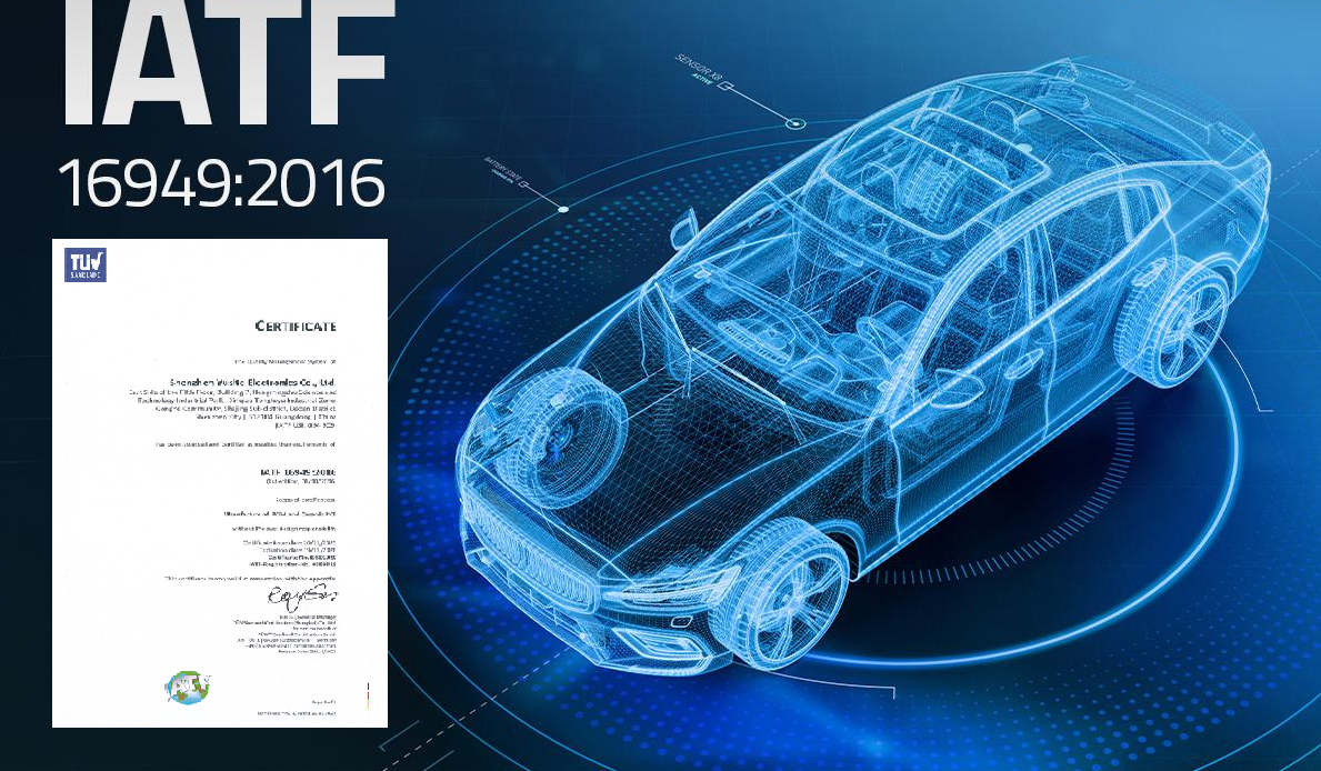
An IATF 16949 certified PCB is a printed circuit board manufactured under a quality management system that complies with IATF 16949, the global automotive industry standard that replaced ISO/TS 16949.
Unlike general ISO 9001 certification, IATF 16949 is automotive-specific and focuses on:
Defect prevention rather than detection
Risk-based process control
Continuous improvement throughout the supply chain
Traceability and accountability at every manufacturing stage
For PCB manufacturing, this means every processâfrom laminate sourcing and copper plating to imaging, drilling, surface finish, and final inspectionâis documented, controlled, audited, and continuously improved.
An IATF 16949 certified PCB supplier is qualified to support automotive OEMs, Tier 1 suppliers, and Tier 2 suppliers globally.
Typical Applications for IATF 16949 Certified PCBs
Automotive electronics operate in environments that are far more demanding than consumer or industrial electronics. As a result, IATF 16949 certified PCBs are widely used in systems where failure is unacceptable, like:
Electric vehicle (EV) systems â BMS, OBC, inverters, DC-DC converters
Body electronics â lighting control, window and seat modules
Chassis and safety systems â ABS, EPS, airbag controllers
These applications demand high reliability, thermal stability, and long service life, often exceeding 10â15 years.
Why IATF 16949 Certification Is Critical in Automotive Electronics?
Automotive PCBs must survive:
Temperature ranges from -40°C to +125°C or higher
Continuous vibration and mechanical shock
Long-term exposure to humidity, oils, and chemicals
10â20 years of operational life
IATF 16949 certification ensures that a PCB supplier has systems in place to manage these risks through:
APQP (Advanced Product Quality Planning) for new product introduction
FMEA (Failure Mode and Effects Analysis) to identify and mitigate risks
SPC (Statistical Process Control) to maintain consistency
Root cause analysis and corrective actions (8D, PDCA)
Supplier quality management for raw materials
Without IATF 16949, PCB quality may rely too heavily on final inspection rather than process stability, which is unacceptable for automotive use.
Does IATF 16949 Mean Zero Defects?
No quality standard can guarantee absolute zero defectsâbut IATF 16949 is designed to make defects rare, predictable, and preventable. Instead of reacting to failures, IATF 16949 requires:
Early risk identification
Process capability monitoring
Immediate corrective action when trends appear
Continuous reduction of variation
In practice, this leads to dramatically lower defect rates, improved field reliability, and reduced recall risk for automotive customers.
Does IATF Certification Automatically Mean Automotive Capability?
No, not always. IATF 16949 certifies the quality management system, not the technical capability alone.
A truly automotive-capable IATF 16949 certified PCB supplier must also demonstrate:
Experience with automotive-grade laminates (high Tg, low CTE, CAF-resistant)
Tight control of dielectric thickness and impedance
At EBest Circuit (Best Technology), our automotive PCBs are manufactured under a fully implemented IATF 16949 quality management system, ensuring process stability, traceability, and long-term reliability for safety-critical automotive electronics.
Automotive-grade epoxy, green / black / red (others on request)
Silkscreen
White, yellow (high contrast for traceability)
Panel Size
Up to 600 Ă 1200 mm
CAF Resistance
CAF-resistant material selection & process control
Thermal Reliability
Designed for â40°C to +125°C operating environments
Electrical Testing
Flying Probe Test, Fixture E-Test (100% testing)
Inspection
AOI, X-ray (for HDI & fine-pitch designs)
Reliability Testing
Thermal shock, thermal cycling (upon request)
Traceability
Full lot & material traceability per IATF 16949
Documentation Support
PPAP, Control Plan, PFMEA, SPC records
Our Services for IATF 16949 Certified PCB Projects
We provide comprehensive support throughout the product lifecycle:
Automotive PCB DFM and engineering review
Prototype, NPI, and mass production support
PPAP and quality documentation assistance
Long-term supply and lifecycle management
PCB & PCBA one-stop manufacturing solutions
Our goal is to help customers reduce risk, shorten development cycles, and scale confidently. If youâre searching for a dependable iatf 16949 certified pcb supplier, EBest Circuit (Best Technology) is ready to support your automotive electronics projects.
Frequently Asked Questions (FAQ)
1. Is IATF 16949 mandatory for automotive PCBs?
Most automotive OEMs and Tier 1 suppliers require IATF 16949 certification for PCB suppliers.
2. Can IATF 16949 certified suppliers support EV and ADAS projects?
Yes. IATF 16949 is widely adopted in EV, hybrid, and autonomous vehicle electronics.
3. Does IATF 16949 cover PCB assembly?
Only if PCBA is included in the certification scope. Always verify the certificate details.
4. How often is IATF 16949 audited?
Certified suppliers undergo annual surveillance audits and full recertification every three years.
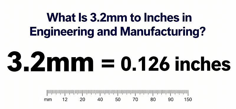
3.2mm to inches equals 0.12598 inches, commonly rounded to 0.126 inches.
lthough 3.2mm is often associated with 1/8 inch, it is slightly larger than 1/8″ (which equals 3.175mm). For general PCB fabrication, hardware selection, and sheet material, treating 3.2mm as â 1/8 inch is acceptable. For tight-tolerance or mating components, always use the exact value: 0.12598 inches.
This conversion is frequently referenced in PCB thickness control, mechanical part matching, and cross-standard manufacturing, especially when metric-designed components are produced or assembled in imperial-based environments.
Engineering Method for Converting 3.2mm to Inches
All engineering-grade conversions rely on a fixed constant.
1 inch = 25.4 millimeters (exact, not approximate)
To convert millimeters to inches:
3.2 Ă· 25.4 = 0.12598 inches
In CAD systems, CAM outputs, and inspection reports, engineers usually keep four to five decimal places to prevent cumulative dimensional deviation. Rounding is applied only at the documentation or purchasing stage.
Why 3.2mm Is Widely Used in PCB and Mechanical Manufacturing?
3.2mm is considered a hybrid-standard thickness. It bridges metric design logic with imperial production habits.
In PCB manufacturing, 3.2mm is commonly selected for:
Power distribution boards
Backplanes and structural PCBs
Boards used as mounting or support elements
Industrial controller PCBs requiring stiffness
In mechanical manufacturing, 3.2mm sheet thickness is frequently used for:
Aluminum and steel brackets
Equipment enclosures
Protective covers and panels
This thickness offers good rigidity while remaining compatible with standard drilling, routing, and bending processes.
3.2mm to Inches Chart ((Fractional & Decimal)
The table below shows 3.2mm to inches alongside nearby metric sizes, including fractional inch equivalents commonly used in hardware, PCB thickness, and metal stock selection.
Millimeters (mm)
Fractional Inches
Decimal Inches
2.0 mm
5/64″
0.0787″
2.4 mm
3/32″
0.0937″
3.2 mm
â 1/8″
0.12598″ (â 0.126″)
3.5 mm
9/64″
0.1378″
4.0 mm
5/32″
0.1575″
4.8 mm
3/16″
0.1890″
6.4 mm
1/4″
0.2520″
Engineering note:
1/8 inch equals 3.175mm, not 3.2mm. The 0.025mm difference may matter in precision machining, PCB slot sizing, or press-fit applications.
Why 3.2mm Is Commonly Treated as 1/8 Inch?
In practice, 3.2mm is widely treated as a nominal 1/8-inch equivalent because:
The dimensional difference is very small
Standard drill bits and tooling align closely
PCB thickness tolerances usually exceed ±0.025mm
Hardware and sheet stock are often sold by nominal size
This is why datasheets, BOMs, and supplier listings frequently group 3.2mm and 1/8 inch together.
3.2mm to cm in Technical Documentation
3.2mm equals 0.32 cm.
This conversion is exact and does not involve rounding. It is often used in:
Engineering specifications
International standards
Educational and training materials
Centimeter notation is common in documentation intended for non-manufacturing audiences.
3.2mm to Feet in Industrial Context
3.2mm equals 0.0105 feet.
While feet are rarely used for small dimensions, this conversion may appear in:
Mixed-unit architectural layouts
Legacy documentation
Facility-level mechanical references
For fabrication work, inches or millimeters remain preferred.
Is 3.2mm the Same as 1/8 Inch in PCB and Mechanical Design?
No. 1/8 inch equals 3.175mm, not 3.2mm.
The difference is 0.025mm, which may seem negligible but can impact:
PCB edge connector fit
Slot and cutout tolerances
Press-fit components
Stack-up alignment in assemblies
In high-reliability PCB designs, this difference must be evaluated rather than assumed acceptable.
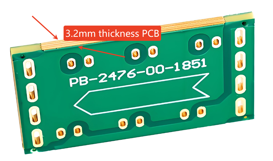
Practical PCB Applications of 3.2mm Thickness
In PCB fabrication, 3.2mm thickness is often chosen when mechanical strength is more important than weight reduction.
Typical PCB use cases include:
High-current power boards
Backplanes in industrial systems
PCBs acting as mechanical supports
Boards exposed to vibration or shock
Thicker boards reduce flexing, which helps protect solder joints and large components.
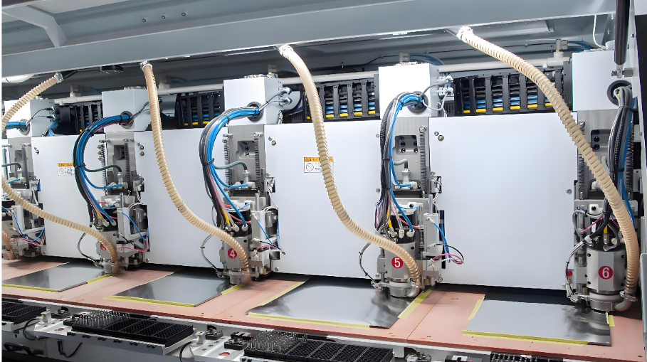
Manufacturing Implications of 3.2mm Thickness
From a production perspective, 3.2mm thickness affects multiple processes:
Drilling requires adjusted feed rates
Routing needs deeper cut passes
Plating thickness becomes more critical
Panel warpage control becomes more important
Manufacturers often adjust tooling and process parameters specifically for boards or parts at this thickness.
Metric vs Imperial Units in Global PCB Manufacturing
Most PCB designs originate in metric units. However, many:
Assembly fixtures
Test equipment
Mechanical interfaces
still follow imperial standards.
This creates frequent conversion scenarios where 3.2mm to inches must be clearly defined to avoid misinterpretation between design, fabrication, and assembly teams.
Common Engineering Errors When Converting 3.2mm to Inches
Errors often occur when:
Designers assume 3.2mm equals 1/8 inch
Finished thickness is confused with core thickness
Copper weight and surface finish are ignored
Units are converted without tolerance context
These mistakes can lead to fit issues, assembly delays, or rejected parts.
FAQs About 3.2mm to Inches
1. How many inches is 3.2mm?
3.2mm equals 0.12598 inches, which is commonly rounded to 0.126 inches for practical use. This value is widely accepted in engineering, PCB manufacturing, and hardware selection.
2. Is 3.2mm the same as 1/8 inch?
No. 3.2mm is slightly larger than 1/8 inch.
1/8 inch equals 3.175mm, while 3.2mm equals 0.12598 inches. The difference is small but can matter in precision applications.
3. Why is 3.2mm often called 1/8 inch?
3.2mm is often treated as 1/8 inch because the dimensional difference is minimal and usually falls within standard manufacturing tolerances. Many suppliers group these sizes together for convenience.
4. Is 3.2mm a standard PCB thickness?
Yes. 3.2mm is a common PCB thickness, especially for power boards, backplanes, and mechanically reinforced PCBs. It provides higher rigidity compared to thinner boards.
5. Can 3.2mm replace 1/8 inch material?
In most cases, yes.
For sheet metal, PCB panels, and brackets, 3.2mm can replace 1/8 inch. Always verify tolerance requirements for mating or press-fit parts.
6. What is the formula to convert 3.2mm to inches?
The formula is:
Inches = millimeters Ă· 25.4
3.2 Ă· 25.4 = 0.12598 inches
7. Does PCB copper thickness affect the final 3.2mm board thickness?
Yes. The finished PCB thickness includes laminate, copper layers, and surface finish. Copper weight and plating can slightly increase the final thickness beyond the nominal 3.2mm.
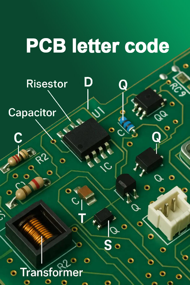
What Are PCB Letter Codes? â Definitions & Core Functions
PCB letter codes are essential identifiers used in printed circuit board (PCB) design and manufacturing, serving as a universal language to label components, layers, test points, and functional zones on a board. These PCB letter codes eliminate confusion during assembly, repair, and quality control, ensuring that engineers, technicians, and suppliers across the globe can quickly interpret a PCBâs layout and purpose. Whether youâre designing a new board, troubleshooting a faulty circuit, or sourcing replacement parts, understanding PCB letter codes is non-negotiable for streamlining processes and avoiding costly errors. Without clear, standardized letter codes, even simple tasks like identifying a resistor or navigating a multi-layer PCB would become time-consuming and error-prone.
International Standards & Design Specifications for PCB Letter Codes (IEEE/IPC Standards Explained)
When working with PCB letter codes, adherence to international standards is critical to ensure compatibility and clarity. The two most widely recognized standards are IEEE (Institute of Electrical and Electronics Engineers) and IPC (Association Connecting Electronics Industries), each outlining guidelines for consistent PCB letter codes usage. IEEE standards, such as IEEE 315, focus on component labeling conventions, while IPC standards like IPC-2221 detail general PCB design requirements, including letter code formatting for layers and test points. Following these standards ensures that your PCB letter codes are understandable to anyone working with the board, regardless of their location or industry. For example, IPC specifies that power-related components should use letter codes starting with âPâ (e.g., P1 for Power Connector), while IEEE mandates that resistors use âRâ (e.g., R12 for Resistor 12). Ignoring these standards can lead to miscommunication, delayed projects, and incompatible components.
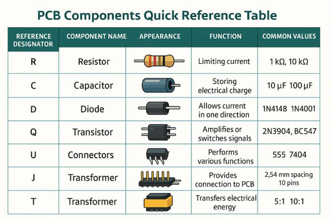
pcb code list (Comprehensive Common PCB Letter Codes Reference Table)
Having a reliable reference for common PCB letter codes saves time and reduces guesswork. Below is a complete, industry-aligned list of PCB letter codes (per IEEE 315 and IPC-2221 standards), covering passive components, active components, connectors, power elements, test points, and specialized parts:
This comprehensive PCB letter codes list covers 95% of components used in consumer electronics, industrial equipment, automotive PCBs, medical devices, and aerospace applications. For ultra-specialized use cases (e.g., military-grade PCBs), additional industry-specific codes may apply, but this table serves as the definitive reference for standard PCB design and manufacturing workflows.
pcb components identification (PCB Component Identification: Quick Mapping from Codes to Physical Parts)
Translating PCB letter codes to physical components requires a combination of visual inspection and basic knowledge of component types. Start by locating the printed letter code on the PCBâthis is typically printed near the component itself. Next, cross-reference the code with the list above to identify the component category (e.g., âCâ for capacitor). Then, use physical characteristics to confirm: resistors are often cylindrical or rectangular with color bands, capacitors are small and cylindrical or rectangular, and ICs are larger with multiple pins. For example, if you see âU06â on the board, youâll know to look for a multi-pin integrated circuit nearby. This PCB components identification process becomes faster with practice, but having a cheat sheet of PCB letter codes and component shapes will accelerate your workflow. For hard-to-identify components, use a digital multimeter to test functionality, which can confirm if a component matches its labeled code.
Numbering Rules for PCB Letter Codes (Sequential Numbering, Zonal Numbering, Multi-layer Board Numbering)
PCB letter codes arenât just random labelsâthey follow specific numbering rules to ensure organization and scalability. The three most common numbering systems are:
Sequential Numbering: This is the simplest method, where components are numbered in the order theyâre placed on the PCB (e.g., R01, R02, R03âŠ). Itâs ideal for small, simple PCBs with few components.
Zonal Numbering: For larger PCBs, components are grouped by zone (e.g., top-left, power section) and numbered within each zone (e.g., R101 for Resistor in Zone 1, Position 1; R205 for Resistor in Zone 2, Position 5). This makes it easier to locate components in complex layouts.
Multi-layer Board Numbering: Multi-layer PCBs add a layer identifier to the code (e.g., R3-09 for Resistor on Layer 3, Position 9). This is critical for distinguishing components on different layers, which is essential during assembly and repair.
Understanding these PCB letter codes numbering rules helps you navigate any PCB design, whether itâs a small hobby board or a large industrial PCB. Consistency in numbering also ensures that your PCB letter codes are compatible with CAD software and manufacturing processes.
Detailed Explanation of Special-Function PCB Letter Codes (Power Supply, Test Points, Interface Codes)
Beyond standard component labels, PCB letter codes include special-function codes for critical board features. These codes are designed to highlight important areas and simplify maintenance:
Power Supply Codes: These start with âPâ (e.g., P3V3 for 3.3V Power Rail, P5V for 5V Power Rail) and indicate voltage levels or power distribution points. Theyâre vital for avoiding short circuits and ensuring proper power delivery.
Test Point Codes: Labeled with âTPâ (e.g., TP_VIN for Input Voltage Test Point, TP_GND for Ground Test Point), these codes mark points where technicians can measure signals or voltages during testing. They eliminate the need to probe sensitive components directly.
Interface Codes: These identify external connections, such as âUSB1â for USB Port 1, âETH0â for Ethernet Port 0, or âHDMI2â for HDMI Port 2. They make it easy to map external devices to the PCBâs internal circuitry.
Mastering these special-function PCB letter codes is key for anyone involved in PCB testing, repair, or system integration. They reduce the risk of mistakes and make complex boards more manageable.
Recommended Practical Tools & Resources for Decoding PCB Letter Codes
Decoding PCB letter codes becomes even easier with the right tools and resources. Here are our top recommendations for both beginners and professionals:
Digital Multimeters: A basic multimeter can test components (e.g., resistors, capacitors) to confirm their identity, complementing the letter code label.
PCB CAD Software: Tools like Altium Designer, KiCad, or Eagle include built-in PCB letter codes libraries and validation features to ensure compliance with standards.
Online Databases: Websites like IPCâs standards library or IEEE Xplore provide access to official PCB letter codes specifications for advanced users.
Mobile Apps: Apps like âPCB Component Identifierâ or âElectronics Referenceâ offer on-the-go access to PCB letter codes lists and component identification guides.
These tools streamline the process of working with PCB letter codes, whether youâre in the office, workshop, or field. Investing in reliable resources will save you time and improve the accuracy of your work.
3 Core Tips for Beginners to Master PCB Letter Codes Quickly
If youâre new to PCB letter codes, these three tips will help you master them in no time:
Memorize High-Frequency Codes: Start by learning the most common codes (R, C, D, U, J) since they appear on nearly every PCB. Write them down or use flashcards for quick recall.
Practice with Real PCBs: Grab old electronics (e.g., smartphones, routers) and identify components using their PCB letter codes. This hands-on practice is far more effective than just reading lists.
Stick to Standards: Always reference IEEE or IPC standards when working with PCB letter codes. Avoid creating custom codes unless absolutely necessary, as this can cause confusion for others.
By focusing on these fundamentals, youâll build confidence and proficiency with PCB letter codes in weeks, not months.
Application Cases of PCB Letter Codes in Different Scenarios (Repair, Design, Procurement)
PCB letter codes are versatile and used across multiple stages of the PCB lifecycle. Here are real-world examples of how theyâre applied:
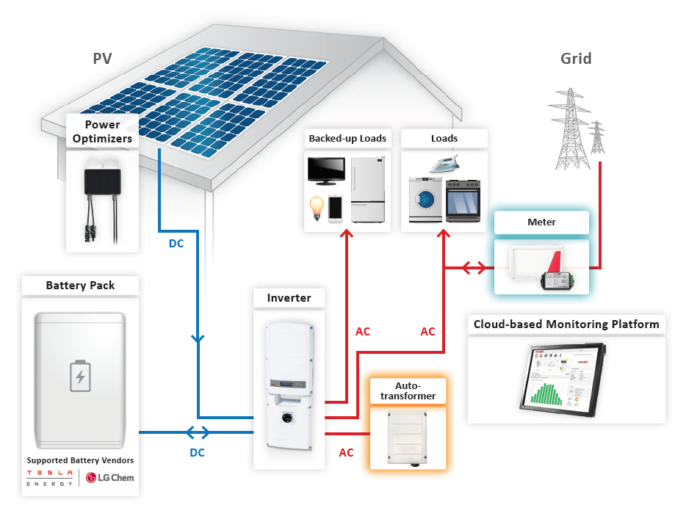
Repair: A technician troubleshooting a faulty TV PCB sees the code âQ04â near a burnt component. Using the PCB letter codes list, they identify it as a transistor, source a replacement, and fix the issue in minutes.
Design: An engineer designing a medical device PCB uses zonal numbering for PCB letter codes (e.g., R302 for Resistor in the Sensor Zone). This helps the assembly team quickly locate components and ensures compliance with regulatory standards.
Procurement: A buyer sourcing components for a production run references the PCB letter codes on the bill of materials (BOM) to order the correct resistors (R01-R50) and capacitors (C01-C35). This eliminates ordering errors and delays.
In each scenario, PCB letter codes improve efficiency, reduce mistakes, and ensure clear communication between teams.
Common Misunderstandings & Pitfalls of PCB Letter Codes
Even experienced professionals can fall prey to misunderstandings when working with PCB letter codes. Here are the most common pitfalls to avoid:
Ignoring Standard Differences: Assuming IEEE and IPC PCB letter codes are identical is a mistake. For example, some IPC codes for test points differ from IEEE, so always confirm which standard the PCB uses.
Custom Code Overload: Creating too many custom PCB letter codes for specialized components can make the board unreadable to others. Use custom codes sparingly and document them clearly.
Poor Placement: Printing PCB letter codes too close to components or in hard-to-see areas (e.g., under large ICs) makes them useless. Ensure codes are visible and easily accessible.

Inconsistent Numbering: Mixing sequential and zonal numbering on the same PCB causes confusion. Stick to one system throughout the design.
By avoiding these pitfalls, youâll ensure that your PCB letter codes are effective and user-friendly.
FAQ: Frequently Asked Questions About PCB Letter Codes
Q1: Do different manufacturers use different PCB letter codes?
A1: While most manufacturers follow IEEE or IPC standards for PCB letter codes, some may use custom variations for specialized products. Always check the PCBâs datasheet or consult the manufacturer if you encounter unfamiliar codes.
Q2: Whatâs the difference between PCB letter codes for single-layer and multi-layer boards?
A2: Multi-layer boards add a layer identifier to PCB letter codes (e.g., R2-07 for Layer 2, Resistor 7), while single-layer boards use simple sequential or zonal numbering. This layer distinction is critical for assembly and repair.
Q3: I canât find a matching component for a PCB letter codeâwhat should I do?
A3: First, confirm the standard (IEEE/IPC) used for the PCB letter codes. If the code is still unrecognizable, check the PCBâs BOM or contact the original equipment manufacturer (OEM) for clarification. You can also use a component tester to identify the partâs function.
Q4: Can I create my own PCB letter codes for a custom project?
A4: You can, but itâs not recommended unless the project is for personal use. Custom PCB letter codes can cause confusion for anyone else working on the board. If you must use custom codes, document them clearly and share the reference with your team.


Q5: Are PCB letter codes required for small hobby PCBs?
A5: Theyâre not mandatory, but using PCB letter codes on hobby PCBs is a good practice. It makes assembly easier, helps with troubleshooting, and prepares you for professional projects where codes are standard.
Q6: How do I handle conflicting PCB letter codes on a board?
A6: Conflicting codes (e.g., two components labeled âR05â) usually indicate a design error. Cross-reference the PCB with the BOM to confirm the correct labels, and contact the designer or manufacturer to resolve the issue before proceeding with assembly or repair.
Conclusion: Efficient Application Methodology for PCB Letter Codes
PCB letter codes are the backbone of clear communication in PCB design, manufacturing, and maintenance. By understanding their definitions, following international standards, using practical tools, and learning from real-world applications, you can leverage PCB letter codes to streamline your workflow, reduce errors, and improve collaboration. Whether youâre a beginner or a seasoned professional, mastering these codes is essential for success in the electronics industry.
If youâre in need of high-quality PCBs with accurate, standardized PCB letter codes that meet IEEE and IPC standards, look no further. We specialize in manufacturing custom PCBs tailored to your specific needs, with clear PCB letter codes that simplify assembly, repair, and compliance. Donât let confusing or inconsistent codes slow down your projectâplace your order today by emailing us at sales@bestpcbs.com. Our team is ready to deliver reliable, industry-compliant PCBs that meet your deadlines and exceed your expectations.
How Can Some Inductors be Active and Others Passive? An inductor is traditionally viewed as a passive part that stores energy in a magnetic field. Yet engineers often encounter the term âactive inductorâ in RF design, analog circuits, and integrated systems. This raises a natural question: how can an inductor be both passive and active?
The answer lies in understanding the physical nature of real inductors and how active circuits replicate inductive behavior using transistors. Both serve important roles, but for very different reasons.
What Defines a Passive vs Active Component?
A passive componentdoes not generate or amplify energy. It reacts directly to the applied electrical stimulus and cannot increase a signalâs power. Examples include resistors, capacitors, and classical inductors. They contribute predictable impedance but do not require an external power rail.
Active components, such as transistors, op-amps, and ICs, control current flow and may provide amplification or buffering. They need supply voltage and can introduce gain, shaping the signal beyond what passive parts can offer.
Understanding this boundary clarifies the discussion: a real inductor made from a coil is always passive. A circuit that imitates an inductor using active devices can appear inductive, but it is not passive. If you want to know more about active vs passive components, you can read our another post: Key differences between active and passive components
Are Inductors Active or Passive?
Inductors are passive components. A real inductor does not need an external power supply and cannot amplify signalsâit simply stores energy in a magnetic field when current passes through it. Because it neither generates nor controls power using another energy source, it is classified as a passive device in electronics.
However, in modern RF and integrated circuit design, you may encounter the term active inductor, which can cause confusion. These are not physical coils but transistor-based circuits that imitate the behavior of an inductor. Since they require external power and use active devices like MOSFETs or BJTs to create inductive reactance, they are considered âactive.â So while true inductors are always passive, engineers sometimes build circuits that behave like inductors using active components.
Why Inductors Are Classified as Passive Components?
The behavior of a physical inductor is rooted in fundamental electromagnetic principles. When current flows through a coil, a magnetic field forms. As the current changes, the magnetic field changes, resisting that shift. This energy exchange happens without any external power source.
A real inductor is therefore passive because:
It can store energy but does not create energy.
It influences current change without external power.
It cannot add gain to any signal path.
It operates based solely on electromagnetic induction.
Even in complex designs such as buck converters or class-D amplifiers, the inductor simply reacts to switch transitions and waveform shapes created by active devices. All âdynamicâ behavior is still passive in nature.
How Does an Inductor Act at T 0+ and T â?
At T = 0âș, an inductor behaves like a short-term open circuit because it resists any sudden change in current. The moment a voltage is applied, the current through the inductor starts at zero and increases gradually, so the inductor initially blocks current flow as if it were an open switch.
At T = â, an inductor behaves like a short circuit because once the current reaches a steady state, the inductor no longer opposes it. The stored magnetic field becomes constant, the inductorâs voltage drops to zero, and it effectively acts as a piece of wire with minimal resistance.
Why Some Inductors Appear âActiveâ in Switching Power Circuits?
In switching circuits, an inductor often behaves in a way that looks purposeful and controlledâalmost like an active element. For example:
In a buck converter, the inductor ramps current up and down in sync with the MOSFET switching.
In a boost converter, the inductor releases stored energy to lift the voltage.
In a flyback design, the inductor (transformer primary) delivers energy during off-time.
This controlled energy delivery can seem active. But the inductor remains passive because:
It performs no amplification.
It has no supply pins.
All action results from controlled switching around it.
The inductor is only following physics. Its âactive-lookingâ behavior is driven by the switching controller, not the inductor itself.
How Active Inductors Work?
Active inductors exist because integrated circuits cannot easily include large, high-quality coils. Instead, designers use transistors and feedback networks to replicate inductive reactance.
Common active inductor approaches:
Gyrator circuits: Create an inductive response using a capacitor and an active device.
MOSFET-based inductors: Leverage transconductance to shape current like a coil would.
Gm-C active filters: Combine tunable transconductance with capacitors for high-frequency inductive behavior.
Active inductors rely on:
Bias current
Voltage gain
Feedback loops
These elements allow the circuit to emulate inductance over a chosen frequency range. They do not store energy magnetically; instead, they reproduce the impedance profile of an inductor electrically.
How to Tell Whether an Inductor Is Passive or âActive-Likeâ?
The simplest way is to examine its structure or schematic.
A passive inductor:
Contains a coil of copper wire.
May use ferrite, iron, or air as the core.
Has no power supply pins.
Always presents inductive reactance at AC.
Stores energy in a real magnetic field.
An active inductor:
Includes MOSFETs, BJTs, resistors, and capacitors.
Requires biasing from VCC or VDD.
Does not behave like an inductor at DC.
Mimics inductance only across a designed range.
Does not produce a true magnetic field.
If it physically coils wire, it is passive. If it needs biasing, it is active.
Why Use Active Inductors Instead of Passive Ones?
Engineers select active inductors for reasons tied to integration, size, and flexibility. A real inductor may be too large, too costly, or incompatible with an integrated CMOS flow. Active versions offer:
Very small footprint for RF ICs and SoCs.
Electronically adjustable inductance for tunable filters.
Higher effective inductance than what is possible in a small coil.
Better integration on silicon with no magnetics required.
Lower parasitics compared with some wound inductors.
This makes active inductors popular in:
RF front-ends
On-chip matching networks
Integrated oscillators
Bluetooth, Wi-Fi, and mmWave circuits
Adaptive analog systems
Why Passive Inductors Are Still Needed?
Although active inductors are flexible, they cannot replace wound inductors when real magnetic energy storage or high linearity is required. Passive inductors excel in:
Energy transfer systems
Power converters
High-current paths
EMI suppression
Resonant circuits with high Q
Audio crossover networks
RF circuits where low noise is important
Passive inductors also work over a broad frequency range and do not rely on bias currents. They withstand much higher power levels than active circuits.
When Should You Use a Passive Inductor?
A passive inductor is the correct choice when the application needs real, physical energy handling. Use one when the design involves:
Power conversion
DC-DC regulation
Motor control circuits
High-current feeding
RF filters needing high Q
Low-noise front-end requirements
When reliability, linearity, and energy efficiency matter, a real inductor is essential.
When Should You Use an Active Inductor?
Active inductors become practical when design priorities shift:
The circuit must be fully integrated on a chip.
Board space is extremely limited.
Tunability is required through voltage or current adjustments.
Only small-signal behavior matters, not high power.
The circuitâs operating band is narrow, such as RF.
If the goal is impedance shaping, not energy transport, an active inductor offers a compact and configurable solution.
Conclusion
A traditional inductor with a wire coil is always passive. It stores energy in a magnetic field and cannot amplify signals. Active inductors, on the other hand, are transistor-based circuits that imitate inductive behavior using gain and feedback. They are âactiveâ because they need power and introduce controlled impedance rather than storing energy.
Both types play important roles in electronics. Understanding their differences helps engineers select the right component for RF filters, switching regulators, mixed-signal ICs, and miniaturized platforms where performance, size, and frequency all shape design strategy.
This website uses cookies to enhance your experience, remember your preferences, and help us understand how visitors use our site. You can accept all cookies, reject non-essential cookies, or manage your settings.
This website uses cookies to improve your experience while you navigate through the website. Out of these cookies, the cookies that are categorized as necessary are stored on your browser as they are essential for the working of basic functionalities of the website. We also use third-party cookies that help us analyze and understand how you use this website. These cookies will be stored in your browser only with your consent. You also have the option to opt-out of these cookies. But opting out of some of these cookies may have an effect on your browsing experience.
Necessary cookies are absolutely essential for the website to function properly. These cookies ensure basic functionalities and security features of the website, anonymously.
Cookie
Duration
Description
cookielawinfo-checkbox-analytics
11 months
This cookie is set by GDPR Cookie Consent plugin. The cookie is used to store the user consent for the cookies in the category "Analytics".
cookielawinfo-checkbox-functional
11 months
The cookie is set by GDPR cookie consent to record the user consent for the cookies in the category "Functional".
cookielawinfo-checkbox-necessary
11 months
This cookie is set by GDPR Cookie Consent plugin. The cookies is used to store the user consent for the cookies in the category "Necessary".
cookielawinfo-checkbox-others
11 months
This cookie is set by GDPR Cookie Consent plugin. The cookie is used to store the user consent for the cookies in the category "Other.
cookielawinfo-checkbox-performance
11 months
This cookie is set by GDPR Cookie Consent plugin. The cookie is used to store the user consent for the cookies in the category "Performance".
viewed_cookie_policy
11 months
The cookie is set by the GDPR Cookie Consent plugin and is used to store whether or not user has consented to the use of cookies. It does not store any personal data.
Functional cookies help to perform certain functionalities like sharing the content of the website on social media platforms, collect feedbacks, and other third-party features.
Performance cookies are used to understand and analyze the key performance indexes of the website which helps in delivering a better user experience for the visitors.
Analytical cookies are used to understand how visitors interact with the website. These cookies help provide information on metrics the number of visitors, bounce rate, traffic source, etc.
Advertisement cookies are used to provide visitors with relevant ads and marketing campaigns. These cookies track visitors across websites and collect information to provide customized ads.