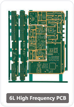
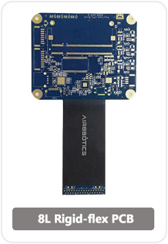
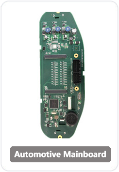
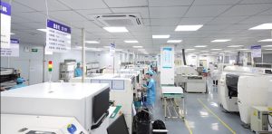
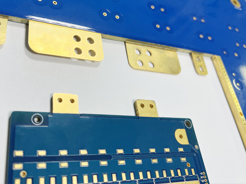
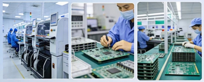
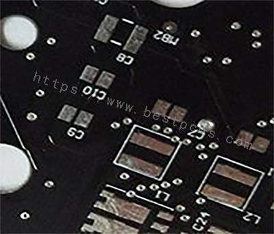
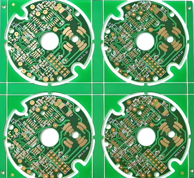
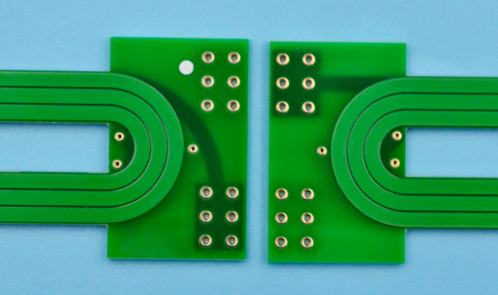
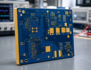
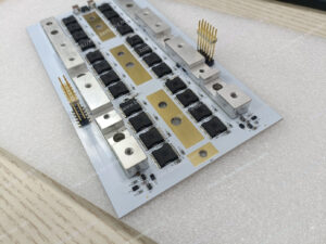
This certification confirms that PCB processes are controlled, repeatable, and audited for defect prevention rather than post-inspection.
For automotive buyers, choosing an IATF 16949 certified PCB supplier directly reduces recall risk, audit pressure, and long-term field failures.
What Is an IATF 16949 Certified PCB Supplier?
AnIATF 16949 certified PCB supplier is a PCB manufacturer that complies with the global automotive quality management standard issued by the International Automotive Task Force.
This standard requires:
Full process traceability
Preventive quality planning (APQP, FMEA)
Continuous improvement and corrective action systems
Controlled production from prototype to mass volume
Unlike general certifications, IATF 16949 applies only to automotive supply chains.
What Is an IATF 16949 Certified PCB Supplier?
Why Do Automotive OEMs Require IATF 16949 PCB Suppliers?
Automotive OEMs require IATF 16949 because PCB failures can trigger recalls, safety risks, and regulatory penalties.
This certification ensures:
Stable PCB manufacturing processes
Early risk identification
Consistent quality across production lots
Audit-ready documentation for OEM and Tier-1 reviews
For safety-critical electronics, uncertified suppliers introduce unacceptable risk.
Which Automotive PCBs Must Come from an IATF 16949 Certified Factory?
Automotive PCBs that typically require IATF 16949 certification include:
Engine control units (ECU)
ADAS and camera modules
Radar and RF automotive PCBs
Battery management systems (BMS)
Power inverter and motor control boards
Safety and braking control electronics
If a PCB affects vehicle safety, emissions, or power control, certification is expected.
IATF 16949 vs ISO 9001 for PCB Manufacturing
ISO 9001 focuses on general quality procedures across industries. IATF 16949 focuses on automotive risk prevention and process stability.
Key differences for PCB buyers:
IATF 16949 requires FMEA and PPAP
ISO 9001 allows broader process variation
IATF 16949 enforces corrective action with data
ISO 9001 emphasizes documentation, not automotive reliability
ISO 9001 alone is not sufficient for automotive PCBs.
Core Capabilities Required from an IATF 16949 PCB Supplier
An automotive-qualified PCB supplier must demonstrate both engineering and process discipline.
This includes impedance-controlled stackups, material consistency, SPC monitoring, and documented change control.
Below is a technical capability table automotive buyers often request.
Capability Category
Automotive PCB Requirement
Typical Specification Range
PCB Layer Count
Multilayer & HDI
2â20 layers
Controlled Impedance
Mandatory for high-speed / RF
±5% to ±10%
Copper Thickness
Power and signal balance
0.5â6 oz
Minimum Trace / Space
Dense automotive layouts
3/3 mil
Via Technology
Reliability under vibration
Through, blind, buried, microvia
Laminate Materials
Thermal and electrical stability
High-Tg FR-4, Rogers, hybrid stackups
Surface Finish
Automotive solderability
ENIG, ENEPIG, OSP
Operating Temperature
Harsh environment tolerance
â40°C to +125°C
Traceability System
Mandatory under IATF 16949
Lot-level MES tracking
Quality Documentation
OEM audit compliance
PPAP, FMEA, Control Plan, SPC
Production Volume
Prototype to mass production
NPI â high volume
Reliability Testing
Automotive qualification
Thermal cycling, cross-section
How Traceability Works in IATF 16949 PCB Manufacturing?
In IATF 16949 certified PCB manufacturing, traceability links each PCB lot to materials, processes, inspections, and operators.
Traceability systems typically record:
Laminate batch numbers
Inner layer imaging data
Lamination cycles
Plating and surface finish parameters
Final inspection results
This allows fast containment if field issues occur.
What Quality Risks Exist Without an IATF 16949 PCB Supplier?
Choosing a non-certified PCB supplier increases:
Process variation
Incomplete documentation
Poor root-cause analysis
Audit failures during OEM reviews
These risks often surface only after volume production begins.
What Documents Should an IATF 16949 PCB Supplier Provide?
Automotive buyers should expect:
PPAP documentation
PFMEA and Control Plans
Material certifications
SPC and inspection reports
Change management records
Missing documents usually indicate limited automotive readiness.
Prototype vs Mass Production: What Buyers Often Overlook
IATF 16949 applies from the prototype stage, not only mass production.
Controlled materials, documented changes, and engineering approvals must begin early. Skipping these steps creates instability during ramp-up.
Automotive-ready PCB suppliers treat prototypes as production-intent builds.
Why Automotive Buyers Choose EBest Circuit (Best Technology) as Their IATF 16949 Certified PCB Supplier?
EBest Circuit (Best Technology) supports automotive PCB projects under IATF 16949, ISO 9001, and ISO 13485, AS9100D systems.
Our company delivers:
Automotive-grade multilayer and HDI PCBs
Controlled impedance and high-frequency designs
MES-based traceability
Structured documentation for OEM audits
Smooth transition from prototype to mass production
This combination reduces buyer risk and accelerates project approval.
FAQs
1. Is IATF 16949 mandatory for automotive PCBs?
Yes, for OEM and safety-critical automotive electronics.
2. Does IATF 16949 cover PCB prototypes?
Yes. Process control applies from early builds.
3. Can ISO 9001 replace IATF 16949?
No. ISO 9001 alone does not meet automotive standards.
4. How can buyers verify IATF 16949 certification?
Check the certificate scope, issuing body, and audit validity.
5. Why is traceability critical in automotive PCBs?
It enables fast containment and root-cause analysis during failures.
Selecting an IATF 16949 certified PCB supplier is not just a purchasing decisionâit is a risk management strategy for automotive electronics. With vehicles increasingly dependent on electronics for safety, performance, and connectivity, PCB quality directly impacts system reliability and brand reputation.
This in-depth guide explains what IATF 16949 certification means for PCB manufacturing, how it affects automotive applications, how to evaluate certified suppliers, and why EBest Circuit (Best Technology) is a trusted partner for automotive PCB projects.
What Is an IATF 16949 Certified PCB?
An IATF 16949 certified PCB is a printed circuit board manufactured under a quality management system that complies with IATF 16949, the global automotive industry standard that replaced ISO/TS 16949.
Unlike general ISO 9001 certification, IATF 16949 is automotive-specific and focuses on:
Defect prevention rather than detection
Risk-based process control
Continuous improvement throughout the supply chain
Traceability and accountability at every manufacturing stage
For PCB manufacturing, this means every processâfrom laminate sourcing and copper plating to imaging, drilling, surface finish, and final inspectionâis documented, controlled, audited, and continuously improved.
An IATF 16949 certified PCB supplier is qualified to support automotive OEMs, Tier 1 suppliers, and Tier 2 suppliers globally.
Typical Applications for IATF 16949 Certified PCBs
Automotive electronics operate in environments that are far more demanding than consumer or industrial electronics. As a result, IATF 16949 certified PCBs are widely used in systems where failure is unacceptable, like:
Electric vehicle (EV) systems â BMS, OBC, inverters, DC-DC converters
Body electronics â lighting control, window and seat modules
Chassis and safety systems â ABS, EPS, airbag controllers
These applications demand high reliability, thermal stability, and long service life, often exceeding 10â15 years.
Why IATF 16949 Certification Is Critical in Automotive Electronics?
Automotive PCBs must survive:
Temperature ranges from -40°C to +125°C or higher
Continuous vibration and mechanical shock
Long-term exposure to humidity, oils, and chemicals
10â20 years of operational life
IATF 16949 certification ensures that a PCB supplier has systems in place to manage these risks through:
APQP (Advanced Product Quality Planning) for new product introduction
FMEA (Failure Mode and Effects Analysis) to identify and mitigate risks
SPC (Statistical Process Control) to maintain consistency
Root cause analysis and corrective actions (8D, PDCA)
Supplier quality management for raw materials
Without IATF 16949, PCB quality may rely too heavily on final inspection rather than process stability, which is unacceptable for automotive use.
Does IATF 16949 Mean Zero Defects?
No quality standard can guarantee absolute zero defectsâbut IATF 16949 is designed to make defects rare, predictable, and preventable. Instead of reacting to failures, IATF 16949 requires:
Early risk identification
Process capability monitoring
Immediate corrective action when trends appear
Continuous reduction of variation
In practice, this leads to dramatically lower defect rates, improved field reliability, and reduced recall risk for automotive customers.
Does IATF Certification Automatically Mean Automotive Capability?
No, not always. IATF 16949 certifies the quality management system, not the technical capability alone.
A truly automotive-capable IATF 16949 certified PCB supplier must also demonstrate:
Experience with automotive-grade laminates (high Tg, low CTE, CAF-resistant)
Tight control of dielectric thickness and impedance
At EBest Circuit (Best Technology), our automotive PCBs are manufactured under a fully implemented IATF 16949 quality management system, ensuring process stability, traceability, and long-term reliability for safety-critical automotive electronics.
Automotive-grade epoxy, green / black / red (others on request)
Silkscreen
White, yellow (high contrast for traceability)
Panel Size
Up to 600 Ă 1200 mm
CAF Resistance
CAF-resistant material selection & process control
Thermal Reliability
Designed for â40°C to +125°C operating environments
Electrical Testing
Flying Probe Test, Fixture E-Test (100% testing)
Inspection
AOI, X-ray (for HDI & fine-pitch designs)
Reliability Testing
Thermal shock, thermal cycling (upon request)
Traceability
Full lot & material traceability per IATF 16949
Documentation Support
PPAP, Control Plan, PFMEA, SPC records
Our Services for IATF 16949 Certified PCB Projects
We provide comprehensive support throughout the product lifecycle:
Automotive PCB DFM and engineering review
Prototype, NPI, and mass production support
PPAP and quality documentation assistance
Long-term supply and lifecycle management
PCB & PCBA one-stop manufacturing solutions
Our goal is to help customers reduce risk, shorten development cycles, and scale confidently. If youâre searching for a dependable iatf 16949 certified pcb supplier, EBest Circuit (Best Technology) is ready to support your automotive electronics projects.
Frequently Asked Questions (FAQ)
1. Is IATF 16949 mandatory for automotive PCBs?
Most automotive OEMs and Tier 1 suppliers require IATF 16949 certification for PCB suppliers.
2. Can IATF 16949 certified suppliers support EV and ADAS projects?
Yes. IATF 16949 is widely adopted in EV, hybrid, and autonomous vehicle electronics.
3. Does IATF 16949 cover PCB assembly?
Only if PCBA is included in the certification scope. Always verify the certificate details.
4. How often is IATF 16949 audited?
Certified suppliers undergo annual surveillance audits and full recertification every three years.
3.2mm to inches equals 0.12598 inches, commonly rounded to 0.126 inches.
lthough 3.2mm is often associated with 1/8 inch, it is slightly larger than 1/8″ (which equals 3.175mm). For general PCB fabrication, hardware selection, and sheet material, treating 3.2mm as â 1/8 inch is acceptable. For tight-tolerance or mating components, always use the exact value: 0.12598 inches.
This conversion is frequently referenced in PCB thickness control, mechanical part matching, and cross-standard manufacturing, especially when metric-designed components are produced or assembled in imperial-based environments.
Engineering Method for Converting 3.2mm to Inches
All engineering-grade conversions rely on a fixed constant.
1 inch = 25.4 millimeters (exact, not approximate)
To convert millimeters to inches:
3.2 Ă· 25.4 = 0.12598 inches
In CAD systems, CAM outputs, and inspection reports, engineers usually keep four to five decimal places to prevent cumulative dimensional deviation. Rounding is applied only at the documentation or purchasing stage.
Why 3.2mm Is Widely Used in PCB and Mechanical Manufacturing?
3.2mm is considered a hybrid-standard thickness. It bridges metric design logic with imperial production habits.
In PCB manufacturing, 3.2mm is commonly selected for:
Power distribution boards
Backplanes and structural PCBs
Boards used as mounting or support elements
Industrial controller PCBs requiring stiffness
In mechanical manufacturing, 3.2mm sheet thickness is frequently used for:
Aluminum and steel brackets
Equipment enclosures
Protective covers and panels
This thickness offers good rigidity while remaining compatible with standard drilling, routing, and bending processes.
3.2mm to Inches Chart ((Fractional & Decimal)
The table below shows 3.2mm to inches alongside nearby metric sizes, including fractional inch equivalents commonly used in hardware, PCB thickness, and metal stock selection.
Millimeters (mm)
Fractional Inches
Decimal Inches
2.0 mm
5/64″
0.0787″
2.4 mm
3/32″
0.0937″
3.2 mm
â 1/8″
0.12598″ (â 0.126″)
3.5 mm
9/64″
0.1378″
4.0 mm
5/32″
0.1575″
4.8 mm
3/16″
0.1890″
6.4 mm
1/4″
0.2520″
Engineering note:
1/8 inch equals 3.175mm, not 3.2mm. The 0.025mm difference may matter in precision machining, PCB slot sizing, or press-fit applications.
Why 3.2mm Is Commonly Treated as 1/8 Inch?
In practice, 3.2mm is widely treated as a nominal 1/8-inch equivalent because:
The dimensional difference is very small
Standard drill bits and tooling align closely
PCB thickness tolerances usually exceed ±0.025mm
Hardware and sheet stock are often sold by nominal size
This is why datasheets, BOMs, and supplier listings frequently group 3.2mm and 1/8 inch together.
3.2mm to cm in Technical Documentation
3.2mm equals 0.32 cm.
This conversion is exact and does not involve rounding. It is often used in:
Engineering specifications
International standards
Educational and training materials
Centimeter notation is common in documentation intended for non-manufacturing audiences.
3.2mm to Feet in Industrial Context
3.2mm equals 0.0105 feet.
While feet are rarely used for small dimensions, this conversion may appear in:
Mixed-unit architectural layouts
Legacy documentation
Facility-level mechanical references
For fabrication work, inches or millimeters remain preferred.
Is 3.2mm the Same as 1/8 Inch in PCB and Mechanical Design?
No. 1/8 inch equals 3.175mm, not 3.2mm.
The difference is 0.025mm, which may seem negligible but can impact:
PCB edge connector fit
Slot and cutout tolerances
Press-fit components
Stack-up alignment in assemblies
In high-reliability PCB designs, this difference must be evaluated rather than assumed acceptable.
Practical PCB Applications of 3.2mm Thickness
In PCB fabrication, 3.2mm thickness is often chosen when mechanical strength is more important than weight reduction.
Typical PCB use cases include:
High-current power boards
Backplanes in industrial systems
PCBs acting as mechanical supports
Boards exposed to vibration or shock
Thicker boards reduce flexing, which helps protect solder joints and large components.
Manufacturing Implications of 3.2mm Thickness
From a production perspective, 3.2mm thickness affects multiple processes:
Drilling requires adjusted feed rates
Routing needs deeper cut passes
Plating thickness becomes more critical
Panel warpage control becomes more important
Manufacturers often adjust tooling and process parameters specifically for boards or parts at this thickness.
Metric vs Imperial Units in Global PCB Manufacturing
Most PCB designs originate in metric units. However, many:
Assembly fixtures
Test equipment
Mechanical interfaces
still follow imperial standards.
This creates frequent conversion scenarios where 3.2mm to inches must be clearly defined to avoid misinterpretation between design, fabrication, and assembly teams.
Common Engineering Errors When Converting 3.2mm to Inches
Errors often occur when:
Designers assume 3.2mm equals 1/8 inch
Finished thickness is confused with core thickness
Copper weight and surface finish are ignored
Units are converted without tolerance context
These mistakes can lead to fit issues, assembly delays, or rejected parts.
FAQs About 3.2mm to Inches
1. How many inches is 3.2mm?
3.2mm equals 0.12598 inches, which is commonly rounded to 0.126 inches for practical use. This value is widely accepted in engineering, PCB manufacturing, and hardware selection.
2. Is 3.2mm the same as 1/8 inch?
No. 3.2mm is slightly larger than 1/8 inch.
1/8 inch equals 3.175mm, while 3.2mm equals 0.12598 inches. The difference is small but can matter in precision applications.
3. Why is 3.2mm often called 1/8 inch?
3.2mm is often treated as 1/8 inch because the dimensional difference is minimal and usually falls within standard manufacturing tolerances. Many suppliers group these sizes together for convenience.
4. Is 3.2mm a standard PCB thickness?
Yes. 3.2mm is a common PCB thickness, especially for power boards, backplanes, and mechanically reinforced PCBs. It provides higher rigidity compared to thinner boards.
5. Can 3.2mm replace 1/8 inch material?
In most cases, yes.
For sheet metal, PCB panels, and brackets, 3.2mm can replace 1/8 inch. Always verify tolerance requirements for mating or press-fit parts.
6. What is the formula to convert 3.2mm to inches?
The formula is:
Inches = millimeters Ă· 25.4
3.2 Ă· 25.4 = 0.12598 inches
7. Does PCB copper thickness affect the final 3.2mm board thickness?
Yes. The finished PCB thickness includes laminate, copper layers, and surface finish. Copper weight and plating can slightly increase the final thickness beyond the nominal 3.2mm.
What Are PCB Letter Codes? â Definitions & Core Functions
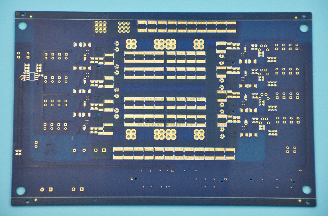
PCB letter codes are essential identifiers used in printed circuit board (PCB) design and manufacturing, serving as a universal language to label components, layers, test points, and functional zones on a board. These PCB letter codes eliminate confusion during assembly, repair, and quality control, ensuring that engineers, technicians, and suppliers across the globe can quickly interpret a PCBâs layout and purpose. Whether youâre designing a new board, troubleshooting a faulty circuit, or sourcing replacement parts, understanding PCB letter codes is non-negotiable for streamlining processes and avoiding costly errors. Without clear, standardized letter codes, even simple tasks like identifying a resistor or navigating a multi-layer PCB would become time-consuming and error-prone.
International Standards & Design Specifications for PCB Letter Codes (IEEE/IPC Standards Explained)
When working with PCB letter codes, adherence to international standards is critical to ensure compatibility and clarity. The two most widely recognized standards are IEEE (Institute of Electrical and Electronics Engineers) and IPC (Association Connecting Electronics Industries), each outlining guidelines for consistent PCB letter codes usage. IEEE standards, such as IEEE 315, focus on component labeling conventions, while IPC standards like IPC-2221 detail general PCB design requirements, including letter code formatting for layers and test points. Following these standards ensures that your PCB letter codes are understandable to anyone working with the board, regardless of their location or industry. For example, IPC specifies that power-related components should use letter codes starting with âPâ (e.g., P1 for Power Connector), while IEEE mandates that resistors use âRâ (e.g., R12 for Resistor 12). Ignoring these standards can lead to miscommunication, delayed projects, and incompatible components.
pcb code list (Comprehensive Common PCB Letter Codes Reference Table)
Having a reliable reference for common PCB letter codes saves time and reduces guesswork. Below is a complete, industry-aligned list of PCB letter codes (per IEEE 315 and IPC-2221 standards), covering passive components, active components, connectors, power elements, test points, and specialized parts:
This comprehensive PCB letter codes list covers 95% of components used in consumer electronics, industrial equipment, automotive PCBs, medical devices, and aerospace applications. For ultra-specialized use cases (e.g., military-grade PCBs), additional industry-specific codes may apply, but this table serves as the definitive reference for standard PCB design and manufacturing workflows.
pcb components identification (PCB Component Identification: Quick Mapping from Codes to Physical Parts)
Translating PCB letter codes to physical components requires a combination of visual inspection and basic knowledge of component types. Start by locating the printed letter code on the PCBâthis is typically printed near the component itself. Next, cross-reference the code with the list above to identify the component category (e.g., âCâ for capacitor). Then, use physical characteristics to confirm: resistors are often cylindrical or rectangular with color bands, capacitors are small and cylindrical or rectangular, and ICs are larger with multiple pins. For example, if you see âU06â on the board, youâll know to look for a multi-pin integrated circuit nearby. This PCB components identification process becomes faster with practice, but having a cheat sheet of PCB letter codes and component shapes will accelerate your workflow. For hard-to-identify components, use a digital multimeter to test functionality, which can confirm if a component matches its labeled code.
Numbering Rules for PCB Letter Codes (Sequential Numbering, Zonal Numbering, Multi-layer Board Numbering)
PCB letter codes arenât just random labelsâthey follow specific numbering rules to ensure organization and scalability. The three most common numbering systems are:
Sequential Numbering: This is the simplest method, where components are numbered in the order theyâre placed on the PCB (e.g., R01, R02, R03âŠ). Itâs ideal for small, simple PCBs with few components.
Zonal Numbering: For larger PCBs, components are grouped by zone (e.g., top-left, power section) and numbered within each zone (e.g., R101 for Resistor in Zone 1, Position 1; R205 for Resistor in Zone 2, Position 5). This makes it easier to locate components in complex layouts.
Multi-layer Board Numbering: Multi-layer PCBs add a layer identifier to the code (e.g., R3-09 for Resistor on Layer 3, Position 9). This is critical for distinguishing components on different layers, which is essential during assembly and repair.
Understanding these PCB letter codes numbering rules helps you navigate any PCB design, whether itâs a small hobby board or a large industrial PCB. Consistency in numbering also ensures that your PCB letter codes are compatible with CAD software and manufacturing processes.
Detailed Explanation of Special-Function PCB Letter Codes (Power Supply, Test Points, Interface Codes)
Beyond standard component labels, PCB letter codes include special-function codes for critical board features. These codes are designed to highlight important areas and simplify maintenance:
Power Supply Codes: These start with âPâ (e.g., P3V3 for 3.3V Power Rail, P5V for 5V Power Rail) and indicate voltage levels or power distribution points. Theyâre vital for avoiding short circuits and ensuring proper power delivery.
Test Point Codes: Labeled with âTPâ (e.g., TP_VIN for Input Voltage Test Point, TP_GND for Ground Test Point), these codes mark points where technicians can measure signals or voltages during testing. They eliminate the need to probe sensitive components directly.
Interface Codes: These identify external connections, such as âUSB1â for USB Port 1, âETH0â for Ethernet Port 0, or âHDMI2â for HDMI Port 2. They make it easy to map external devices to the PCBâs internal circuitry.
Mastering these special-function PCB letter codes is key for anyone involved in PCB testing, repair, or system integration. They reduce the risk of mistakes and make complex boards more manageable.
Recommended Practical Tools & Resources for Decoding PCB Letter Codes
Decoding PCB letter codes becomes even easier with the right tools and resources. Here are our top recommendations for both beginners and professionals:
Digital Multimeters: A basic multimeter can test components (e.g., resistors, capacitors) to confirm their identity, complementing the letter code label.
PCB CAD Software: Tools like Altium Designer, KiCad, or Eagle include built-in PCB letter codes libraries and validation features to ensure compliance with standards.
Online Databases: Websites like IPCâs standards library or IEEE Xplore provide access to official PCB letter codes specifications for advanced users.
Mobile Apps: Apps like âPCB Component Identifierâ or âElectronics Referenceâ offer on-the-go access to PCB letter codes lists and component identification guides.
These tools streamline the process of working with PCB letter codes, whether youâre in the office, workshop, or field. Investing in reliable resources will save you time and improve the accuracy of your work.
3 Core Tips for Beginners to Master PCB Letter Codes Quickly
If youâre new to PCB letter codes, these three tips will help you master them in no time:
Memorize High-Frequency Codes: Start by learning the most common codes (R, C, D, U, J) since they appear on nearly every PCB. Write them down or use flashcards for quick recall.
Practice with Real PCBs: Grab old electronics (e.g., smartphones, routers) and identify components using their PCB letter codes. This hands-on practice is far more effective than just reading lists.
Stick to Standards: Always reference IEEE or IPC standards when working with PCB letter codes. Avoid creating custom codes unless absolutely necessary, as this can cause confusion for others.
By focusing on these fundamentals, youâll build confidence and proficiency with PCB letter codes in weeks, not months.
Application Cases of PCB Letter Codes in Different Scenarios (Repair, Design, Procurement)
PCB letter codes are versatile and used across multiple stages of the PCB lifecycle. Here are real-world examples of how theyâre applied:
Repair: A technician troubleshooting a faulty TV PCB sees the code âQ04â near a burnt component. Using the PCB letter codes list, they identify it as a transistor, source a replacement, and fix the issue in minutes.
Design: An engineer designing a medical device PCB uses zonal numbering for PCB letter codes (e.g., R302 for Resistor in the Sensor Zone). This helps the assembly team quickly locate components and ensures compliance with regulatory standards.
Procurement: A buyer sourcing components for a production run references the PCB letter codes on the bill of materials (BOM) to order the correct resistors (R01-R50) and capacitors (C01-C35). This eliminates ordering errors and delays.
In each scenario, PCB letter codes improve efficiency, reduce mistakes, and ensure clear communication between teams.
Common Misunderstandings & Pitfalls of PCB Letter Codes
Even experienced professionals can fall prey to misunderstandings when working with PCB letter codes. Here are the most common pitfalls to avoid:
Ignoring Standard Differences: Assuming IEEE and IPC PCB letter codes are identical is a mistake. For example, some IPC codes for test points differ from IEEE, so always confirm which standard the PCB uses.
Custom Code Overload: Creating too many custom PCB letter codes for specialized components can make the board unreadable to others. Use custom codes sparingly and document them clearly.
Poor Placement: Printing PCB letter codes too close to components or in hard-to-see areas (e.g., under large ICs) makes them useless. Ensure codes are visible and easily accessible.
Inconsistent Numbering: Mixing sequential and zonal numbering on the same PCB causes confusion. Stick to one system throughout the design.
By avoiding these pitfalls, youâll ensure that your PCB letter codes are effective and user-friendly.
FAQ: Frequently Asked Questions About PCB Letter Codes
Q1: Do different manufacturers use different PCB letter codes?
A1: While most manufacturers follow IEEE or IPC standards for PCB letter codes, some may use custom variations for specialized products. Always check the PCBâs datasheet or consult the manufacturer if you encounter unfamiliar codes.
Q2: Whatâs the difference between PCB letter codes for single-layer and multi-layer boards?
A2: Multi-layer boards add a layer identifier to PCB letter codes (e.g., R2-07 for Layer 2, Resistor 7), while single-layer boards use simple sequential or zonal numbering. This layer distinction is critical for assembly and repair.
Q3: I canât find a matching component for a PCB letter codeâwhat should I do?
A3: First, confirm the standard (IEEE/IPC) used for the PCB letter codes. If the code is still unrecognizable, check the PCBâs BOM or contact the original equipment manufacturer (OEM) for clarification. You can also use a component tester to identify the partâs function.
Q4: Can I create my own PCB letter codes for a custom project?
A4: You can, but itâs not recommended unless the project is for personal use. Custom PCB letter codes can cause confusion for anyone else working on the board. If you must use custom codes, document them clearly and share the reference with your team.
Q5: Are PCB letter codes required for small hobby PCBs?
A5: Theyâre not mandatory, but using PCB letter codes on hobby PCBs is a good practice. It makes assembly easier, helps with troubleshooting, and prepares you for professional projects where codes are standard.
Q6: How do I handle conflicting PCB letter codes on a board?
A6: Conflicting codes (e.g., two components labeled âR05â) usually indicate a design error. Cross-reference the PCB with the BOM to confirm the correct labels, and contact the designer or manufacturer to resolve the issue before proceeding with assembly or repair.
Conclusion: Efficient Application Methodology for PCB Letter Codes
PCB letter codes are the backbone of clear communication in PCB design, manufacturing, and maintenance. By understanding their definitions, following international standards, using practical tools, and learning from real-world applications, you can leverage PCB letter codes to streamline your workflow, reduce errors, and improve collaboration. Whether youâre a beginner or a seasoned professional, mastering these codes is essential for success in the electronics industry.
If youâre in need of high-quality PCBs with accurate, standardized PCB letter codes that meet IEEE and IPC standards, look no further. We specialize in manufacturing custom PCBs tailored to your specific needs, with clear PCB letter codes that simplify assembly, repair, and compliance. Donât let confusing or inconsistent codes slow down your projectâplace your order today by emailing us at sales@bestpcbs.com. Our team is ready to deliver reliable, industry-compliant PCBs that meet your deadlines and exceed your expectations.
How Can Some Inductors be Active and Others Passive? An inductor is traditionally viewed as a passive part that stores energy in a magnetic field. Yet engineers often encounter the term âactive inductorâ in RF design, analog circuits, and integrated systems. This raises a natural question: how can an inductor be both passive and active?
The answer lies in understanding the physical nature of real inductors and how active circuits replicate inductive behavior using transistors. Both serve important roles, but for very different reasons.
What Defines a Passive vs Active Component?
A passive componentdoes not generate or amplify energy. It reacts directly to the applied electrical stimulus and cannot increase a signalâs power. Examples include resistors, capacitors, and classical inductors. They contribute predictable impedance but do not require an external power rail.
Active components, such as transistors, op-amps, and ICs, control current flow and may provide amplification or buffering. They need supply voltage and can introduce gain, shaping the signal beyond what passive parts can offer.
Understanding this boundary clarifies the discussion: a real inductor made from a coil is always passive. A circuit that imitates an inductor using active devices can appear inductive, but it is not passive. If you want to know more about active vs passive components, you can read our another post: Key differences between active and passive components
Are Inductors Active or Passive?
Inductors are passive components. A real inductor does not need an external power supply and cannot amplify signalsâit simply stores energy in a magnetic field when current passes through it. Because it neither generates nor controls power using another energy source, it is classified as a passive device in electronics.
However, in modern RF and integrated circuit design, you may encounter the term active inductor, which can cause confusion. These are not physical coils but transistor-based circuits that imitate the behavior of an inductor. Since they require external power and use active devices like MOSFETs or BJTs to create inductive reactance, they are considered âactive.â So while true inductors are always passive, engineers sometimes build circuits that behave like inductors using active components.
Why Inductors Are Classified as Passive Components?
The behavior of a physical inductor is rooted in fundamental electromagnetic principles. When current flows through a coil, a magnetic field forms. As the current changes, the magnetic field changes, resisting that shift. This energy exchange happens without any external power source.
A real inductor is therefore passive because:
It can store energy but does not create energy.
It influences current change without external power.
It cannot add gain to any signal path.
It operates based solely on electromagnetic induction.
Even in complex designs such as buck converters or class-D amplifiers, the inductor simply reacts to switch transitions and waveform shapes created by active devices. All âdynamicâ behavior is still passive in nature.
How Does an Inductor Act at T 0+ and T â?
At T = 0âș, an inductor behaves like a short-term open circuit because it resists any sudden change in current. The moment a voltage is applied, the current through the inductor starts at zero and increases gradually, so the inductor initially blocks current flow as if it were an open switch.
At T = â, an inductor behaves like a short circuit because once the current reaches a steady state, the inductor no longer opposes it. The stored magnetic field becomes constant, the inductorâs voltage drops to zero, and it effectively acts as a piece of wire with minimal resistance.
Why Some Inductors Appear âActiveâ in Switching Power Circuits?
In switching circuits, an inductor often behaves in a way that looks purposeful and controlledâalmost like an active element. For example:
In a buck converter, the inductor ramps current up and down in sync with the MOSFET switching.
In a boost converter, the inductor releases stored energy to lift the voltage.
In a flyback design, the inductor (transformer primary) delivers energy during off-time.
This controlled energy delivery can seem active. But the inductor remains passive because:
It performs no amplification.
It has no supply pins.
All action results from controlled switching around it.
The inductor is only following physics. Its âactive-lookingâ behavior is driven by the switching controller, not the inductor itself.
How Active Inductors Work?
Active inductors exist because integrated circuits cannot easily include large, high-quality coils. Instead, designers use transistors and feedback networks to replicate inductive reactance.
Common active inductor approaches:
Gyrator circuits: Create an inductive response using a capacitor and an active device.
MOSFET-based inductors: Leverage transconductance to shape current like a coil would.
Gm-C active filters: Combine tunable transconductance with capacitors for high-frequency inductive behavior.
Active inductors rely on:
Bias current
Voltage gain
Feedback loops
These elements allow the circuit to emulate inductance over a chosen frequency range. They do not store energy magnetically; instead, they reproduce the impedance profile of an inductor electrically.
How to Tell Whether an Inductor Is Passive or âActive-Likeâ?
The simplest way is to examine its structure or schematic.
A passive inductor:
Contains a coil of copper wire.
May use ferrite, iron, or air as the core.
Has no power supply pins.
Always presents inductive reactance at AC.
Stores energy in a real magnetic field.
An active inductor:
Includes MOSFETs, BJTs, resistors, and capacitors.
Requires biasing from VCC or VDD.
Does not behave like an inductor at DC.
Mimics inductance only across a designed range.
Does not produce a true magnetic field.
If it physically coils wire, it is passive. If it needs biasing, it is active.
Why Use Active Inductors Instead of Passive Ones?
Engineers select active inductors for reasons tied to integration, size, and flexibility. A real inductor may be too large, too costly, or incompatible with an integrated CMOS flow. Active versions offer:
Very small footprint for RF ICs and SoCs.
Electronically adjustable inductance for tunable filters.
Higher effective inductance than what is possible in a small coil.
Better integration on silicon with no magnetics required.
Lower parasitics compared with some wound inductors.
This makes active inductors popular in:
RF front-ends
On-chip matching networks
Integrated oscillators
Bluetooth, Wi-Fi, and mmWave circuits
Adaptive analog systems
Why Passive Inductors Are Still Needed?
Although active inductors are flexible, they cannot replace wound inductors when real magnetic energy storage or high linearity is required. Passive inductors excel in:
Energy transfer systems
Power converters
High-current paths
EMI suppression
Resonant circuits with high Q
Audio crossover networks
RF circuits where low noise is important
Passive inductors also work over a broad frequency range and do not rely on bias currents. They withstand much higher power levels than active circuits.
When Should You Use a Passive Inductor?
A passive inductor is the correct choice when the application needs real, physical energy handling. Use one when the design involves:
Power conversion
DC-DC regulation
Motor control circuits
High-current feeding
RF filters needing high Q
Low-noise front-end requirements
When reliability, linearity, and energy efficiency matter, a real inductor is essential.
When Should You Use an Active Inductor?
Active inductors become practical when design priorities shift:
The circuit must be fully integrated on a chip.
Board space is extremely limited.
Tunability is required through voltage or current adjustments.
Only small-signal behavior matters, not high power.
The circuitâs operating band is narrow, such as RF.
If the goal is impedance shaping, not energy transport, an active inductor offers a compact and configurable solution.
Conclusion
A traditional inductor with a wire coil is always passive. It stores energy in a magnetic field and cannot amplify signals. Active inductors, on the other hand, are transistor-based circuits that imitate inductive behavior using gain and feedback. They are âactiveâ because they need power and introduce controlled impedance rather than storing energy.
Both types play important roles in electronics. Understanding their differences helps engineers select the right component for RF filters, switching regulators, mixed-signal ICs, and miniaturized platforms where performance, size, and frequency all shape design strategy.
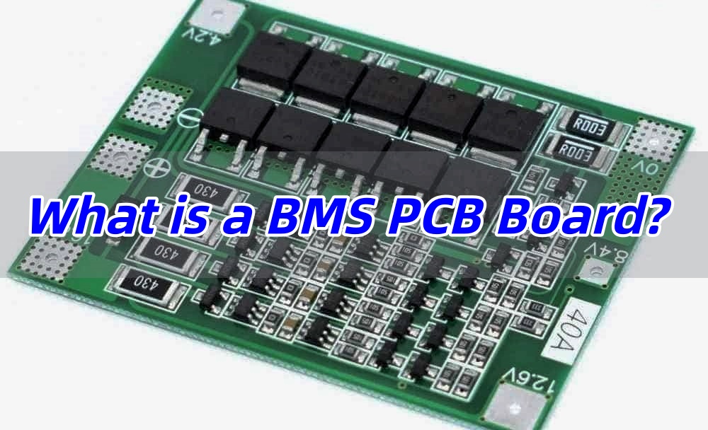
A BMS PCB board (Battery Management System Printed Circuit Board) is the essential protection and control system used in lithium battery packs, especially in 18650, Li-ion, LiPo, and LiFePOâ applications. From simple consumer electronics to EV battery packs, the BMS PCB ensures safe charging, stable discharging, cell balancing, and real-time battery monitoring.
This guide covers everything you need to know about BMS PCBsâincluding how they work, types, key functions, how to choose the right board, how to test it, and why EBest Circuit (Best Technology) is a trusted BMS PCB manufacturer.
What Is a BMS PCB Board?
A BMS PCB board is an electronic circuit board designed to monitor, protect, and balance lithium battery cells. It ensures that the battery pack stays within safe operating limits, avoiding overcharging, over-discharging, overcurrent, overheating, and short circuits.
A typical BMS PCB contains:
Protection IC
MOSFET charge/discharge control
Current shunt resistors
Temperature sensors
Balancing circuitry
Communication chips (CAN, UART, RS485, Bluetooth, etc.)
Thick-copper power traces
Thermistors and connector interfaces
Because lithium batteries are highly sensitive to voltage and current fluctuations, a BMS PCB ensures that every cell operates safely and efficiently.
Types of BMS PCB Board
BMS PCBs come in several categories based on battery type, cell configuration, communication, and protection function.
1. Based on Cell Configuration
1S BMS â single-cell lithium battery
2Sâ6S BMS â common for 18650 packs
7Sâ16S BMS â used in e-bikes, scooters
20Sâ24S and above â used in ESS and EV packs
2. Based on Balancing Method
Passive balancing BMS (energy dissipated through resistors)
Active balancing BMS (more efficient; redistributes energy between cells)
A BMS PCB board (Battery Management System PCB) is the central controller responsible for ensuring that lithium battery packs operate safely, efficiently, and reliably. Since lithium batteries are sensitive to voltage, current, temperature, and balancing differences, the BMS acts as an intelligent guardian that constantly supervises the entire pack. Its functions including:
1. Overcharge Protection
2. Over-Discharge Protection
3. Overcurrent & Short-Circuit Protection
4. Temperature Protection
5. Cell Balancing
6. Charging/Discharging Control
7. SOC/SOH Estimation (Smart BMS)
8. Communication & Data Reporting (for smart BMS)
These features make the BMS the âbrainâ of a lithium-ion battery pack.
How Does a BMS Board Work?
A BMS PCB operates by continuously monitoring voltage, current, and temperature. Here is the basic workflow:
1. Voltage Sensing
Each cellâs voltage is monitored through sense lines to prevent overcharge/over-discharge.
2. Current Measurement
A shunt resistor or Hall sensor measures current passing through the pack.
3. MOSFET Switching
The BMS activates or deactivates charging/discharging MOSFETs to protect the battery.
4. Temperature Monitoring
Sensors detect overheating and disable charging/discharging if needed.
5. Balancing Circuit
If one cell becomes higher than others, balancing resistors bleed excess charge until all cells match.
6. Control Unit (in Smart BMS)
A microcontroller processes data and communicates via CAN, UART, RS485, etc.
The result is a stable, safe, efficiently managed battery system.
What Is the Difference Between PCM and BMS?
Feature
PCM (Protection Circuit Module)
BMS (Battery Management System)
Basic Protection
✔ Overcharge / Overdischarge / Overcurrent
✔ Includes PCM features
Cell Balancing
❌ Usually none
✔ Supports balancing
Communication
❌ None
✔ CAN, UART, RS485, Bluetooth
Data Logging
❌ No
✔ SOC, SOH, temperature, cycles
Complexity
Simple
Advanced
Applications
Small electronics, 18650 packs
EVs, ESS, scooters, UPS
PCM = basic protection
BMS = complete monitoring and management system
What Is a BMS PCB Used For?
A BMS PCB is used in all lithium-ion battery applications, such as:
18650 battery packs (flashlights, e-bikes, power tools)
Electric vehicles (EV, HEV, PHEV)
Energy Storage Systems (ESS)
Solar battery systems
UPS / backup power
Drones, UAVs, robotics
Medical devices
Smart home appliances
Portable electronics
E-scooters and e-motorcycles
Any application requiring safe lithium battery operation needs a BMS PCB.
Can I Run a Lithium Battery Without a BMS?
No â it is unsafe to run a lithium-ion battery without a BMS.
Without protection, lithium batteries can experience:
Overcharging â thermal runaway, fire, explosion
Over-discharging â permanent battery damage
Overcurrent â pack overheating
Cell imbalance â capacity drop, premature aging
Using a lithium-ion battery without a BMS is highly dangerous and not recommended.
How to Choose a PCB BMS Protection Board?
Selecting the right PCB BMS protection board is crucial for safety, performance, and battery lifespan. Hereâs a detailed guide to help you choose correctly:
1. Select Based on Battery Chemistry
Different lithium chemistries have distinct voltage requirements:
Battery Type
Max Charge Voltage
Needs BMS?
Li-ion / NMC
4.20V
✔ Yes
LiPo
4.20V
✔ Yes
LiFePOâ
3.65V
✔ Yes
Using the wrong BMS for your chemistry may cause incorrect cutoff points.
2. Determine the Number of Series Cells (S Count)
A BMS must match the battery packâs series number:
Pack
BMS Needed
3S (11.1V)
3S BMS
4S (14.8V)
4S BMS
7S (24V)
7S BMS
10S (36V)
10S BMS
13S (48V)
13S BMS
16S (60V)
16S BMS
3. Choose Continuous Discharge Current Rating
BMS current rating must exceed your maximum load.
Application
Suggested Current
Power banks
3â10A
Tools / drones
20â45A
E-bikes
20â35A
E-scooters
40â60A
ESS / inverter
80â200A+
High current BMS PCBs require wide copper traces and heavy copper layers (2â10 oz).
4. Pick Balancing Type
Passive balancing â economical, good for small/medium packs
Active balancing â high efficiency, ideal for EV and solar storage
Choose based on expected lifetime and precision needed.
5. Decide Whether You Need Smart Communication
Choose Smart BMS if you need:
Real-time monitoring
CAN communication with motor controller
Bluetooth APP
RS485 for energy storage
SOC/SOH estimates
If not required, a simpler PCM or basic BMS is enough.
6. PCB Structure Requirements
For reliable high-power protection boards, a proper PCB structure is essential:
High TG material (TG â„150°C)
Thick copper (2â4 oz or higher)
Reinforced pads for MOSFETs
Wide trace routing for current paths
Good thermal dissipation design
ENIG finishing for stable bonding
EBest Circuit (Best Technology) specializes in heavy-copper PCBs designed specifically for BMS modules.
7. Safety Certifications
Depending on product category/status:
UL
CE
RoHS
IEC62133
UN38.3
Choosing a compliant BMS PCB manufacturer enable to reduce risks and improves product reliability.
How to Test the BMS PCB Board?
Testing a BMS PCB board is crucial to ensure it performs safely and reliably before being integrated into a lithium battery pack. A well-designed Battery Management System must accurately sense voltages, manage current, protect against faults, and communicate with other system components. Below are 5 essential BMS PCB testing methods, each commonly used in manufacturing and engineering validation.
This step ensures the board is physically ready for electrical testing and prevents short circuits during power-up.
2. Continuity & Insulation Test (Shorts and Opens Test)
Purpose: Verify PCB traces, vias, and components are correctly connected.
How it works:
Using a multimeter or flying-probe tester, engineers check:
Shorts between power rails
Open circuits on balancing lines
Proper grounding and isolation between channels
This test eliminates wiring errors that could cause BMS malfunction or overheating.
3. Cell Voltage Detection Accuracy Test
Purpose: Ensure the BMS measures each cellâs voltage correctly.
How it works:
A variable DC power source simulates individual battery cells. The tester adjusts voltage (e.g., 2.5V â 4.2V for Li-ion cells) and compares:
Actual input voltage
BMS measurement output (through UART/CAN/IÂČC or display)
Acceptable deviation is usually ±5â10 mV for quality BMS boards. Accurate detection is crucial for safe charging and balancing.
4. Protection Function Test (OVP, UVP, OCP, SCP)
Purpose: Confirm the BMS triggers proper protection responses.
How it works:
Engineers simulate fault conditions:
Over-voltage protection (OVP): Gradually raise simulated cell voltage until BMS disconnects charging.
Under-voltage protection (UVP): Lower cell voltage until BMS cuts off discharging.
Over-current protection (OCP): Apply load current beyond spec to check if the MOSFET shuts off.
Short-circuit protection (SCP): Momentarily create a low-resistance path to verify BMS reacts instantly.
5. Balancing Function Test (Active/Passive Balance Check)
Purpose: Verify that the BMS can equalize cell voltages.
How it works:
Setting slight voltage differences between simulated cells. The BMS should under one of below situations:
Activate resistance bleeding (passive balance)
Transfer energy between cells (active balance)
Engineers measure:
Balance current
Trigger threshold
Balance response time
Balancing tests ensure better battery lifespan and capacity utilization.
EBest Circuit (Best Technology)âs BMS PCB Manufacturing Service
EBest Circuit (Best Technology) is a professional BMS PCB board and PCB & PCBA manufacturer with over 18 years of experience, providing high-reliability battery protection boards for lithium battery companies worldwide.
Why Choose EBest Circuit (Best Technology) for BMS PCB?
✔ 2â10 oz heavy-copper BMS PCBs
✔ High-TG board materials specialized for high-current
✔ IPC Class 2 & Class 3 manufacturing
✔ SMT + through-hole assembly for BMS MOSFETs/ICs
✔ 100% functional testing
✔ Customized 1Sâ30S BMS PCB solutions for 18650, LiFePO4, NMC
Industries We Support
E-bike & scooter battery manufacturers
Energy storage system providers
Drone and UAV companies
Power tool manufacturers
Custom lithium battery pack makers
If you need BMS PCB prototype, small batch, or mass production, EBest Circuit (Best Technology) provides fast turn-around and engineering support.
FAQs
1. What type of BMS do I need for 18650 batteries?
Choose a BMS based on your pack configuration (1Sâ13S), your total continuous current (5Aâ60A for standard packs), and whether you need balancing or communication. A BMS PCB protection board for 18650 should match the battery chemistry and voltage thresholds.
2. Does BMS drain the battery?
Yes, but only slightly. A typical BMS has very low standby current (10â100 ”A), which minimally affects overall battery life. High-quality BMS PCBs have optimized low-power designs to reduce parasitic drain.
3. What is a BMS PCB board used for?
A BMS PCB board is used to protect, monitor, and manage lithium-ion battery packs. It prevents overcharge, over-discharge, overcurrent, overheating, and cell imbalance. BMS PCBs are commonly used in 18650 battery packs, e-bikes, EVs, solar systems, UPS units, drones, and portable electronics.
4. What is balancing in a BMS?
Balancing ensures all cells in a series pack maintain equal voltage. This prevents weak cells from becoming overstressed, improves efficiency, and extends battery lifespan. Balancing can be passive (bleeding excess charge) or active (redistributing charge).
5. Why is my BMS cutting off power?
Your BMS may cut off power due to:
Overcurrent
Short circuit
Over-discharge
Overcharge
High temperature
Cell voltage imbalance
6. How long does a BMS last?
A high-quality BMS PCB typically lasts 5â10 years, depending on usage, heat exposure, component quality, and environment. Industrial-grade BMS modules can last even longer.
7. What happens if a BMS fails?
If a BMS fails, the battery may overcharge, over-discharge, or overheat. This can lead to permanent cell damage or dangerous thermal runaway. Therefore, quality manufacturing and thorough testing are essential for preventing BMS failure.
Have you ever wondered why engineers talk about high frequency PCB and high speed PCBs as if theyâre completely different technologiesâeven though they both deal with signals in the GHz range? Itâs a common point of confusion, and the truth is that these two types of circuit boards serve very different purposes, even if they sometimes overlap in the same system.
Whether youâre designing RF modules, 5G antennas, or high-speed digital hardware, this article gives you the clarity you need to make the right technical decisions.
What Is a High Frequency PCB?
A high frequency PCB is a printed circuit board designed to operate at frequencies above 500 MHz, and in RF/microwave applications typically from 1 GHz to 77 GHz (and beyond). These circuits carry analog RF signals where signal integrity depends heavily on dielectric behavior, phase stability, and transmission line accuracy.
Because electromagnetic waves at these frequencies are extremely sensitive to loss, materials and PCB structures must remain consistent across the entire board.
Key characteristics of high frequency PCBs include:
Very low dielectric loss (Df †0.005 in many RF materials)
Stable dielectric constant (Dk tolerance within ±0.03)
High dimensional and thermal stability
Precise impedance-controlled transmission lines
Use of specialized laminates like Rogers, Taconic, or PTFE-based materials
High frequency PCBs are essential in RF, 5G millimeter wave, radar, satellite systems, and microwave communications.
What Is a High Speed PCB?
A high speed PCB focuses on the integrity of digital signals with fast rise/fall times (not necessarily high analog frequency). In high-speed digital design, the primary goal is to ensure that the signal transitions propagate without distortion, crosstalk, jitter, or timing failures.
High speed PCBs usually operate in the hundreds of MHz to several GHz, but the defining parameter is edge rate, not the signal frequency.
Key characteristics of high-speed PCBs:
Strong emphasis on impedance control for DDR, USB, PCIe, HDMI, and SerDes
Controlled routing for skew, timing, return path, and crosstalk
Use of PCB materials with low loss (Df 0.008â0.02) for digital integrity
Multilayer stackups optimized for reference planes, differential pairs, and power integrity
High-speed PCBs are used in servers, automotive ADAS, AI hardware, IoT devices, consumer electronics, and cloud networking systems.
High Frequency PCB vs High Speed PCB: What Are the Key Differences?
Both board types deal with fast signals, yet they solve different engineering problems. A high frequency PCB focuses on electromagnetic behavior in continuous-wave or modulated analog systems. A high speed PCB focuses on digital edges and their timing.
Both require impedance control, but HF PCBs rely heavily on material performance, while HS PCBs depend on layout and timing engineering.
What is Best Material for High Frequency PCB Design?
Material selection is very important in a PCB manufacturing. A good laminate must hold a stable dielectric constant and maintain low loss across temperature, humidity, and frequency. These attributes reduce insertion loss and stabilize impedance.
Widely used for 24 GHz and 77 GHz radar, antennas, and precision RF paths
2. Rogers RO4350B laminate
A hydrocarbon ceramic material with stable electrical performance.
Dk â 3.48
Very good loss performance for mid-GHz RF
Easier to fabricate compared with PTFE
3. PTFE-based laminates (RO5880, Taconic, etc.)
PTFE delivers ultra-low loss and excellent Dk stability.
Ideal for satellite work
Strong performance in microwave and millimeter-wave designs
4. Hybrid stackups
Some designs combine PTFE layers with FR4 or hydrocarbon layers to balance cost and RF stability. This approach reduces material expense while keeping critical layers low-loss.
High frequency PCB materials must remain stable under frequency sweep. Even small Dk drift changes phase velocity and affects filter tuning, antenna gain, and RF link range. Material planning is one of the most important steps in high frequency PCB design.
High Frequency PCB Stackup and Impedance Control
High frequency stackups require precise control over dielectric thickness, copper profile, and trace geometry.
Key stackup considerations:
Dielectric thickness tolerance ±2â3%
Low-profile copper (VLP / RTF) to minimize conductor loss
Use of microstrip, stripline, and coplanar waveguides
Wherever RF accuracy and low loss are critical, high frequency PCB materials dominate.
Why Choose EBest Circuit (Best Technology) as Your High Frequency PCB Supplier?
As a leading RF and microwave PCB manufacturer, EBest Circuit (Best Technology) provides stable production for demanding RF, 5G, and microwave applications. EBest Circuit (Best Technology) offers:
Over 17 years of RF PCB manufacturing experience
Support for Rogers, Taconic, PTFE, hydrocarbon, and hybrid stackups
High-precision impedance control ±5% or better
Ability to fabricate 1â40 layer HF multilayers
Low-profile copper and high-frequency plating capability
Advanced AOI, laser drilling, back-drill, and tight-tolerance machining
Full engineering DFM support for RF layouts
Proven reliability in defense, telecom, automotive radar, and aerospace projects
If you need RF or microwave PCB manufacturing with consistent performance, EBest Circuit (Best Technology) provides fast lead times, stable quality, and expert engineering support. Contact us get your PCB prototype right now!
FAQs
1. Is a high frequency PCB the same as an RF PCB?
Not exactly. RF PCBs are a subset of high frequency PCBs and usually refer to analog circuits under 6 GHz, while high frequency PCBs may go up to 100 GHz or more.
2. Can FR4 be used for high frequency PCB design?
FR4 can be used up to ~1 GHz, but losses become too large beyond that. Rogers or PTFE materials are recommended for low loss.
Looking for PCB manufacturer in Russia? This blog will help you understand how to choose a reliable Russian PCB manufacturer and how to evaluate their manufacturing capabilities.
The top 10 PCB manufacturer in Russia are a frequent topic of discussion among engineers and purchasing personnel, who are all looking for stable and reliable manufacturing partners. The list of top 10 Russian PCB manufacturer also provides guidance for many teams, helping them find suppliers with clear processes, transparent pricing, and consistent support for both prototyping and mass production. As more and more Russian companies develop advanced electronic products, the demand for reliable PCB suppliers continues to grow.
Top 10 PCB Manufacturer in Russia
Company Name
Advantages
Production Capability
Lead Time
Rezon IT LLC
Moscow-based, serves telecom/medical sectors, ISO certified
2-16 layer PCBs, rigid-flex PCBs, prototypes
3-7 days (mass production), 5-10 days (prototypes)
HFR Electronics
Specialized in aerospace, anti-radiation technology
4-20 layer PCBs, high-speed RF boards
7-12 days (mass production), 6-8 days (prototypes)
MicroEM Technologies
Cost-effective, industrial control focus
2-12 layer PCBs, metal-core PCBs
5-9 days (mass production), 4-6 days (prototypes)
Izhevskiy Radio Zavod (IRZ)
Defense industry qualification, strict quality control
6-24 layer PCBs, military-grade PCBs
10-15 days (mass production), 8-10 days (prototypes)
Novator JSC
Communication sector expertise, signal integrity optimization
4-18 layer PCBs, HDI boards
6-10 days (mass production), 5-7 days (prototypes)
SpecElecService
Quick prototype service, small-batch flexibility
2-10 layer PCBs, prototype manufacturing
3-5 days (mass production), 2-4 days (prototypes)
Matrix Electronics
Medical device certification, biocompatible materials
4-22 layer PCBs, rigid-flex PCBs
8-12 days (mass production), 6-9 days (prototypes)
1. Core Credentials and Certification Verification
International Standard Certifications: Prioritize manufacturers with ISO 9001 (Quality Management), IPC-A-600 (PCB Acceptability) certifications to ensure global compliance.
Industry-Specific Certifications: Look for vertical-specific accreditations like IATF 16949 (automotive), ISO 13485 (medical), or AS9100 (aerospace) for specialized projects.
Environmental Compliance: Confirm adherence to RoHS (hazardous substance restrictions), REACH (chemical management) to avoid supply chain risks.
2. Technical Capabilities and Production Transparency
Technical Parameter Transparency: Demand detailed specifications for layers, trace width/spacing, hole sizes, and impedance control to validate custom designs.
Material Traceability: Choose manufacturers providing raw material supplier details (e.g., copper foil, substrate brands) and batch traceability systems.
Engineering Support Responsiveness: Evaluate DFM (Design for Manufacturability) feedback, online quoting tools, and 24/7 technical support for seamless design-to-production transitions.
3. Quality Control and Inspection Processes
Multi-Level Inspection Systems: Prefer vendors using AOI (Automated Optical Inspection), X-RAY (microvia testing), and electrical testing (flying probe/in-circuit) to minimize defects.
Sample Validation Mechanisms: Request free samples or small-batch trials to test material performance, solder reliability, and dimensional accuracy.
Transparent Quality Reports: Obtain batch inspection reports (e.g., copper thickness uniformity, impedance matching) and reliability test data (thermal shock, moisture resistance).
4. Supply Chain and Delivery Reliability
Localized Logistics Networks: Select manufacturers with Russian warehouses or logistics partners to reduce lead times (e.g., 2â5 days for Moscow-area deliveries) and mitigate cross-border risks.
Delivery Timeline Clarity: Confirm standard lead times (e.g., 3â5 days for double-sided boards, 7â10 days for multilayer) and expedited options to avoid delays.
Packaging and Protection Standards: Ensure packaging meets ESD (electrostatic discharge), moisture, and shock protection requirements to prevent transport damage.
5. Client References and Case Studies
Third-Party Review Platforms: Check professional ratings and client feedback on platforms like Clutch or GoodFirms, focusing on repeat collaboration rates and issue resolution efficiency.
Industry Case References: Request examples of similar projects (e.g., high-frequency PCBs, HDI boards, rigid-flex designs) to verify performance in complex designs.
Local Collaboration Experience: Prioritize manufacturers with proven experience partnering with Russian enterprises, familiar with local regulations, language, and cultural norms.
6. Cost and Value Optimization
Transparent Pricing Structure: Require itemized quotes (materials, processing, testing, logistics) to avoid hidden costs and enable cost comparisons.
Long-Term Partnership Benefits: Explore volume discounts, annual framework agreements, and technical training support to optimize long-term costs.
Cost-Quality Balance: Avoid compromising quality for lower prices; validate cost-effectiveness through sample testing to ensure return on investment.
How to Evaluate the Production Capacity of PCB Manufacturer in Russia?
Monthly Average Production Area: Manufacturers must provide monthly production square footage data for various substrate types (FR-4, high-frequency, metal-based, etc.) over the past six months, specifying capacity allocation ratios between prototype lines and volume production lines.
Lamination Technology Ceiling: Confirm multi-layer board mass production capabilities, focusing on stable monthly output for 8-32 layer boards and HDI process microvia/trace width limits (e.g., 50ÎŒm/50ÎŒm).
Equipment Load Threshold: Review daily effective operating hours of key equipment (LDI exposure machines, vacuum presses, AOI inspection systems), ensuring load rates stay below 85% to maintain emergency order capacity.
2. Material Supply Chain Stability
Substrate Inventory Depth: Audit regular inventory levels for high-frequency substrates (Rogers/Taconic) and specialty substrates (aluminum-based/ceramic-based), prioritizing vendors with direct supply partnerships with renowned material brands.
Chemical Management: Require batch traceability systems for electroplating chemicals and dry film consumables, evaluating RoHS/Halogen-Free material quality control processes.
Cross-Border Material Turnover: For imported specialty materials (domestic FT-4 substrates, Japanese electrolytic copper foil), confirm average procurement lead times and emergency contingency plans.
3. Process Capability & Bottleneck Identification
Specialty Process Capacity: Quantify monthly maximum processing area for specialized processes including impedance control (±10%), blind/buried vias, and rigid-flex boards.
Prototype Conversion Rate: Analyze prototype-to-volume order conversion data, with premium vendors maintaining conversion rates of at least 35%.
Bottleneck Process Audit: Evaluate production rhythms for critical processes (immersion gold/electro-gold lines, laser drilling systems), requiring capacity improvement plans for these stations.
4. Quality Assurance System Alignment
Quality Personnel Ratio: Verify that quality department staffing constitutes at least 15% of total workforce, confirming IPQC/OQC shift coverage across all production periods.
Inspection Equipment Density: Calculate AOI/AXI equipment count per thousand square meters of capacity, assessing detection precision for 3mil line/space dimensions.
Quality Data Transparency: Review First Pass Yield (FPY) reports from recent quarters, focusing on delivery yield fluctuations for multi-layer and HDI boards.
5. Capacity Elasticity Evaluation Criteria
Expansion Response Timeframe: Understand decision-making processes for activating additional shifts or outsourcing collaboration during demand surges, with premium suppliers capable of responding within 72 hours.
Quarterly Capacity Planning: Require quarterly capacity scheduling plans, prioritizing vendors with lean production models and capacity visualization management systems.
6. Technology Evolution Compatibility
R&D Investment Ratio: Audit annual revenue allocation to new process R&D (recommended minimum 5%), tracking technology reserves in advanced areas such as mSAP processes and IC substrates.
Equipment Renewal Cycle: Review average service life of primary production equipment, prioritizing vendors with major equipment investments in the past three years.
Talent Pipeline Development: Evaluate training systems for process engineers and technicians, confirming technical follow-up capabilities in emerging fields like 5G and automotive electronics.
High Costs of Small-Batch Prototyping: Panelization Design Reduces Costs by 15%
Russian PCB clients face high per-unit costs in small-batch PCB prototyping due to material inefficiency, manual handling, and yield losses, it is critical challenges for rapid, budget-sensitive development.
EBest Circuit (Best Technology) provides the following solutions to this challenge:
Integrated Multi-Project Panelization: Consolidates diverse designs (2-12 layers, varying dimensions) onto single panels, boosting utilization by 30%+ and reducing material costs by 40% in verified cases.
Precision Routing Optimization: Achieves 0.08mm trace/space precision, increasing panel density by 25% and lowering unit-area costs by 15%. Maintains signal integrity for high-speed/high-frequency applications.
Transparent Cost Management: Provides DFM analysis and tiered pricing models, with 5-10% bulk-order savings. Full-chain cost transparency eliminates hidden fees, supported by standardized technical documentation.
Most of our customers report that optimized panelization design reduces the production costs of small-batch PCB prototypes by approximately 15% during the early development stage.
Design mismatches remain a common manufacturing challenge for Russian PCB customers, often leading to production delays and cost overruns. EBest Circuit (Best Technology) mitigates these risks with a free professional DFM (Design for Manufacturability) review service, ensuring a smooth design-to-production process, reducing lead times by over 15%, and improving the long-term reliability of PCB products.
EBest Circuit (Best Technology)’s free DFM verification service solution to address this challenge includes:
Trace and Spacing Feasibility Analysis: Verifying 0.08mm trace/spacing designs to proactively eliminate short circuit or open circuit risks.
Drill File Alignment Verification: Utilizing X-ray drilling positioning technology to ensure hole position accuracy within a 0.05mm tolerance.
Pre-production Stack-up Verification: Confirming substrate selection, copper thickness distribution, and dielectric constant matching to achieve ±5% impedance control accuracy.
Solder Mask Bridge Inspection: Automatically checking if solder mask bridge width is â„0.1mm to prevent solderability defects.
Pad-to-Hole Tolerance Assessment: Evaluating pad size and drill diameter to comply with IPC Class 2 standards.
Controlled Impedance Design Review: Integrating TDR test data to verify impedance consistency and ensure high-speed signal integrity.
Final Manufacturability: Providing a comprehensive report including risk assessment, optimization recommendations, and cost impact analysis.
Over 90% of our Russian partners reported a 25% increase in first-pass yield, a 40% reduction in lead time, and a 30% decrease in rework costs after undergoing DFM review.
Quality Consistency & Batch Variation: ISO Certified Quality System
Batch-to-batch quality variations undermine assembly yields and final device reliability. It is a critical concern for Russian PCB clients demanding predictable quality outcomes. EBest Circuit (Best Technology)âs ISO-certified quality framework minimizes these risks through structured process controls, ensuring stability across medical, automotive, aerospace, and industrial applications.
EBest Circuit (Best Technology)’s ISO certifications to industry demands:
ISO9001 Quality Management: Establishes robust process controls from design to delivery, reducing defect rates by 20%+ in verified cases.
ISO13485 for Medical Electronics: Ensures compliance with stringent medical device regulations, validating cleanroom processes for life-critical applications.
IATF16949 for Automotive Projects: Applies automotive-grade defect prevention protocols, including PPAP documentation and 100% dimensional inspection for high-reliability components.
AS9100D for Aerospace Electronics: Meets aerospace-specific requirements for radiation-hardened materials, thermal cycling resistance, and ESD protection, backed by FAI (First Article Inspection) reports.
Real feedback from Russian clients confirms that EBest Circuit (Best Technology)âs system translates to reduced rework, accelerated certifications, and predictable performance across high-stakes applications.
19-Year Production Wisdom â Decades of accumulated expertise with a proprietary error-tracking database, slashing design mistakes by 30% and reducing client rework costs.
Certified Compliance â Medical-grade certifications and IATF 16949 validation assure Russian clients in high-reliability sectors like automotive/aerospace of uncompromised quality.
Cost-Optimized Solutions â Tailored design approaches reduce PCB costs by 15-20% through material efficiency and process optimization, directly aligning with Russiaâs cost-sensitive engineering priorities.
24-Hour Rapid Prototyping â Urgent orders receive laser-fast 24-hour turnaround for prototypes, critical for Russian R&D teams accelerating time-to-market in competitive sectors like 5G/automotive.
99.2% On-Time Delivery â Proven reliability through precision logistics and production planning, eliminating delays for Russian procurement teams managing strict project timelines.
Batch-Level Full Inspection â 100% quality verification for mass production runs, backed by ISO 9001, IATF 16949, and medical-grade RoHS certifications that meet Russian/EU regulatory standards.
Elastic Scaling Capacity â Dynamic production lines adapt to Russian bulk orders or sudden spikes, supported by 72-hour emergency expansion protocols for critical projects.
Welcome to contact us if you have any request for PCB design, prototyping, mass production, assembly: sales@bestpcbs.com.
Frequently Asked Questions
Q1: What information do I need to provide before starting PCB manufacturing?
A1: To start manufacturing, you should prepare complete Gerber files, drill files, stack-up requirements, copper thickness, surface finish preference, and any impedance notes. Clear documentation helps engineers review manufacturability faster and reduces the chance of revision. Many buyers also include BOM and assembly drawings when PCBA service is required.
Q2: How do manufacturers control PCB quality during production?
A2: Quality control happens at multiple stages. Factories use AOI inspection, impedance tests, solder-mask alignment checks, plating thickness measurements, and 100% electrical testing. These steps confirm that the final boards match the original design intent. A well-structured ISO system adds further consistency across batches.
Q3: Why does PCB price vary so much among different manufacturers?
A3: Prices change due to material grade, copper weight, layer count, surface finish, panel utilization, and production equipment level. A supplier with advanced lamination lines, laser drilling, and fine etching control often handles complex boards with better stability. Buyers should compare both capability and long-term reliability, not only cost.
Q4: What factors influence PCB manufacturing lead time?
A4: Lead time depends on layer count, process difficulty, special materials, and production load. Simple 2â4 layer boards may finish in a few days, while HDI, RF laminates, and 10+ layer designs need more steps. Providing correct files and quick feedback helps shorten overall turnaround time.
Q5. How do I choose a reliable PCB manufacturer for complex designs?
A5: Look for a manufacturer with strong engineering support, stable process control, ISO certifications, multi-material experience, and clear communication habits. Review their past projects, inspect sample quality, and confirm their capability for HDI, controlled impedance, or high-frequency work. A supplier who explains risks early usually offers higher trustworthiness.
In an era of global supply chain uncertainties, us based pcb manufacturers specializing in industrial PCB manufacturing have emerged as a strategic choice for businesses across sectors. Unlike overseas suppliers, us based pcb manufacturers prioritize compliance with strict industrial standards (such as MIL-PRF and ISO 9001), ensuring that every circuit board meets the reliability requirements of critical applications. The core value of partnering with us based pcb manufacturers for local industrial PCB manufacturing lies in reduced lead times, eliminated tariff risks, and direct access to engineering supportâfactors that minimize project delays and enhance product performance. Whether youâre developing aerospace components or medical devices, collaborating with us based pcb manufacturers for your industrial PCB manufacturing needs delivers peace of mind, knowing your products are built to withstand rigorous industrial demands.
Choose Our US Based PCB Manufacturing â Solve Your Industrial PCB Manufacturing Pain Points
Tired of navigating the frustrations of offshore industrial PCB manufacturing? Our team of us based pcb manufacturers is designed to address the key challenges that hinder your projects. We offer flexible order quantities with no minimum requirements, solving the common issue of overseas suppliers refusing small-batch industrial PCB orders. Our local production eliminates import tariffs and reduces shipping times from weeks to days, cutting down on hidden costs and delays. With 30 years of expertise in industrial PCB manufacturing, our engineers provide 24/7 technical support to refine your designsâno language barriers or time zone gaps. As trusted us based pcb manufacturers, we hold UL and ISO 13485 certifications, guaranteeing compliance for medical, automotive, and aerospace applications. Skip the supply chain headaches: choose our us based pcb manufacturers and get high-quality, on-time PCBs tailored to your industrial needs.
Key Capabilities of Top US Based PCB Manufacturers
Top us based pcb manufacturers distinguish themselves through versatile capabilities that cater to diverse industrial demands. Hereâs what sets leading providers apart:
Full Range of PCB Types for Industrial Applications
From rigid FR-4 boards to flexible and rigid-flex PCBs, us based pcb manufacturers offer comprehensive solutions. We specialize in high-density interconnect (HDI) boards for compact industrial devices, aluminum-backed PCBs for thermal management in power electronics, and RF/microwave PCBs for communication equipment. Our production line handles boards up to 50 layers, supporting the complex circuitry required for industrial automation and IoT devices.
Advanced Manufacturing Technologies
Leading us based pcb manufacturers invest in state-of-the-art equipment, including automated optical inspection (AOI) systems, laser direct imaging (LDI) machines, and X-ray inspection tools. These technologies ensure precision in soldering, trace alignment, and component placementâcritical for industrial PCBs that operate in harsh environments (extreme temperatures, vibration, or chemical exposure).
How to Select Reliable US Based PCB Manufacturers
Choosing the right us based pcb manufacturers for your industrial PCB manufacturing project requires careful evaluation. Follow these actionable steps to identify a trustworthy partner:
Verify Certifications and Compliance
Reliable us based pcb manufacturers hold industry-recognized certifications: UL for safety, ISO 9001 for quality management, and AS9100 for aerospace/defense applications. Ask for documentation to confirm compliance with your industryâs specific standards (e.g., IATF 16949 for automotive, ISO 13485 for medical).
Evaluate Production Capacity and Lead Times
Inquire about minimum order quantities (MOQs), maximum production volume, and typical lead times. The best us based pcb manufacturers offer flexibilityâaccommodating both small-batch prototypes (1-100 units) and large-scale production runs (10,000+ units) with quick turnaround (1-5 days for prototypes, 2-3 weeks for mass production).
Check Customer References and Case Studies
Reputable us based pcb manufacturers will share references from industrial clients in your sector. Look for case studies that highlight successful projects, such as reducing downtime for a manufacturing plant or meeting strict deadlines for a defense contract.
Quick-Turn Prototype Services from US Based PCB Manufacturers
For industrial innovators and startups, quick-turn prototypes are make-or-break for product developmentâand us based pcb manufacturers excel in this area. Our rapid prototyping service delivers functional industrial PCB samples in 1-3 business days, allowing you to test designs, identify flaws, and iterate fast.
Materials and Specifications for Prototype PCBs
We use industry-standard materials (FR-4, Rogers 4350B, polyimide) for prototypes, ensuring consistency with mass production. You can customize trace widths, hole sizes, and surface finishes (HASL, ENIG, OSP) to match your final product requirements. As us based pcb manufacturers, we source materials locally, avoiding delays from international shipping.
Benefits of Local Quick-Turn Prototyping
Working with us based pcb manufacturers for prototypes means you can collaborate directly with engineers to resolve design issues in real time. No more waiting for overseas suppliers to respondâour team provides same-day feedback, helping you stay on schedule for product launches or investor demos.
High-Volume Production Solutions by US Based PCB Manufacturers
When your industrial product moves to scale, us based pcb manufacturers offer the stability and efficiency needed for high-volume industrial PCB manufacturing. Our automated production lines (equipped with SMT placement machines and wave soldering systems) handle 10,000+ units per run with consistent quality.
Cost Savings for Bulk Orders
As us based pcb manufacturers, we pass on economies of scale to clients: bulk orders qualify for volume discounts, and local production eliminates import tariffs and long shipping costs. We also offer inventory management services, storing excess PCBs and delivering them just-in-time to reduce your storage expenses.
Quality Control for High-Volume Runs
Every batch of industrial PCBs undergoes 100% AOI inspection and random X-ray testing to ensure zero defects. Our quality control team follows Six Sigma principles, maintaining a defect rate of less than 0.001%âa standard that many overseas suppliers canât match.
Industry-Specific PCB Solutions from US Based PCB Manufacturers
Us based pcb manufacturers understand that industrial sectors have unique requirementsâand we tailor our solutions accordingly:
Aerospace and Defense PCBs
We produce PCBs that meet MIL-PRF-55110 and AS9100 standards, with features like radiation hardening, flame retardancy, and resistance to extreme temperatures. Our aerospace clients rely on us for mission-critical components in satellites, drones, and military vehicles.
Medical Device PCBs
Compliant with ISO 13485 and FDA regulations, our medical PCBs are used in diagnostic equipment, implantable devices, and surgical tools. We prioritize biocompatibility, sterilization resistance, and low electromagnetic interference (EMI) to ensure patient safety.
Automotive Electronics PCBs
For electric vehicles (EVs) and autonomous driving systems, we manufacture PCBs that withstand high voltage, vibration, and temperature fluctuations. Our automotive PCBs meet IATF 16949 standards and support features like battery management, infotainment, and sensor integration.
Quality Certifications That Matter for US Based PCB Manufacturers
Certifications are non-negotiable for us based pcb manufacturers serving industrial clientsâthey prove our commitment to quality and compliance:
UL Certification
UL certification ensures our PCBs meet safety standards for flammability and electrical performance, a requirement for products sold in the US and Canada.
ISO 9001:2015
This certification validates our quality management system, ensuring consistent processes from design to delivery.
AS9100D
Specific to aerospace and defense, AS9100D demonstrates our ability to meet the strict quality requirements of these high-stakes industries.
ISO 13485
For medical device manufacturers, ISO 13485 certification confirms our adherence to medical industry quality standards.
Cost Factors to Consider When Working with US Based PCB Manufacturers
While us based pcb manufacturers may have slightly higher upfront costs than overseas suppliers, the total cost of ownership (TCO) is often lower. Hereâs what impacts pricing:
PCB Design Complexity
Factors like layer count (2-50+), trace density, and hole size affect production time and material usage. Our engineers can suggest design optimizations (e.g., reducing unnecessary layers) to lower costs without compromising performance.
Material Selection
Standard materials like FR-4 are more cost-effective, while specialty materials (e.g., Rogers for high-frequency applications) come at a premium. We help you balance performance needs with budget constraints.
Order Quantity and Lead Time
Small-batch orders or expedited lead times (1-2 days) may incur higher per-unit costs. Planning ahead and ordering in bulk can significantly reduce expenses.
Lead Time & Delivery Expectations for US Based PCB Manufacturers
One of the biggest advantages of us based pcb manufacturers is fast, reliable delivery:
Typical Lead Times
Prototypes: 1-3 business days (quick-turn option: 24-48 hours)
Medium-volume orders (100-1,000 units): 5-7 business days
High-volume orders (1,000+ units): 2-3 weeks
Shipping and Logistics
We partner with USPS, UPS, and FedEx for domestic delivery, with most orders arriving within 1-3 days of production completion. For urgent projects, we offer same-day shipping from our facilities in California, Texas, and Ohio. Unlike overseas suppliers, we provide real-time tracking and full transparency throughout the shipping process.
FAQ â Common Questions About US Based PCB Manufacturers
1. What types of industrial PCBs do US based pcb manufacturers produce?
Us based pcb manufacturers produce a wide range, including rigid, flexible, rigid-flex, HDI, aluminum-backed, and RF/microwave PCBs. We cater to aerospace, medical, automotive, industrial automation, and telecommunications sectors.
2. Are US based pcb manufacturers more expensive than overseas suppliers?
While upfront costs may be 10-20% higher, us based pcb manufacturers eliminate tariffs (up to 25% for Chinese imports), reduce shipping costs, and avoid delaysâlowering your total cost of ownership. The added value of quality, compliance, and technical support often justifies the difference.
3. Can US based pcb manufacturers handle small-batch prototype orders?
Yesâmost us based pcb manufacturers offer no-minimum order quantities, with quick-turn prototype services for 1-100 units. This is ideal for startups and engineers testing new designs.
4. What certifications should I look for in US based pcb manufacturers?
Prioritize UL, ISO 9001, and industry-specific certifications (AS9100 for aerospace, ISO 13485 for medical, IATF 16949 for automotive). These ensure compliance with safety and quality standards.
5. How long does it take to receive PCBs from US based pcb manufacturers?
Prototypes take 1-3 days, medium-volume orders 5-7 days, and high-volume orders 2-3 weeks. Expedited options are available for urgent projects.
6. Do US based pcb manufacturers offer design support?
Yesâour engineering team provides free design for manufacturing (DFM) reviews, helping you optimize your PCB layout for production, reduce costs, and avoid delays.
7. Are US based pcb manufacturers compliant with environmental regulations?
Absolutelyâus based pcb manufacturers follow RoHS, REACH, and California Prop 65 regulations, ensuring our PCBs are free of hazardous substances.
8. Can US based pcb manufacturers handle high-temperature or harsh-environment PCBs?
Yesâwe specialize in PCBs for extreme conditions, using materials like polyimide (flexible) and Rogers (high-temperature) to withstand temperatures ranging from -55°C to 200°C.
Customer Success Stories â Partnering with US Based PCB Manufacturers
Aerospace Startup Reduces Prototype Time by 70%
A California-based aerospace startup needed rapid prototypes for a satellite communication system. Overseas suppliers quoted 4-week lead times, but our us based pcb manufacturers team delivered functional prototypes in 48 hours. With our design support, they resolved signal interference issues and launched their product 3 months ahead of schedule.
Medical Device Company Ensures FDA Compliance
A medical device manufacturer struggled with overseas suppliers failing to meet ISO 13485 standards. They switched to our us based pcb manufacturers and received PCBs that passed FDA inspections on the first try. Our traceability system (tracking materials from sourcing to delivery) helped them maintain compliance and win a $2M contract with a hospital network.
Automotive Supplier Scales Production with Zero Defects
An EV component supplier needed high-volume PCBs for battery management systems. Our us based pcb manufacturers automated production line delivered 50,000 units with a 0% defect rate, meeting their IATF 16949 requirements. Volume discounts and just-in-time delivery reduced their costs by 15% compared to their previous overseas supplier.
For RF engineers and PCB designers tackling high-frequency projects, the rogers ro4003 laminate datasheetis an indispensable toolâone that bridges the gap between design goals and real-world performance. Whether youâre validating material compatibility or fine-tuning signal integrity, therogers ro4003 laminate datasheet packs critical details that save time, reduce reworks, and ensure your projects meet industry standards. This guide cuts through the jargon, addresses the Reddit communityâs most common frustrations, and delivers actionable insights to make the most of this top-tier high-frequency laminate.
Getting the official rogers ro4003 laminate datasheet.pdf is crucialâavoid sketchy third-party sites with outdated versions. Head straight to Rogersâ website (https://www.rogerscorp.com), navigate to âProducts > Circuit Materials > High Frequency Laminates > RO4000 Series > RO4003C,â and download from the âTechnical Documentsâ section. The latest PDF includes updated specs, processing tips, and MSDS for compliance. Save it as âRogers-RO4003-Datasheet-Official.pdfâ for easy reference, and cross-check with Rogers support if youâre confused about any section.
What is Rogers RO4003 Laminate? Key Characteristics
Material Composition & Core Advantages
Rogers RO4003 laminate is a ceramic-filled PTFE material built for high-frequency, high-speed applicationsâno surprise itâs a favorite among engineers tired of FR-4âs limitations. Its unique blend of PTFE resin and ceramic fillers delivers consistent dielectric properties, minimal signal loss, and impressive dimensional stabilityâeven in harsh environments. Unlike some specialty laminates, itâs designed to work with standard PCB manufacturing processes, so you wonât need to overhaul your workflow to use it.
Why RO4003 Stands Out for High-Frequency Applications
When frequencies climb above 2 GHz, signal degradation and impedance drift become major headachesâand thatâs where Rogers RO4003 laminateshines. With a dielectric constant (Dk) of 3.38 (at 10 GHz) and a dissipation factor (Df) of 0.0027, it outperforms FR-4 by a mile, keeping signals crisp and energy waste low. Itâs also moisture-resistant (absorbing less than 0.04% water) and thermally stable up to 280°C, making it ideal for everything from 5G antennas to automotive radar systems. For engineers who need reliability without compromise, RO4003 is the go-to choice.
Critical Technical Specifications from Rogers RO4003 Datasheet
The rogers ro4003 laminate datasheet highlights Dk and Df as make-or-break specs for high-frequency design. Dk sits at 3.38 ± 0.05 (10 GHz), staying consistent across 1 MHzâ40 GHzâso you can predict impedance matching with confidence. Df (0.0027 at 10 GHz) remains low even at elevated temperatures, a game-changer for applications like industrial sensors or outdoor communication gear. These values translate to fewer design iterations and more reliable end products.
Thermal Performance & Mechanical Properties
Thermal stability is non-negotiable for high-stress applications, and the rogers ro4003 laminate datasheet delivers: a glass transition temperature (Tg) of 280°C, well above typical operating limits. Its coefficient of thermal expansion (CTE) matches copper (17 ppm/°C in x/y direction), reducing delamination risk during soldering. Mechanically, itâs tough tooâflexural strength of 269 MPa (tensile) and 310 MPa (compressive) means it can handle the rigors of aerospace, automotive, and industrial use.
One of RO4003âs biggest perks (per the datasheet) is its compatibility with standard FR-4 workflowsâno specialized equipment needed. For drilling, use carbide drills (130â140° point angle) and slow feed rates by 20% to prevent delamination. Etch with ferric chloride or ammonium persulfate below 40°C, and plate using standard electroless copper or tin processesâjust make sure the laminate is thoroughly cleaned first. Itâs a seamless transition for PCB shops, which is why so many engineers swear by it.
Soldering & Through-Hole Treatment Best Practices
Soldering Rogers RO4003 laminate requires temperature control: the datasheet recommends 260°C for 10 seconds (per IPC/JEDEC J-STD-020). Use lead-free SAC305 solder for RoHS compliance, and preheat PCBs to 150â180°C to reduce thermal shock. For through-hole components, use a nitrogen atmosphere in reflow ovens to minimize oxidation. Avoid prolonged heat above 280°Câthis degrades the dielectric and hikes up Df, ruining performance.
Applications Where Rogers RO4003 Excels
Rogers RO4003 laminate is built for high-stakes, high-frequency applications. Top use cases include 5G base station antennas (low loss = longer coverage), automotive radar (24â77 GHz for collision avoidance), satellite communication modules (stable in extreme temps), IoT sensors (low power + compact), and medical diagnostic devices (signal integrity matters for accuracy). The rogers ro4003 laminate datasheet breaks down application-specific limitsâlike maximum power handlingâso you can design with confidence.
Rogers RO4003 vs. RO4350B: Key Differences
Reddit users often debate Rogers RO4003 vs. RO4350Bâhereâs the quick breakdown from the datasheets. RO4003 (Dk=3.38) is cost-effective, works with FR-4 processes, and excels up to 20 GHzâperfect for volume production. RO4350B (Dk=3.48) has tighter Dk tolerance (±0.04) and lower Df (0.0037), making it better for mmWave (24â40 GHz) or aerospace. RO4350B also conducts heat better (0.6 W/m·K vs. 0.5), but costs more. If youâre balancing performance and budget, RO4003 is the smarter pick for most high-frequency projects.
Hybrid Stack-Up Design (Rogers RO4003 + FR4)
Reddit is full of questions about hybrid stack-ups (RO4003 + FR4) to cut costsâand the rogers ro4003 laminate datasheet has the answers. A typical setup: RO4003 for top/bottom signal layers (high-frequency), FR4 for inner power/ground layers. Use low-CTE FR4 (e.g., Isola FR408) to match RO4003âs 17 ppm/°C, and Rogers 2929 prepreg for adhesion. Keep RO4003 layers under 10% of total stack thickness to avoid warping, and place signal layers within 0.5 mm of ground planes to reduce crosstalk. Itâs a budget-friendly way to get high-frequency performance.
Common Quality Issues & Troubleshooting Tips
Warping Prevention in Thin RO4003 Laminates
Thin RO4003 (â€0.305 mm) warps easilyâRedditâs #1 complaint. Fix it with datasheet-proven tips: use an FR-4 carrier during drilling/etching, laminate at 200â300 psi, and cool slowly (â€2°C/min). Avoid over-etching, and if warping happens, bake between steel plates at 150°C for 2 hours. These simple steps keep thin laminates flat and functional.
Reducing Signal Loss in High-GHz Applications
Above 20 GHz, signal loss creeps inâbut the datasheet has fixes. Use wider traces (â„0.2 mm), shorten trace length, and add a ground plane under signal layers. Keep RO4003 dry (pre-bake at 120°C for 4 hours if exposed to humidity) and use thinner laminates (0.203â0.406 mm) for mmWave. These tweaks keep signals strong even at high frequencies.
FAQ: Rogers RO4003 Laminate Datasheet Questions
Where can I get a reliable Rogers RO4003 laminate datasheet.pdf? Only download from Rogersâ official website (https://www.rogerscorp.com) to avoid outdated or fake versions.
What thickness is best for 5G PCBs? 0.813 mm (32 mils) is idealâbalances low loss and compact design. High-power 5G gear uses 1.524 mm.
Does RO4003 work with standard FR-4 manufacturing? Yesâminor adjustments to drilling feed rates and soldering temps (per datasheet) are all you need.
Can I mix RO4003 with FR4 in stack-ups? Absolutelyâuse low-CTE FR4 and Rogers 2929 prepreg to prevent delamination.
Whatâs RO4003âs max operating temperature? 125°C continuous, 260°C for 10 seconds (soldering).
How is RO4003 better than FR-4 for high frequencies? Lower Dk (3.38 vs. 4.4) and Df (0.0027 vs. 0.02) mean way less signal loss above 2 GHz.
How do I avoid warping thin RO4003? Use an FR-4 carrier, control lamination pressure/cooling, and avoid over-etching.
Is counterfeit RO4003 a problem? Yesâbuy from authorized distributors (Digi-Key, Mouser) and verify lot numbers with Rogers.
Where to Source Authentic Rogers RO4003 Laminate
Counterfeit RO4003 fails to meet datasheet specsâso buy from authorized distributors like Digi-Key, Mouser, or Arrow (all listed on Rogersâ site). For volume orders, contact Rogers directly for regional partners. Always check the lot number (on packaging) with Rogers support to confirm authenticity. Avoid eBay/Alibaba sellersâtheir âRO4003â often has inconsistent Dk, poor adhesion, or high water absorption, which ruins designs. Stick to trusted sources to get the real deal.
This website uses cookies to enhance your experience, remember your preferences, and help us understand how visitors use our site. You can accept all cookies, reject non-essential cookies, or manage your settings.
This website uses cookies to improve your experience while you navigate through the website. Out of these cookies, the cookies that are categorized as necessary are stored on your browser as they are essential for the working of basic functionalities of the website. We also use third-party cookies that help us analyze and understand how you use this website. These cookies will be stored in your browser only with your consent. You also have the option to opt-out of these cookies. But opting out of some of these cookies may have an effect on your browsing experience.
Necessary cookies are absolutely essential for the website to function properly. These cookies ensure basic functionalities and security features of the website, anonymously.
Cookie
Duration
Description
cookielawinfo-checkbox-analytics
11 months
This cookie is set by GDPR Cookie Consent plugin. The cookie is used to store the user consent for the cookies in the category "Analytics".
cookielawinfo-checkbox-functional
11 months
The cookie is set by GDPR cookie consent to record the user consent for the cookies in the category "Functional".
cookielawinfo-checkbox-necessary
11 months
This cookie is set by GDPR Cookie Consent plugin. The cookies is used to store the user consent for the cookies in the category "Necessary".
cookielawinfo-checkbox-others
11 months
This cookie is set by GDPR Cookie Consent plugin. The cookie is used to store the user consent for the cookies in the category "Other.
cookielawinfo-checkbox-performance
11 months
This cookie is set by GDPR Cookie Consent plugin. The cookie is used to store the user consent for the cookies in the category "Performance".
viewed_cookie_policy
11 months
The cookie is set by the GDPR Cookie Consent plugin and is used to store whether or not user has consented to the use of cookies. It does not store any personal data.
Functional cookies help to perform certain functionalities like sharing the content of the website on social media platforms, collect feedbacks, and other third-party features.
Performance cookies are used to understand and analyze the key performance indexes of the website which helps in delivering a better user experience for the visitors.
Analytical cookies are used to understand how visitors interact with the website. These cookies help provide information on metrics the number of visitors, bounce rate, traffic source, etc.
Advertisement cookies are used to provide visitors with relevant ads and marketing campaigns. These cookies track visitors across websites and collect information to provide customized ads.