When comparing electrical conductivity copper vs aluminum, copper is the better conductor. It offers higher electrical conductivity, lower resistivity, and better current-carrying performance in the same cross-sectional area. Aluminum is lighter and cost-effective, but it usually needs more conductor area to achieve similar electrical performance. For PCB bus bar, and high current PCB Assembly design, this difference can affect voltage drop, heat generation, copper thickness, and long-term reliability.
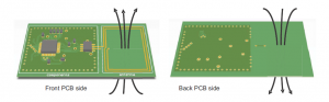
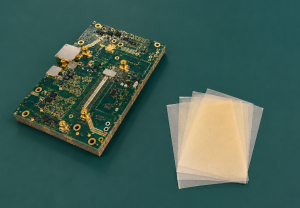
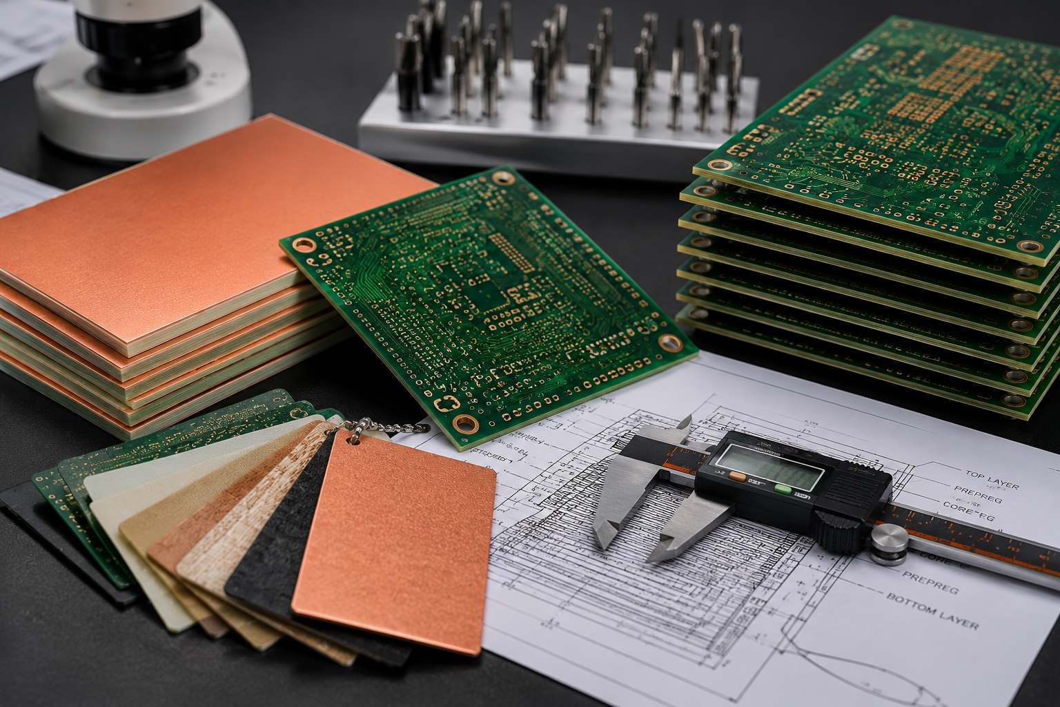
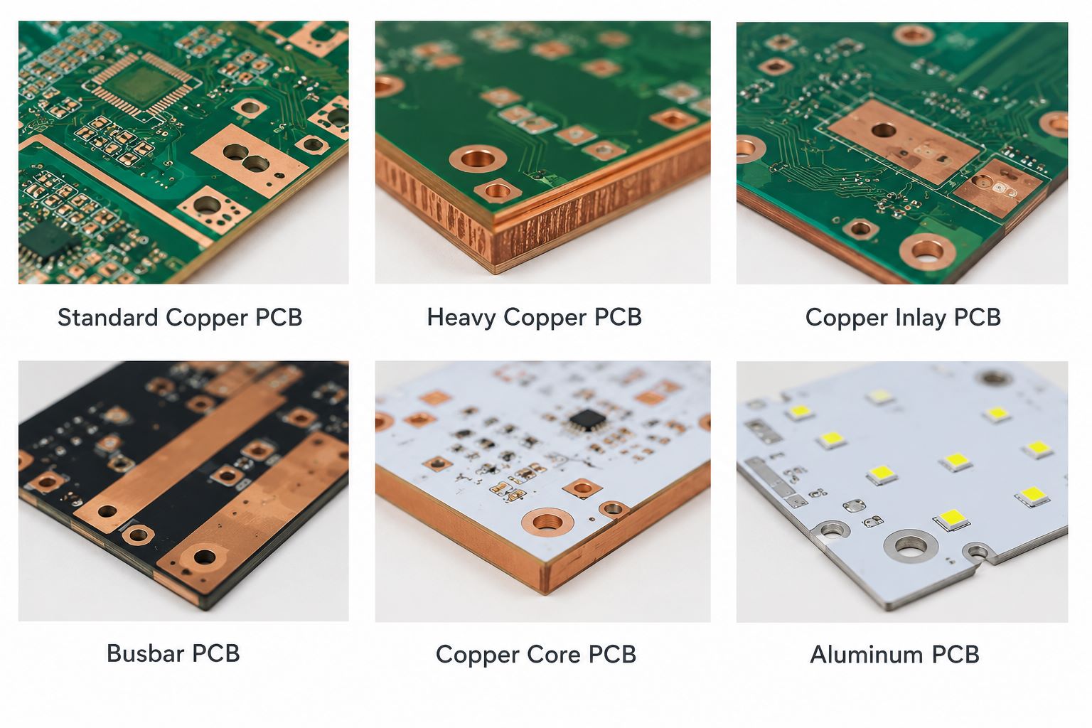
At Best Technology, we support PCB and PCBA projects where electrical conductivity, thermal management, and manufacturing reliability must work together. Our capabilities include heavy copper PCB, copper inlay PCB, busbar PCB, aluminum PCB, copper core PCB, ceramic PCB, and turnkey PCBA assembly. With ISO9001, ISO13485, IATF16949, UL, RoHS, REACH, and SGS-compliant manufacturing support, our team can help review Gerber files, BOM, current requirements, copper thickness, and thermal demands before production. For engineering support or quotation, pls feel free to send your files to sales@bestpcbs.com.
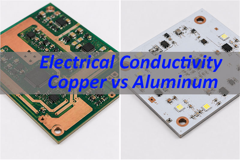
Electrical Conductivity Copper vs Aluminum: What Is the Main Difference?
The main difference is simple: copper carries current more efficiently than aluminum in the same size conductor.
Electrical conductivity describes how easily current flows through a material. Higher conductivity means lower resistance. Lower resistance helps reduce voltage drop, heat generation, and power loss.
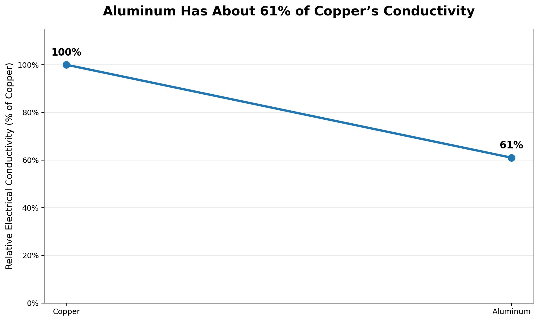
Copper is often used as the standard reference for electrical conductivity. High-purity annealed copper is rated at about 100% IACS. IACS means International Annealed Copper Standard.
Aluminum is usually around 61% IACS, depending on purity and alloy type. This means aluminum is a good conductor, but it is not as efficient as copper.
In practical design, the difference shows up in three ways:
- Copper needs less area to carry the same current.
- Aluminum needs more area to reach similar current performance.
- Copper is easier to use in compact electrical structures.
For PCB and PCBA design, space is often limited. Designers may not have enough room to make traces much wider or add large metal sections. That is why copper remains the main conductive material in most circuit boards.
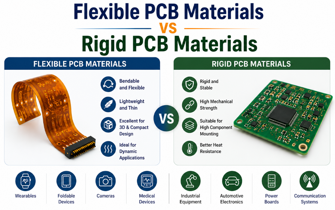
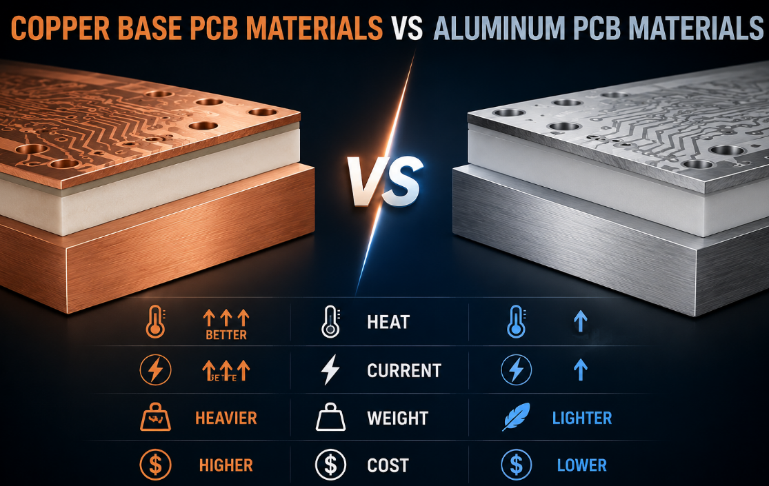
Aluminum still has value, but its role is different. In many PCB products, aluminum is used as a base material for heat dissipation, while copper still forms the circuit layer.
Copper vs Aluminum Electrical Conductivity: Key Data Comparison
A clean data table makes the comparison easier to understand.
| Material | Conductivity at 20°C | IACS Rating | Resistivity at 20°C | Density |
|---|---|---|---|---|
| Copper | About 58 MS/m | 100% | 1.68 × 10⁻⁸ Ω·m | 8.96 g/cm³ |
| Aluminum | About 35 MS/m | 61% | 2.82 × 10⁻⁸ Ω·m | 2.70 g/cm³ |
From the data, copper has better electrical conductivity. Aluminum has lower density, which means it is much lighter.
So the choice depends on the design goal.
| Design Priority | Better Choice |
|---|---|
| Higher conductivity | Copper |
| Lower resistance | Copper |
| Compact current path | Copper |
| Lower weight | Aluminum |
| Thermal base material | Aluminum |
| PCB circuit layer | Copper |
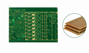
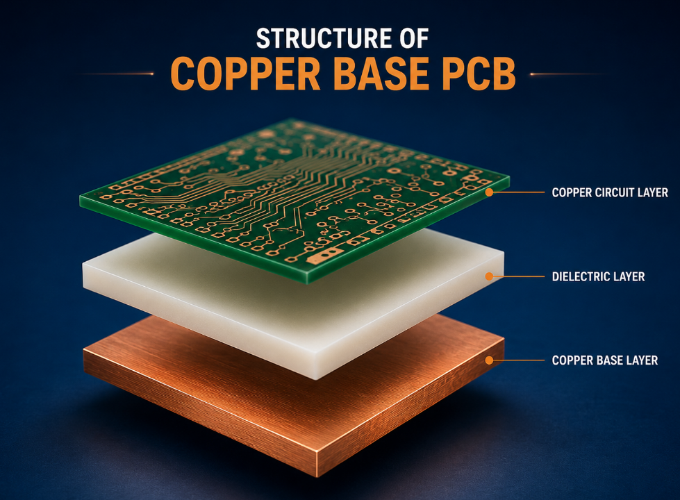
For PCB manufacturing, copper is the natural choice for electrical paths. PCB production is built around copper foil, copper plating, copper etching, copper pads, and copper vias.
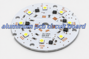
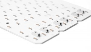
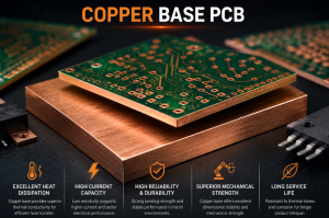
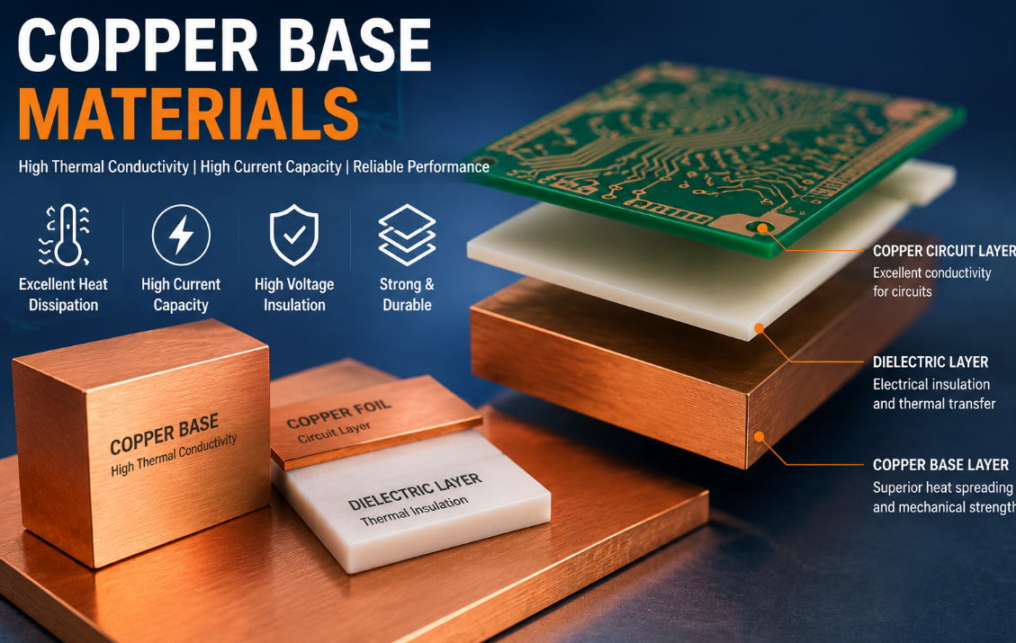
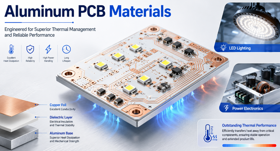
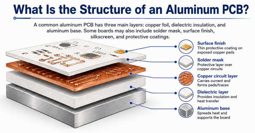
Aluminum is more common as a supporting metal base. In an aluminum PCB, the aluminum base helps move heat away from components. The electrical circuit is still usually made from copper.
This distinction is important. Aluminum PCB does not mean the circuit traces are made from aluminum. In most cases, the aluminum works as the heat-spreading base, while copper carries the electrical current.
What Percentage of Copper’s Conductivity Does Aluminum Have?
Aluminum has about 61% of copper’s electrical conductivity based on the IACS standard.
This is one of the most useful numbers when comparing aluminum vs copper electrical conductivity. It means that if copper is treated as 100%, aluminum is a little over half of copper’s conductivity.
That does not make aluminum weak. It simply means aluminum needs more conductor area to achieve similar current performance.
A short practical comparison:
| Same Design Condition | Result |
|---|---|
| Same conductor size | Copper has lower resistance |
| Same current load | Aluminum generates more resistance loss |
| Same voltage drop target | Aluminum needs more area |
| Same compact PCB space | Copper is easier to design |
| Same weight target | Aluminum may be attractive |
This is why aluminum can work well in large structures, but copper is preferred in compact electronics.
In PCB design, the available copper area is often limited by board size, spacing rules, component density, and assembly constraints. If the design needs higher current, engineers usually increase copper thickness, trace width, copper plane area, or via quantity.
For example, a high-current board may need 2 oz, 3 oz, 4 oz, or heavier copper. Some projects may require heavy copper PCB, copper inlay PCB, busbar PCB, or copper core PCB to manage both current and heat.
The key point is this: conductivity percentage is only the starting point. The final performance depends on the complete conductor structure.
What Is the Best Conductor of Electricity?
Silver is the best electrical conductor among common metals. It has slightly higher conductivity than copper. However, silver is expensive and not practical for most PCB current paths or large conductive structures.
Copper is the best practical conductor for most electronic and electrical designs. It offers an excellent balance of conductivity, cost, availability, process compatibility, solderability, and mechanical strength.
Here is a simple comparison:
| Metal | Conductivity Level | Typical Role |
|---|---|---|
| Silver | Highest | Special contacts, plating |
| Copper | Very high | PCB circuits, busbars, connectors |
| Gold | High | Contact surfaces, gold fingers |
| Aluminum | Good | Lightweight parts, metal PCB bases |
| Brass | Medium-low | Terminals, mechanical parts |
| Nickel | Low-medium | Barrier plating, protective layers |
| Stainless steel | Low | Structural and spring parts |
Gold is often seen in PCB surface finishes, but it is not used because it conducts better than copper. Gold is valued because it resists oxidation and provides stable contact performance.
In most PCBs, copper is still the real current carrier. Gold, nickel, tin, silver, or OSP surface finishes are mainly used to protect copper and support soldering or contact reliability.
This is why copper remains the most important conductive metal in PCB and PCBA production.
How Does Copper Compare to Other Metals in Electrical Conductivity?
Copper performs better than many metals used in electrical products. It has much lower resistance than brass, nickel, stainless steel, and most common alloys.
This matters because electrical resistance creates heat. When current passes through a conductor, part of the electrical energy is lost as heat. In a high-current PCB or PCBA, that heat may cause voltage drop, hot spots, solder joint stress, or long-term reliability issues.
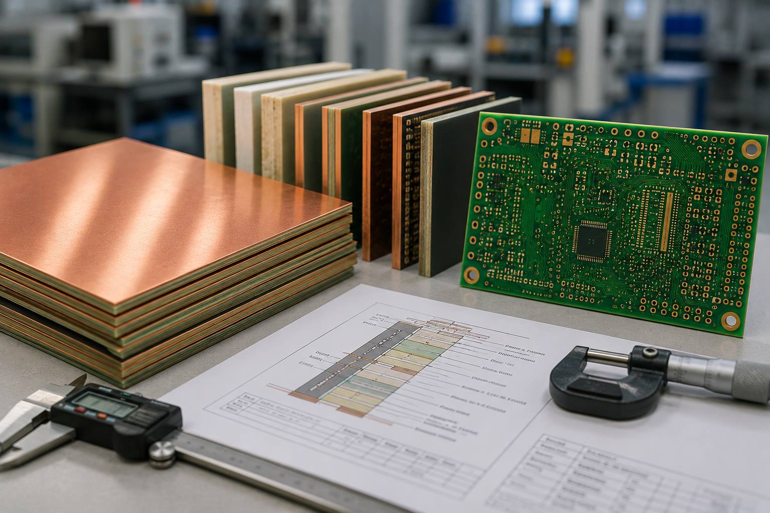
Copper also has strong process compatibility. It can be laminated, etched, plated, drilled, filled, bonded, and soldered through mature PCB manufacturing processes. That makes it suitable for standard FR4 PCB, heavy copper PCB, copper core PCB, ceramic PCB, and high-current PCBA.
Aluminum has a different advantage. It is lighter and often more cost-effective. It is also useful for heat spreading, especially in metal core PCB structures. But aluminum is not as easy to use as copper for fine circuit patterns, plated holes, and dense PCB interconnects.
In many PCB structures, copper and aluminum are not direct competitors. They work in different places.
Copper is usually used for:
- circuit traces
- pads
- vias
- copper planes
- plated through holes
- heavy copper layers
- copper inlays
- busbar structures
Aluminum is usually used for:
- metal base layers
- heat spreading structures
- lightweight mechanical support
- LED thermal management boards
So, the real design question is not only “which metal conducts better?” It is also “where will this metal be used in the board structure?”
Why Is Copper More Electrically Conductive Than Aluminum?
Copper is more electrically conductive because its atomic structure allows electrons to move more easily. In metals, electric current flows through free electrons. When electrons move with less resistance, conductivity is higher.
Copper has strong electron mobility and low resistivity. That is why it can carry current efficiently in a smaller area.
For engineers, this creates practical benefits:
- lower resistance
- lower voltage drop
- better current density
- less resistive heating
- stronger performance in compact layouts
- better suitability for PCB copper structures
Aluminum also has free electrons, so it conducts electricity well. But its resistivity is higher than copper’s. This means that, under the same size and current conditions, aluminum usually has more electrical loss.
This difference becomes more visible in high-current applications. A small resistance increase may not matter in a low-current signal circuit. But in power electronics, battery management systems, LED drivers, industrial controllers, motor control boards, or automotive electronics, the extra resistance can turn into measurable heat.
That is why copper is not only a “better conductor” in theory. It is also more practical when current, space, and reliability must be controlled at the same time.
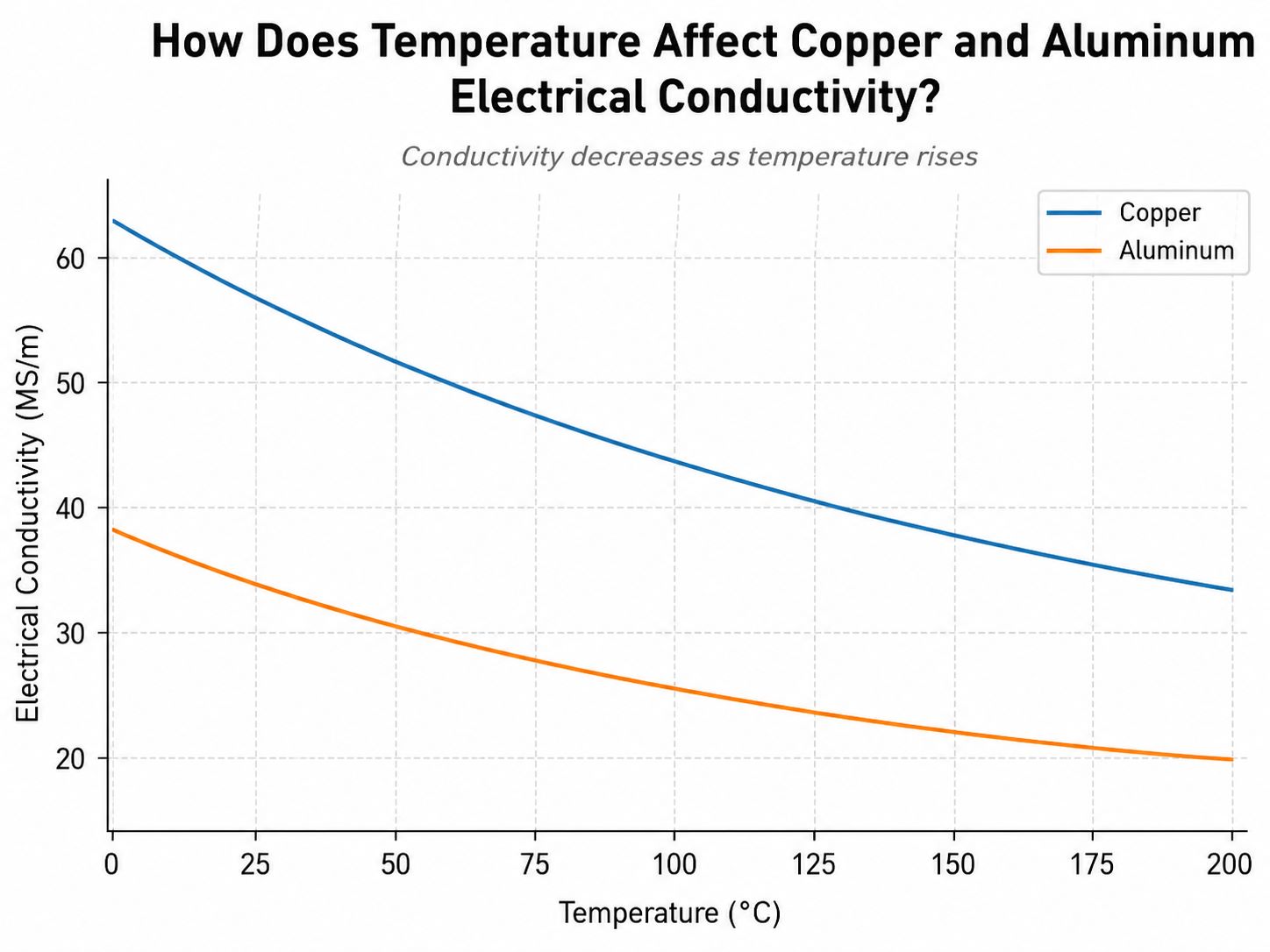
How Does Temperature Affect Copper and Aluminum Electrical Conductivity?
Temperature affects both copper and aluminum. As temperature rises, the electrical resistance of most metals increases. When resistance increases, conductivity decreases.
This is important for real products because PCB and PCBA assemblies rarely work at perfect room temperature. Many boards operate near heat-generating components, enclosed housings, LEDs, power devices, transformers, relays, MOSFETs, IGBTs, or high-current connectors.
The result is simple:
| Temperature Change | Electrical Effect |
|---|---|
| Temperature rises | Resistance increases |
| Resistance increases | Voltage drop increases |
| Voltage drop increases | Power loss increases |
| Power loss increases | Local heat may rise |
| Heat rises | Reliability margin becomes smaller |
Copper still performs better than aluminum, but copper is not immune to temperature effects. A copper path can still overheat if the trace is too narrow, the copper thickness is too thin, the via count is too low, or the current path has bottlenecks.
For high-current PCB design, engineers should consider both electrical and thermal behavior. Conductivity data at 20°C is useful, but it does not tell the full story.
A more practical review should include:
- operating current
- peak current
- copper thickness
- trace width
- via quantity
- pad size
- connector rating
- board material
- heat source location
- allowed temperature rise
- final product environment
This is where PCB manufacturing experience becomes important. A design that looks acceptable in theory may still need adjustment before production.
Is Copper or Aluminum Better for PCB, PCBA, and Busbar Design?
For PCB and PCBA current paths, copper is usually better. PCB technology is naturally based on copper. The circuit layer, plated holes, pads, vias, copper pours, and power planes are all designed around copper.
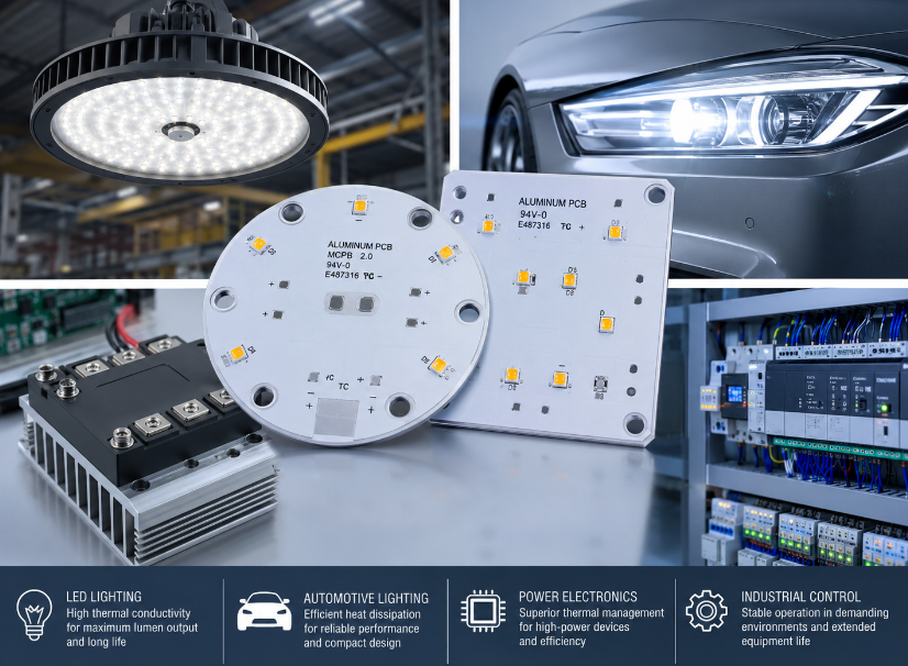
Aluminum is better when the design needs lightweight support or thermal spreading. This is why aluminum PCB is common in LED lighting, automotive lighting, power modules, and other thermal management applications.
A simple way to separate them:
| Application Need | Better Direction |
|---|---|
| PCB circuit traces | Copper |
| Plated through holes | Copper |
| High-current copper paths | Heavy copper PCB |
| Compact low-resistance path | Copper inlay PCB |
| Strong power distribution | Busbar PCB |
| LED heat dissipation | Aluminum PCB |
| Higher thermal performance | Copper core PCB |
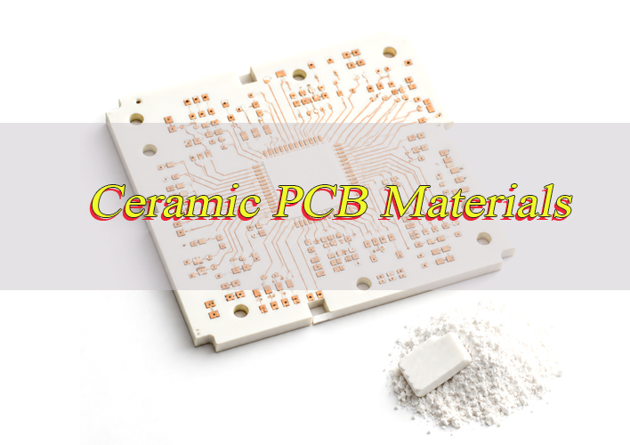
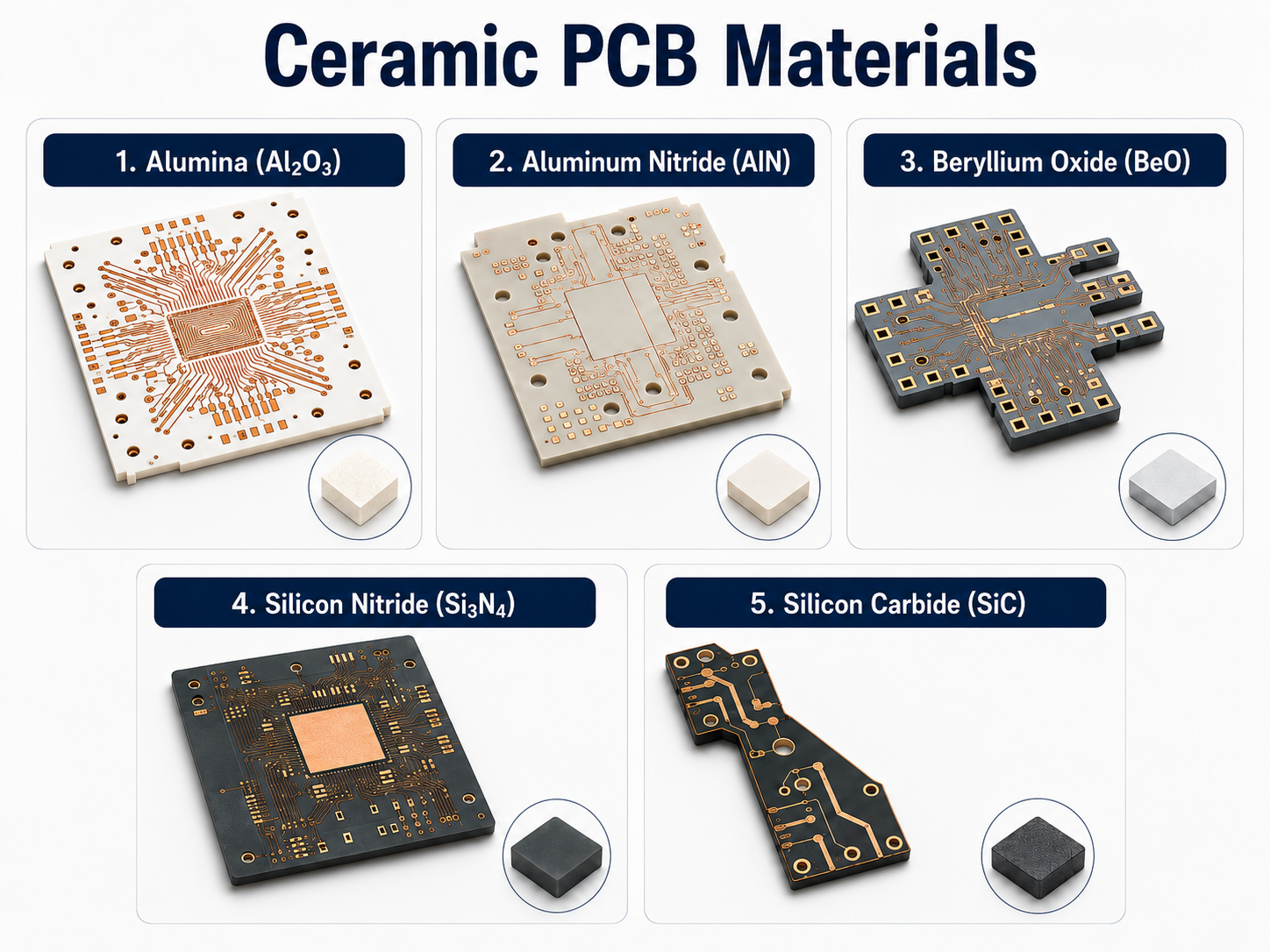
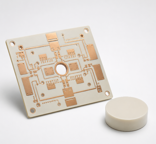
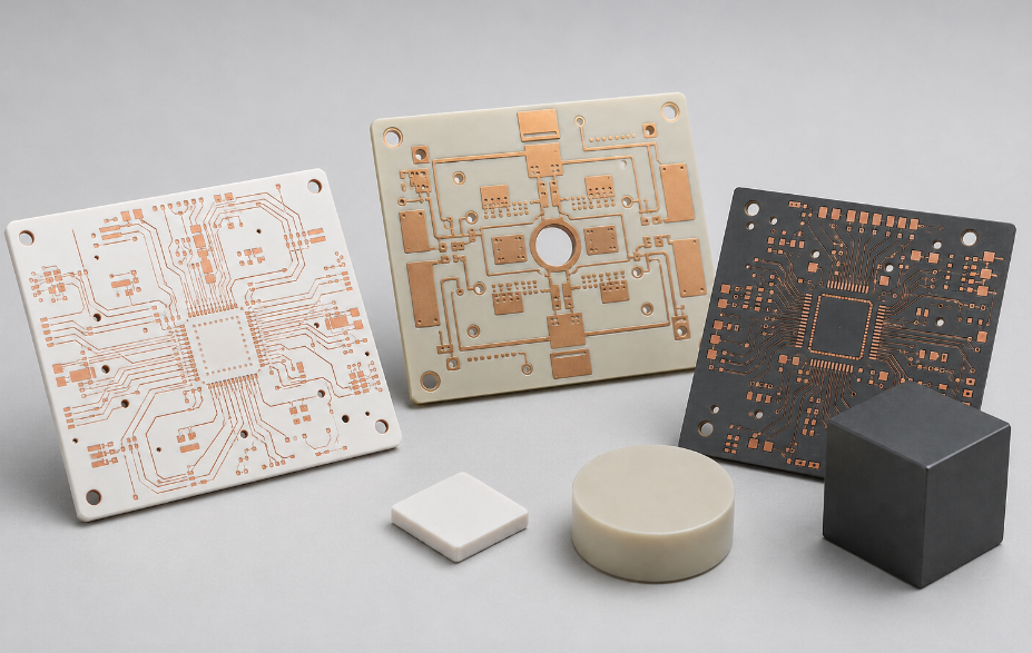
| High-power reliability | Ceramic PCB |
For busbar design, both copper and aluminum can be used. Copper busbars are more compact and conductive. Aluminum busbars are lighter and may be suitable when there is enough space.
In PCB and PCBA projects, however, copper-based structures are often easier to control. They work well with PCB fabrication, soldering, plating, and assembly processes.
The best choice depends on current, voltage drop, temperature rise, board size, insulation requirements, mechanical structure, and cost target.
A buyer should not choose only by material name. The better question is:
What board structure gives the safest electrical and thermal performance for this product?
For some projects, aluminum PCB is enough. For others, heavy copper PCB, copper inlay PCB, copper core PCB, or ceramic PCB may be more suitable.
When Should You Choose Copper Instead of Aluminum?
Choose copper when the design needs high conductivity, compact size, and stable current performance.
Copper is a better choice when your project requires:
- high current in limited space
- lower voltage drop
- better current density
- reliable soldering
- fine PCB traces
- plated through holes
- strong pad connection
- stable assembly performance
- better compatibility with PCB production
Aluminum is worth considering when weight reduction, thermal spreading, or cost control is more important than compact current carrying. It is especially useful as the metal base in aluminum PCB.
For PCB buyers, the selection can be clearer with this table:
| Project Requirement | Recommended PCB Direction |
|---|---|
| Cost-effective LED heat dissipation | Aluminum PCB |
| Higher current in limited board space | Heavy copper PCB |
| Low voltage drop and strong current path | Copper inlay PCB |
| Compact power distribution | Busbar PCB |
| Better heat transfer from power devices | Copper core PCB |
| High thermal reliability | Ceramic PCB |
| High-current assembly project | Turnkey PCBA review |
This table is not a fixed rule, but it gives a practical starting point.
For example, an LED lighting board may only need aluminum PCB if the current is moderate and the main concern is heat spreading. A motor controller may need heavy copper PCB or busbar PCB because the current path is more demanding. A high-power module may need copper core PCB or ceramic PCB if heat concentration is serious.
Before choosing the board type, buyers should prepare several key details:
| Information to Provide | Why It Matters |
|---|---|
| Operating current | Defines conductor demand |
| Peak current | Checks safety margin |
| Board size | Limits copper area |
| Copper thickness request | Affects current capacity |
| Heat source location | Supports thermal design |
| Temperature rise limit | Guides material choice |
| Gerber files | Allows layout review |
| BOM | Helps assess assembly risk |
| Application environment | Impacts reliability |
With these details, a PCB manufacturer can give more useful advice instead of only quoting a price.
FAQs About Electrical Conductivity Copper vs Aluminum
Q1: Which has better electrical conductivity, copper or aluminum?
Copper has better electrical conductivity than aluminum. Copper is about 100% IACS, while aluminum is usually around 61% IACS. This means copper can carry current more efficiently in the same conductor size.
Q2: What percentage of copper’s conductivity does aluminum have?
Aluminum has about 61% of copper’s electrical conductivity based on the IACS standard. The exact value may vary slightly depending on alloy type, purity, and temperature.
Q3: Is aluminum PCB made with aluminum circuit traces?
Usually no. In most aluminum PCB structures, the circuit layer is still copper. The aluminum layer works as the metal base for heat dissipation, especially in LED, power, and automotive applications.
Q4: Is copper better for high-current PCB design?
Yes. Copper is usually better for high-current PCB design because it has lower resistance and better current-carrying ability. Heavy copper PCB, copper inlay PCB, and busbar PCB are common options when current, voltage drop, and heat rise must be controlled.
Q5: What should I provide for a high-current PCB or PCBA quotation?
You should provide Gerber files, BOM, operating current, peak current, copper thickness requirements, board size, temperature rise limit, thermal requirements, and application environment. These details help the manufacturer review the copper structure, material choice, and assembly risks before production.
To wrap up, copper has higher electrical conductivity than aluminum, so it is usually the better choice when current flow, compact size, low resistance, and reliability are important. Aluminum remains useful because it is lightweight, cost-effective, and effective as a thermal base material.
For PCB and PCBA projects, the best material choice depends on more than one number. Copper thickness, trace width, via design, pad connection, board structure, heat dissipation, and assembly conditions all affect the final result.
Best Technology supports high-performance PCB and PCBA solutions, including aluminum PCB, heavy copper PCB, copper inlay PCB, busbar PCB, copper core PCB, ceramic PCB, and full and partial turnkey PCB assembly. If your project involves high current, LED modules, power electronics, automotive electronics, industrial control boards, or thermal management design, you can send your Gerber files, BOM, drawings, and technical requirements to sales@bestpcbs.com for an engineering review.