PCB manufacturing PCB manufacturing
Home > Blog

What Is a Start Stop Circuit and How Does It Work?

April 28th, 2026

A start stop circuit is a control circuit used to start, hold, and stop electrical equipment safely. You will often see it in motor control panels, pumps, fans, conveyors, compressors, automation machines, and industrial control systems. The basic idea is simple: press the Start button to energize the system, and press the Stop button to shut it down.

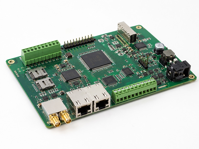
However, behind this simple action is an important control logic. A good start and stop circuit must handle electrical safety, operator control, machine protection, relay or contactor operation, overload protection, and signal reliability. For PCB and PCBA manufacturing, this type of circuit is also closely related to control board design, relay output design, terminal block layout, isolation spacing, copper thickness, soldering quality, and functional testing.
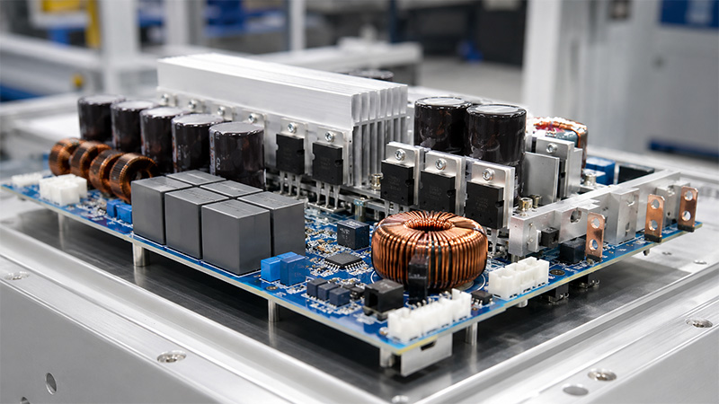
In this article, we will explain how a start stop circuit works, how different wiring methods are used, what a start stop circuit diagram should include, and how PCB design affects long-term reliability.

start stop circuit

What Is a Start Stop Circuit?

A start stop circuit is an electrical control circuit that allows a machine or device to be started and stopped using separate push buttons. It is commonly used with relays, contactors, motor starters, PLC input modules, and industrial control PCBs.

In a traditional control panel, the circuit usually includes:

PartCommon Contact TypeFunction
Start buttonNormally open, NOStarts the circuit when pressed
Stop buttonNormally closed, NCOpens the circuit when pressed
Relay or contactor coilCoil loadEnergizes the control device
Auxiliary holding contactNormally open, NOKeeps the circuit running after Start is released
Overload relayNormally closed, NCStops the motor during overload
LoadMotor, pump, fan, machineThe equipment being controlled

The most important feature is the holding circuit, also called a latching circuit or seal-in circuit. This allows the machine to keep running after the operator releases the Start button.

For example, when an operator presses Start, the contactor coil receives power. Once the contactor pulls in, an auxiliary contact closes in parallel with the Start button. That closed contact keeps current flowing to the coil. The machine continues running until the Stop button is pressed or a safety device opens the circuit.

In PCB-based control products, the same logic may be created with:

  • Mechanical relays
  • MOSFETs
  • Optocouplers
  • MCU logic
  • PLC input and output terminals
  • Solid-state relay modules
  • Power control ICs

So, a start stop circuit can be built as a classic relay-control circuit or as a modern electronic control board.

How Does a Start Stop Circuit Work?

A start stop circuit works by controlling the power path to a relay coil, contactor coil, motor starter, or electronic switching device. The circuit has two basic operating states: stopped and running.

When the system is stopped, the Start button is open, so the control coil does not receive power. The machine remains off.

When the operator presses the Start button, the button closes for a short moment. Current flows through the Stop button, overload contact, Start button, and finally into the relay or contactor coil. The coil energizes and closes its main contacts. These main contacts allow power to reach the motor or load.

At the same time, an auxiliary contact closes. This auxiliary contact is wired in parallel with the Start button. Once it closes, it creates a second path for the control current. That is why the machine keeps running after the Start button is released.

When the operator presses the Stop button, the normally closed contact opens. This breaks the control circuit. The coil loses power, the contactor opens, and the motor stops.

The logic can be summarized like this:

ActionCircuit ResultMachine Status
Start button pressedCoil energizedMachine starts
Start button releasedHolding contact keeps coil energizedMachine keeps running
Stop button pressedControl circuit opensMachine stops
Overload tripsControl circuit opensMachine stops for protection
Power loss occursCoil drops outMachine stops

This design is widely used because it supports safe manual control. After a power failure, the machine usually does not restart automatically unless the circuit is intentionally designed for that behavior. This helps protect operators and equipment.

In industrial PCBA design, the same control logic must be handled carefully. The PCB may need input filtering, surge suppression, EMI protection, and isolation between control voltage and power switching areas.

What Are the Main Components in a Start and Stop Circuit?

A start and stop circuit may look simple on paper, but each component has a clear purpose. If one part is selected incorrectly, the whole control system may become unstable.

Start push button

The Start button is normally open. It only closes when pressed. In most machines, it is green or marked with “I”. Its job is to send a temporary start signal to the control circuit.

For PCB control boards, the Start signal may come from a panel button, membrane switch, metal dome keypad, touch input, or external terminal block. The PCB input circuit should be designed to prevent false triggering caused by noise, contact bounce, or long cable interference.

Stop push button

The Stop button is normally closed. It opens when pressed. This design is preferred because it is safer. If a wire breaks, a terminal loosens, or the button fails open, the machine stops instead of continuing to run.

This is an important point for industrial control boards. Safety-related stop signals are usually designed as active-open signals rather than active-close signals.

Relay or contactor

A relay is used for smaller loads or signal switching. A contactor is used for larger motors and higher current loads. In a motor start stop circuit, the contactor usually controls the three-phase power line, while the start stop control circuit operates at a lower voltage.

For PCBA manufacturing, relays need enough PCB spacing, suitable copper width, solid solder joints, and proper mechanical support. Large relays and terminal blocks may also need wave soldering or selective soldering after SMT assembly.

Auxiliary holding contact

The auxiliary contact is what makes the circuit stay on after Start is released. It creates the latching function. Without this contact, the machine would only run while the Start button is being held down.

On an electronic control PCB, this function can also be performed by MCU firmware, a flip-flop circuit, or relay feedback logic.

Overload protection

Motor circuits often include an overload relay. If the motor draws too much current for too long, the overload relay opens its normally closed contact and stops the control circuit. This protects the motor winding and the equipment.

PCB terminal blocks and connectors

In real industrial products, the start button, stop button, limit switch, motor starter, alarm output, and power supply often connect through terminal blocks. Good PCB layout should leave enough room for wiring, labels, screw access, creepage distance, and service inspection.

What Is the Difference Between a 2 Wire and 3 Wire Start Stop Circuit?

A common search question is the difference between a 2 wire start stop circuit and a 3 wire start stop circuit. These two designs behave differently.

TypeMain FeatureCommon Use
2 wire circuitUses a maintained contact deviceSimple remote control, float switch, thermostat
3 wire circuitUses momentary Start and Stop buttons with holding contactMotor starters, industrial machines, control panels

A 2 wire circuit usually uses one maintained switch. When the switch is closed, the circuit runs. When the switch is open, the circuit stops. This is simple, but it may restart automatically after a power failure if the switch remains closed.

A 3 wire start stop circuit uses three control paths: Stop, Start, and holding contact. The Start button is momentary. The Stop button is normally closed. The auxiliary contact holds the circuit after starting.

The 3 wire method is preferred for many motor control systems because it gives better operator control. After power is lost, the circuit drops out. The operator usually needs to press Start again after power returns. This reduces unexpected restart risk.

A simplified 3 wire logic looks like this:

Power → Stop NC → Overload NC → Start NO → Coil → Neutral
                         │
                         └── Auxiliary NO Holding Contact ──┘

When the coil energizes, the auxiliary contact closes. That contact bypasses the Start button and keeps the coil active.

For PCB and PCBA design, the 3 wire logic can be implemented with external wiring or integrated into the control board. If the board handles the latching logic electronically, engineers must define what happens during power loss, brownout, emergency stop, reset, and fault recovery.

This is where manufacturing experience matters. A PCB used in industrial control should not only match the schematic. It should also support stable field operation.

How Does a Motor Start Stop Circuit Control Industrial Equipment?

A motor start stop circuit controls the motor by energizing or de-energizing a motor contactor. The control circuit does not usually carry the full motor current. Instead, it controls the coil of the contactor. The contactor then switches the higher-power motor line.

For a 3 phase motor start stop circuit, the power section usually includes:

  • Three-phase input power
  • Main breaker or fuse
  • Magnetic contactor
  • Thermal overload relay
  • Three-phase motor

The control section usually includes:

  • Stop button
  • Start button
  • Contactor coil
  • Auxiliary holding contact
  • Overload relay auxiliary contact
  • Indicator lamp
  • Optional emergency stop
  • Optional PLC signal

This structure is used in many industrial applications:

ApplicationStart Stop Circuit Function
Conveyor systemStarts and stops material movement
Pump controllerControls water, oil, or chemical pumping
Ventilation fanControls airflow in equipment rooms
CompressorControls motor operation and protection
Packaging machineManages operator start and emergency stop logic
CNC auxiliary equipmentControls coolant pumps, fans, and fixtures

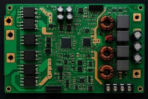
In modern equipment, the start stop function may be part of a PCBA control module. The board may include low-voltage control input, relay output, current sensing, LED indicators, and communication interfaces.

For this kind of board, PCB manufacturing quality is directly related to equipment reliability. Poor soldering, weak relay joints, narrow copper traces, or insufficient spacing can cause field failures. A control board may pass a simple power-on test, but it also needs to survive vibration, heat, repeated switching, and electrical noise.
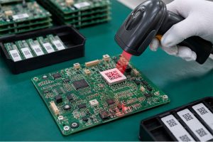
That is why an experienced PCB and PCBA manufacturer should review the design before production. DFM checks, component verification, solder joint inspection, and functional testing can reduce many hidden risks before the boards are shipped.

What Should a Start Stop Circuit Diagram Include?

A good start stop circuit diagram should be easy to read, safe to wire, and clear enough for troubleshooting. It should not only show buttons and coils. It should show the real control logic and protection path.

A proper start stop circuit schematic or drawing should include:

Diagram ItemWhy It Matters
Power sourceShows control voltage, such as 24VDC, 110VAC, or 220VAC
Stop button contact typeConfirms NC safety logic
Start button contact typeConfirms NO start logic
Relay or contactor coil ratingPrevents wrong voltage selection
Auxiliary holding contactShows latching path
Overload relay contactShows motor protection path
Emergency stopShows safety stop function
Terminal numbersHelps assembly and field wiring
Wire labelsSupports maintenance and troubleshooting
Indicator lampsShows run, stop, or fault status
Grounding and isolation notesImproves safety and EMC performance

For PCB production, the schematic should also match the PCB layout and BOM. If a circuit uses relays, terminal blocks, optocouplers, fuses, MOVs, TVS diodes, or current sensors, these parts must be clearly specified.

One common problem in control PCB projects is that the schematic looks correct, but the layout is not robust enough. For example:

  • Relay contact spacing is too small.
  • High-voltage and low-voltage areas are too close.
  • Copper width is not enough for load current.
  • Terminal blocks are too close to tall components.
  • Silkscreen labels are unclear.
  • Surge protection is missing near field wiring.
  • Screw terminal solder pads do not have enough mechanical strength.

A professional PCBA manufacturer can help check these points before mass production. This is especially useful for industrial control boards, motor control boards, power control modules, and equipment interface boards.

How Does PCB Design Affect Start Stop Circuit Safety and Reliability?

PCB design has a strong influence on the safety and reliability of a start stop control board. Even when the circuit logic is correct, weak PCB design can cause heating, arcing, noise problems, relay failure, or unstable operation.

Copper thickness and trace width

If the PCB carries relay contact current or load current, the copper width must match the actual current. Higher current may require wider traces, heavier copper, or reinforced copper areas. For motor-related control boards, inrush current and switching current should also be considered.

Creepage and clearance distance

Start stop circuits may involve different voltage areas. For example, a board may have 24VDC logic and 220VAC relay output on the same PCB. The spacing between these areas must follow safety requirements. Slots, isolation gaps, and clear silkscreen marking can improve safety.
Relay and contactor interface design

Relay coils can create voltage spikes when switched off. A good PCB design may use flyback diodes, RC snubbers, MOVs, or TVS protection depending on whether the coil is DC or AC. This protects the control circuit and improves switching life.

Input signal stability

Start and Stop buttons may connect through long wires. Long wires can pick up electrical noise in industrial environments. Input filtering, pull-up or pull-down resistors, optocoupler isolation, and debounce design help the board read signals correctly.
Thermal management

Relays, power resistors, regulators, and protection devices generate heat. Component placement should allow heat to spread. In higher-power applications, copper pours, thermal vias, and proper enclosure airflow are useful.
Mechanical strength

Industrial control boards often use screw terminals, large relays, connectors, and manual wiring. These components receive mechanical stress during installation. Larger pads, through-hole plating quality, and proper soldering processes are important.

Manufacturing test points

A well-designed PCBA should include test points for power input, ground, relay coil signal, MCU reset, button input, and output status. This makes ICT, flying probe testing, and functional testing more efficient.

From a manufacturing viewpoint, the best design is not only electrically correct. It is also easy to assemble, inspect, test, and maintain.

What Testing Is Needed for Start Stop Circuit PCBA?

Testing is essential for start stop circuit boards because they are often used in equipment where stable operation matters. A small fault can stop a machine, damage a motor, or create downtime for the user.

For PCB and PCBA production, testing may include several stages.

Bare PCB inspection

Before assembly, the bare PCB should be checked for open circuits, short circuits, hole quality, solder mask quality, copper thickness, and surface finish. For control boards with high-voltage areas, spacing and routing should also be inspected.

SMT and DIP assembly inspection

After assembly, AOI can check component placement, polarity, solder bridges, missing parts, and wrong orientation. For through-hole relays and terminal blocks, visual inspection and solder joint inspection are also important.

Relay output testing

If the board includes relay outputs, each relay should be switched during testing. The test should confirm coil operation, contact continuity, LED indication, and output terminal behavior.

Button input testing

Start, Stop, Reset, Emergency Stop, limit switch, and sensor inputs should be tested under real signal conditions. For boards with optocoupler inputs, the input voltage range should be confirmed.

Functional testing

Functional testing checks whether the board behaves as expected. For example:

  • Apply control power.
  • Confirm the board remains in Stop state.
  • Trigger the Start input.
  • Confirm relay output turns on.
  • Release Start.
  • Confirm latch or run state remains active.
  • Trigger Stop input.
  • Confirm relay output turns off.
  • Simulate overload or fault input.
  • Confirm safe shutdown behavior.

Burn-in or aging test

Some industrial control boards benefit from burn-in testing. The board runs for a defined time under voltage and load conditions. This helps reveal early component or soldering problems.

Traceability check

For industrial, medical, automotive, and high-reliability projects, material traceability matters. Batch records, component sources, inspection data, and testing records help customers manage quality over the product lifecycle.

At EBest Circuit (Best Technology), we can support PCB fabrication, component sourcing, SMT assembly, DIP assembly, relay soldering, functional testing, and box-build related support for control board projects.

How to Choose a Reliable PCB and PCBA Manufacturer for Start Stop Circuits?

Choosing the right PCB and PCBA manufacturer is important when your start stop circuit is used in industrial control, motor control, automation equipment, or power switching products. These boards need more than basic assembly. They need engineering review and process control.

A reliable manufacturer should understand both PCB production and circuit application requirements.

Here are several points to check:

Selection PointWhy It Helps
PCB fabrication capabilitySupports proper copper thickness, spacing, drilling, and surface finish
PCBA assembly experienceHandles SMT, DIP, relays, connectors, and terminal blocks
Engineering DFM reviewFinds layout, soldering, spacing, and manufacturability issues early
Component sourcing supportReduces counterfeit risk and improves BOM stability
Functional testing abilityConfirms the circuit works before shipment
Traceability systemSupports batch control and quality records
Industrial control experienceHelps with relay boards, motor control boards, and equipment PCBA
Flexible productionSupports prototypes, small batches, and mass production

For start stop circuit boards, it is helpful to work with a manufacturer that can review practical details, such as:

  • Are the relay contacts rated correctly?
  • Is the control input protected from noise?
  • Is the spacing enough for the voltage?
  • Are terminal blocks easy to wire?
  • Can the board pass functional testing?
  • Are high-current traces wide enough?
  • Are through-hole components soldered reliably?
  • Can replacement components be sourced safely?

EBest Circuit (Best Technology) provides one-stop PCB and PCBA manufacturing services for industrial control boards, power control boards, relay boards, motor control PCBs, automation equipment boards, and custom electronic assemblies. Our team can support PCB fabrication, component sourcing, assembly, inspection, and testing, helping customers move from prototype to stable production with better confidence.

If your project includes a start stop circuit, motor control board, relay control module, or industrial PCBA, you can send your schematic, Gerber files, BOM, and testing requirements for engineering review. If any questions, pls feel free to contact us via sales@bestpcbs.com.

To sum up, a start stop circuit is one of the most widely used control circuits in electrical and industrial systems. It allows operators to start equipment, keep it running through a holding contact, and stop it safely when needed. Although the working principle is simple, the real design requires careful attention to wiring logic, contact ratings, overload protection, PCB layout, isolation spacing, and functional testing.

For PCB and PCBA projects, start stop circuits often appear in motor control boards, relay modules, automation controllers, power control boards, and industrial equipment interfaces. A reliable board should be easy to wire, stable in noisy environments, safe under voltage stress, and tested before delivery.

Working with an experienced PCB and PCBA manufacturer helps reduce design risk and improve production quality. From DFM review to component sourcing, assembly, inspection, and functional testing, every step contributes to a more dependable control board.

FAQs About Start Stop Circuit

What is a start stop circuit used for?
A start stop circuit is used to control equipment startup and shutdown. It is common in motors, pumps, fans, conveyors, machine tools, and industrial automation systems.

What is a 3 wire start stop circuit?
A 3 wire start stop circuit uses a Stop button, Start button, and auxiliary holding contact. It allows the machine to keep running after the Start button is released.

Why is the Stop button normally closed?
The Stop button is normally closed for safety. If the wire breaks or the button fails open, the control circuit opens and the machine stops.

What is the difference between a start stop circuit and a latching circuit?
A latching circuit keeps its output active after a temporary input signal. A start stop circuit often uses latching logic to keep a motor or relay running after the Start button is released.

Can a start stop circuit be built on a PCB?
Yes. A start stop function can be built on a PCB using relays, transistors, MOSFETs, optocouplers, MCU logic, or PLC interface circuits.

What should be checked before producing a start stop circuit PCBA?
The manufacturer should check schematic logic, PCB spacing, copper width, relay rating, terminal layout, component availability, soldering process, and functional test requirements.

What is a motor start stop circuit?
A motor start stop circuit controls a motor contactor. The control circuit energizes or de-energizes the contactor coil, and the contactor switches motor power.

Why does PCB quality matter in start stop circuits?
PCB quality affects electrical safety, solder joint strength, relay performance, signal stability, and long-term reliability in industrial environments.

You may also like

What Are Circuit Boards Applications Uses in Electronic Devices?

April 21st, 2026

Circuit boards applications uses electronics devices refers to how Printed Circuit Boards support, connect, and control the functions of modern electronic products across consumer, industrial, medical, automotive, and other advanced sectors. This article explains where PCBs are used, how they work, which board types and materials fit different scenarios, and how to choose the right PCB partner for reliable results.

What problems do customers usually face when selecting PCBs for electronic devices?

  • The device works in theory, but the PCB fails in real operating conditions.
  • The board is too bulky for compact product design.
  • Heat, moisture, or vibration shortens product life.
  • Material choice is unclear, especially for RF, power, or harsh environments.
  • A supplier can build boards, but cannot support application-driven optimization.

A capable PCB manufacturer solves these issues by matching the board to the real application environment.

  • Use application-specific PCB structures and stackups.
  • Reduce board size through HDI and optimized layout support.
  • Improve durability with thermal and environmental design controls.
  • Recommend the right substrate for signal, power, and reliability needs.
  • Provide engineering support from DFM review to mass production.

EBest Circuit (Best Technology) is a professional PCB and PCBA manufacturer serving customers across consumer electronics, industrial control, medical devices, automotive electronics, RF products, LED systems, and high-reliability applications. We support projects with engineering review, material selection, PCB fabrication, component sourcing, SMT assembly, testing, and fast communication throughout the process. For project support, pls feel free to contact us via sales@bestpcbs.com.

Circuit Boards Applications Uses Electronics Devices

What Are Circuit Boards Applications Uses in Electronic Devices?

When people search for Applications of circuit boards in electronic devices or Circuit board applications in electronics, they are usually asking a practical question: where are PCBs used, and what do they actually do inside a product? A PCB is not just a mounting platform. It is the electrical foundation that links components, manages signals, distributes power, and helps a device operate as one complete system.

At the application level, PCBs serve several core functions:

  • Electrical connection: link ICs, resistors, capacitors, connectors, and sensors
  • Signal routing: guide analog, digital, RF, and high-speed signals through controlled paths
  • Power distribution: deliver stable voltage and current to all functional blocks
  • Mechanical support: hold components in fixed positions for reliable assembly
  • Thermal assistance: help move heat away from power devices and LEDs
  • System integration: combine control, sensing, communication, and power modules on one board

A quick application view looks like this:

PCB RoleWhat It Does in a Device
ConnectionLinks all electronic parts
ControlSupports processing and logic
PowerFeeds current to subsystems
CommunicationCarries data and RF signals
Thermal supportHelps reduce hot spots
StructureSupports assembly and compact design

In short, circuit boards uses applications electronics devices is really about how PCBs make modern electronics possible. Without them, devices would be larger, less reliable, harder to manufacture, and far more expensive to integrate.

Why Are Circuit Boards Essential in Modern Electronic Devices?

Modern electronics demand more than simple connectivity. Devices now combine processors, wireless modules, displays, sensors, batteries, cameras, and power circuits in very limited space. PCBs are essential because they organize this complexity into a manufacturable, repeatable, and scalable platform.

Their importance becomes even clearer when products must meet commercial targets such as lower size, faster speed, stable performance, and long service life. A good PCB design improves both engineering performance and business outcomes.

Key reasons PCBs are essential include:

  • They enable compact integration
    Multilayer PCBs allow many circuits to fit into a small area.
  • They improve electrical consistency
    Controlled traces and reference planes help stabilize signal behavior.
  • They support mass production
    Standardized fabrication and assembly make large-scale manufacturing possible.
  • They increase product reliability
    Well-designed PCBs reduce loose wiring, assembly errors, and connection failure.
  • They help optimize cost
    Integrating more functions into one board can reduce cable, connector, and labor costs.
  • They support modern interfaces
    Bluetooth, Wi-Fi, GPS, USB, CAN, Ethernet, and RF systems all rely on PCB design quality.

For many products, PCB quality directly affects user experience. A smartphone with poor board design may overheat. A medical monitor with unstable signal routing may lose data accuracy. An automotive controller with weak vibration resistance may fail early.

So when discussing circuit board applications in electronics, the real point is not only where the board is used, but why it is indispensable to modern product architecture.

What Types of Electronic Devices Use Circuit Boards Today?

PCBs appear in almost every category of electronic equipment. Some devices use a basic single-sided board. Others rely on complex HDI, rigid-flex, RF, ceramic, or metal-core designs. The device category usually determines the PCB structure, material system, thermal requirement, and assembly complexity.

Here are the main device groups using PCBs today:

  • Consumer electronics: smartphones, tablets, laptops, smartwatches, TVs, headphones
  • Home appliances: refrigerators, washing machines, coffee makers, air conditioners
  • Industrial equipment: PLCs, drives, inverters, HMI panels, robotic controls
  • Medical devices: monitoring systems, imaging units, infusion pumps, portable diagnostics
  • Automotive electronics: ECUs, lighting modules, BMS units, infotainment systems, sensors
  • Telecom and RF devices: routers, base stations, antenna units, GPS modules
  • Security devices: cameras, alarm systems, smart locks, motion sensors
  • Energy systems: solar inverters, battery storage controllers, smart meters, charging systems

A simple way to view this is by application demand:

Device TypeTypical PCB Need
SmartphoneHDI, multilayer, compact layout
LED lightThermal management, MCPCB
Automotive ECUHigh reliability, vibration resistance
Medical monitorStable signals, compliance support
Router / RF unitControlled impedance, low-loss material
Industrial controllerDurability, long service life

This wide adoption explains why Applications of circuit boards in electronic devices is such a strong topic. It covers both daily-use electronics and critical systems that must operate under far more demanding conditions.

What Are the Most Common Circuit Board Applications in Electronics?

Although PCBs are used almost everywhere, certain applications appear far more often in search behavior and purchasing demand. These common uses create the best bridge between SEO traffic and practical buyer intent.

The most common PCB applications in electronics include the following:

Signal control boards
Used in logic control, processing, and communication modules.

Power conversion boards
Used in chargers, power supplies, inverters, and motor drives.

Interface boards
Used for display control, user input, connectors, and external communication.

Sensor boards
Used in wearables, automotive systems, industrial monitoring, and IoT products.

RF and wireless boards
Used in Bluetooth, Wi-Fi, GPS, and antenna-linked systems.

LED and lighting boards
Used in home lighting, automotive lights, indicators, and medical illumination.

Embedded controller boards
Used in smart appliances, industrial machines, and automotive modules.

A compact comparison is helpful here:

ApplicationTypical Product Examples
Signal processingPhones, tablets, computers
Power managementChargers, inverters, adapters
SensingSmartwatches, industrial meters
Wireless communicationRouters, GPS units, IoT modules
LightingLED lamps, dashboard lighting
Automation controlPLCs, robotic controllers

These are the everyday realities behind circuit boards applications uses electronics devices. The board may be hidden, but its role is central in nearly every function the user sees.

In summary, the most common applications combine control, power, communication, sensing, and interface management. That is why PCB demand remains broad across nearly all electronics markets.

How Do Circuit Boards Function Inside Electronic Devices?

Inside an electronic device, a PCB works as a coordinated electrical platform. It does not “think” by itself, but it allows processors, memory, sensors, connectors, and power devices to exchange energy and information in a controlled way.

A PCB functions through several structural elements:

  • Copper traces carry electrical signals and current
  • Pads create solderable connection points for components
  • Vias connect different copper layers
  • Planes provide stable ground and power reference areas
  • Solder mask protects copper and controls solder bridging
  • Silkscreen supports identification and assembly
  • Substrate provides insulation and mechanical strength

A simplified function path inside a device often follows this logic:

  • Power enters the board through a connector or battery terminal.
  • Power circuits regulate voltage for each subsystem.
  • A controller or processor receives input data.
  • Signals move through traces to memory, sensors, or output modules.
  • The board sends commands to motors, displays, communication chips, or LEDs.

For high-speed or RF devices, PCB function also depends on electrical design rules such as:

  • controlled impedance
  • return path continuity
  • trace length balance
  • isolation between noise-sensitive circuits
  • reference plane integrity

A commonly used signal principle is:

This reminds designers that transmission line impedance depends on inductance and capacitance per unit length. In practical PCB design, trace width, dielectric thickness, and material properties all affect signal quality.

So, in real product operation, a PCB is the controlled environment that allows electronic components to behave correctly, safely, and repeatedly.

What Types of Circuit Boards Are Used in Different Applications?

Different applications need different board structures. A low-cost toy and a medical control unit should not use the same PCB strategy. The board type must fit the device’s electrical, thermal, mechanical, and cost requirements.

The most common PCB types include:

Single-sided PCB
Used in simple, low-cost electronics with limited circuitry.

Double-sided PCB
Used where moderate circuit density is required.

Multilayer PCB
Used in smartphones, computers, telecom, and industrial controls with complex routing needs.

HDI PCB
Used in compact, high-performance devices that need fine lines, microvias, and dense interconnection.

Flexible PCB
Used where bending, folding, or space-saving interconnect is required.

Rigid-flex PCB
Used in medical, military, aerospace, and premium compact devices.

Metal Core PCB
Used mainly in LED and power applications for better heat transfer.

A selection summary:

PCB TypeBest Fit
Single-sidedBasic consumer products
Double-sidedGeneral electronics control
MultilayerComputing, telecom, industrial
HDISmartphones, wearables
FlexCameras, foldable interconnect
Rigid-flexMedical, aerospace, compact systems
MCPCBLED, power modules

Choosing the correct board type improves not only function, but also assembly yield, product lifetime, and cost efficiency. That is why board type selection should always follow actual application conditions, not habit alone.

What Materials Are Used in Circuit Boards for Different Applications?

PCB material selection has a direct impact on electrical performance, thermal stability, durability, manufacturability, and cost. Many buyers begin with FR4, but not every application should stay there.

The most common PCB materials are:

  • FR4: the standard choice for general electronics
  • High-Tg FR4: better for higher thermal stress and lead-free assembly
  • Aluminum base: strong heat transfer for LED and power boards
  • Copper base: excellent heat spreading for demanding thermal designs
  • Rogers / PTFE materials: used in RF and microwave circuits
  • Ceramic substrates: used in high-temperature, high-power, or high-reliability electronics
  • Polyimide: common in flexible and rigid-flex PCB construction

Material comparison:

MaterialTypical Use
FR4General electronics
High-Tg FR4Industrial and automotive control
AluminumLED lighting, power modules
RogersRF, antenna, microwave
CeramicPower, aerospace, high-heat environments
PolyimideFlex and rigid-flex boards

Two important parameters often influence material choice:

  • Dielectric constant (Dk): affects signal speed and impedance
  • Thermal conductivity: affects heat transfer ability

For example, an RF design may prioritize low and stable Dk. An LED board may prioritize thermal conductivity. A compact wearable may prioritize thin profile and flex endurance.

In short, materials should be selected by application physics, not by default preference. That is one of the most overlooked but most valuable parts of Circuit board applications in electronics.

How Do Circuit Boards Differ Across Industries Like Medical, Automotive, and Aerospace?

A PCB used in a Bluetooth speaker is very different from one used in a medical monitor or flight-related control module. Industry differences shape design rules, material selection, testing methods, certification expectations, and documentation depth.

Here is how industry priorities differ:

Medical electronics
Focus on precision, long-term stability, traceability, and strict process control.

Automotive electronics
Focus on vibration resistance, thermal cycling, long life, and high reliability.

Aerospace electronics
Focus on extreme durability, low weight, performance consistency, and rigorous compliance.

Industrial electronics
Focus on robustness, uptime, electrical isolation, and long service life.

Consumer electronics
Focus on compactness, speed, appearance, and cost-sensitive manufacturing.

A compact view:

IndustryMain PCB Priority
MedicalAccuracy and reliability
AutomotiveHeat and vibration resistance
AerospaceHarsh-environment performance
IndustrialDurability and stability
ConsumerMiniaturization and cost control

This matters because the same “PCB” cannot be optimized for every field in the same way. Application-driven design is what separates commodity production from real engineering support.

For buyers, this means supplier capability should be judged by industry understanding, not only by quoted price.

How Do Thermal Management and Environmental Conditions Affect PCB Performance?

Thermal load and environmental stress are two of the most common reasons a PCB underperforms in real-world use. A board may pass an electrical test on the bench and still fail later in field operation because heat buildup, humidity, contamination, shock, or vibration were underestimated.

Common environmental stress factors include:

  • High temperature
  • Thermal cycling
  • Humidity and condensation
  • Dust and contamination
  • Mechanical vibration
  • Chemical exposure
  • Outdoor UV and weathering

Thermal and environmental design responses include:

  • Use higher-Tg or specialty substrates.
  • Add thermal vias and copper balance.
  • Choose aluminum or copper core when needed.
  • Apply conformal coating for moisture or contamination risk.
  • Reinforce assembly for vibration-sensitive environments.
  • Optimize spacing for high-voltage or high-heat regions.

For power devices, heat generation can be estimated by:

This simple relationship shows why current load and resistance matter so much in trace heating, connector temperature rise, and power device stress.

A brief design matrix:

ConditionTypical PCB Response
High heatMCPCB, thermal vias, thicker copper
HumidityConformal coating, sealed design
VibrationRigid support, stronger assembly
RF heat + signalLow-loss laminate + thermal design
Outdoor useProtective finish and weather resistance

In practical terms, good PCB performance is never only about schematic correctness. It is also about surviving the environment where the product will actually live.

How Is High-Density Interconnect (HDI) Used in Advanced Electronic Devices?

HDI PCB technology is one of the main reasons modern electronics can be thinner, lighter, and more powerful. It allows more electrical connections in less space, which is essential for advanced electronic devices.

HDI typically involves:

  • finer trace and space
  • microvias
  • blind and buried vias
  • higher pad density
  • tighter component pitch support

HDI is widely used in:

  • smartphones
  • tablets
  • smartwatches
  • compact medical devices
  • camera modules
  • advanced communication devices

Why HDI matters:

  • Smaller footprint for dense circuit integration
  • Shorter signal paths for better performance
  • More routing freedom in compact products
  • Support for finer-pitch components such as BGAs and chip-scale packages
  • Improved electrical efficiency in dense digital systems

A simple comparison:

Standard Multilayer PCBHDI PCB
Moderate densityVery high density
Larger viasMicrovias possible
More board area neededSmaller area possible
Standard routingFine-pitch routing support

For companies building portable electronics, HDI often shifts from “nice to have” to “necessary to compete.” It is one of the clearest examples of how PCB technology directly shapes product form and function.

How to Choose the Right Circuit Board for Electronic Devices?

Choosing the right PCB starts with the application, not the fabrication method alone. Many selection problems happen because teams begin with a familiar board type instead of asking what the device actually demands.

A practical PCB selection path includes these questions:

  • What is the product environment?
    Indoor, outdoor, medical, industrial, automotive, or RF?
  • How much space is available?
    Does the product need HDI, flex, or rigid-flex?
  • How much heat will it generate?
    Is FR4 enough, or is MCPCB or ceramic better?
  • What signal type is involved?
    Low-speed control, high-speed digital, RF, or power?
  • What reliability level is required?
    Consumer-grade, industrial-grade, or mission-critical?
  • What volume and budget are expected?
    Prototype, low-volume, or mass production?
  • What assembly and test support is needed?
    SMT, THT, X-ray, ICT, functional test, coating?

A fast decision guide:

Design NeedBetter PCB Direction
Lowest costSingle or double-sided FR4
High function densityMultilayer or HDI
Heat dissipationAluminum, copper core, ceramic
Bending / compact packagingFlex or rigid-flex
RF performanceRogers or other low-loss laminate
Harsh conditionsHigh-Tg, coating, reinforced design

This is where a strong supplier adds value. The right manufacturer should not only build to print, but also help refine stackup, manufacturability, thermal strategy, assembly method, and risk control before production begins.

Why Choose a Professional PCB Manufacturer for Your Electronic Device Applications?

A professional PCB manufacturer brings more than factory capacity. The real value is application understanding, engineering coordination, process control, and consistency from prototype through volume production.

For electronic device projects, the supplier should help with:

  • material selection
  • stackup recommendation
  • DFM and DFA review
  • impedance and thermal considerations
  • prototype-to-production transition
  • assembly quality and testing
  • traceability and communication

Why customers work with EBest Circuit (Best Technology):

  • One-stop service from PCB fabrication to PCBA and testing
  • Support for diverse industries including medical, industrial, automotive, RF, and LED
  • Engineering-first communication for manufacturability and cost balance
  • Flexible production support from prototypes to volume orders
  • Fast response and practical project coordination

A good manufacturer helps reduce redesign loops, lower risk, and shorten time to market. That matters even more when the product is compact, thermally sensitive, or expected to work under demanding field conditions.

If your project involves Applications of circuit boards in electronic devices, working with a capable manufacturing partner can determine whether the product merely functions, or performs reliably in the real world.

For support on PCB and PCBA projects, contact sales@bestpcbs.com.

To sum up, circuit boards applications uses electronics devices describes the many ways PCBs enable connection, control, power delivery, signal transmission, and product integration across modern electronics. From consumer products to medical systems, automotive electronics, industrial equipment, and RF devices, the right PCB structure, material, and manufacturing strategy directly affect performance, reliability, and cost.

EBest Circuit (Best Technology) provides professional PCB and PCBA solutions for a wide range of electronic device applications, with practical engineering support, stable manufacturing quality, and responsive service for both prototypes and production orders. To discuss your project, contact sales@bestpcbs.com.

FAQs About Circuit Boards Applications Uses in Electronic Devices

What is the main use of a circuit board?
The main use of a circuit board is to electrically connect and support components so the device can process signals, distribute power, and perform its intended function.

Which electronic devices use circuit boards the most?
Smartphones, computers, TVs, industrial controllers, automotive systems, medical devices, and communication equipment all use PCBs extensively.

Are circuit boards used in all electronic devices?
Almost all modern electronic devices use some form of PCB, although the board type and complexity vary by product function and size.

What industries rely most on circuit boards?
Consumer electronics, automotive, medical, industrial automation, telecom, aerospace, energy, and security sectors all rely heavily on PCBs.

What materials are commonly used in PCBs?
FR4 is the most common. Aluminum, copper core, Rogers, ceramic, and polyimide are also widely used for specialized applications.

How do environmental factors affect PCB performance?
Heat, humidity, vibration, dust, chemicals, and outdoor exposure can shorten PCB life or reduce performance if the design and material choice are not matched to the environment.

What is HDI PCB and where is it used?
HDI PCB is a high-density interconnect board using finer features and microvias. It is commonly used in smartphones, wearables, compact medical devices, and other advanced electronics.

How to select the right PCB for a specific application?
Selection should be based on electrical performance, thermal demand, size constraints, reliability target, operating environment, and manufacturing volume.

You may also like

What Is a PCB Thermal Hotspot Map?

April 21st, 2026

PCB thermal hotspot map is a visual representation of temperature distribution across a PCB, used to identify high-temperature regions and optimize thermal performance. This article explains how hotspot maps are created, interpreted, and applied in real PCB design to improve reliability and efficiency.

Many engineers face recurring thermal challenges. What are the most common pain points?

  • Hotspots appear unexpectedly after assembly
  • Components fail early due to overheating
  • Thermal simulation results don’t match real testing
  • Heat dissipation design increases cost without clear results
  • PCB layout constraints limit thermal optimization

To address these issues effectively, a structured thermal strategy is required.

  • Identify hotspots early using thermal analysis
  • Optimize layout for heat distribution
  • Use appropriate materials and stack-up
  • Apply thermal vias and copper balancing
  • Validate design with simulation and real testing

EBest Circuit (Best Technology) is a professional PCB and PCBA manufacturer with strong expertise in thermal-optimized PCB design and manufacturing, including high-power boards, metal core PCBs, and multilayer stack-ups. We provide one-stop services from PCB fabrication to PCBA, helping engineers reduce thermal risks and improve product reliability. Pls feel free to contact us via sales@bestpcbs.com.

PCB Thermal Hotspot Map

What Is a PCB Thermal Hotspot Map and Why Does It Matter in PCB Design?

A PCB thermal hotspot map is a temperature heatmap that shows where heat accumulates on a board.

Key Functions

  • Identify overheating components
  • Evaluate thermal distribution
  • Guide layout optimization
  • Improve reliability

Typical Hotspot Areas

  • Power ICs
  • MOSFETs
  • High-current traces
  • Dense BGA regions

A PCB thermal hotspot map is the foundation for thermal-aware PCB design.

What Causes Thermal Hotspots on a PCB?

Thermal hotspots occur when heat generation exceeds heat dissipation.

Main Causes

  • High power density components
  • Narrow or long high-current traces
  • Poor copper distribution
  • Inadequate airflow
  • Improper component placement

Hotspots result from imbalance between heat generation and heat removal.

How Is a PCB Thermal Hotspot Map Created (Simulation vs. Measurement)?

Thermal hotspot maps are generated using simulation and real measurement.

Methods Comparison

MethodDescriptionUse Case
SimulationCFD or EDA toolsDesign stage
MeasurementInfrared camera or sensorsValidation stage

Key Steps

  • Build thermal model
  • Define boundary conditions
  • Run simulation
  • Validate with measurement

Simulation predicts, measurement confirms.

How to Read a PCB Thermal Hotspot Map Like an Engineer?

Understanding a thermal map requires interpreting temperature gradients.

Key Indicators

  • Red or white indicates critical hotspots
  • Yellow indicates moderate heat
  • Blue indicates low temperature

What to Focus On

  • Temperature peaks
  • Heat flow direction
  • Thermal clustering

Correct interpretation reveals thermal risks clearly.

What Is Thermal Resistance and How Does It Cause Hotspots?

Thermal resistance determines how easily heat flows.

Formula

PCB Thermal Hotspot Map

Key Insights

  • Higher resistance means worse heat dissipation
  • FR4 has relatively high thermal resistance
  • Copper reduces thermal resistance significantly

Thermal resistance is the root cause of heat accumulation.

How Do PCB Materials and Stack-Up Affect Thermal Hotspots?

Material selection directly impacts thermal behavior.

Material Comparison

MaterialThermal ConductivityApplication
FR4LowStandard PCB
High TgMediumHigh temperature boards
MCPCBHighPower electronics
CeramicVery highRF and aerospace

Key Factors

  • Copper thickness
  • Layer structure
  • Dielectric properties

Material choice defines thermal performance limits.

How Does Component Placement Affect PCB Thermal Hotspots?

Component placement determines heat distribution.

Design Guidelines

  • Distribute high-power components evenly
  • Keep sensitive parts away from heat sources
  • Place heat sources near airflow paths
  • Avoid clustering

Good placement reduces thermal concentration.

How to Reduce PCB Thermal Hotspots with Routing and Copper Design?

Routing affects both electrical and thermal performance.

Optimization Methods

  • Use wider traces for high current
  • Increase copper thickness
  • Shorten trace length
  • Use solid copper planes

Routing optimization reduces heat generation effectively.

How Do Thermal Vias and Heat Sinks Reduce Hotspots?

Thermal vias and heat sinks enhance heat transfer.

Key Techniques

  • Thermal vias under power components
  • Via-in-pad design
  • Heat sink attachment
  • Copper plane connection

These structures create efficient thermal pathways.

What Cooling Methods Help Control PCB Hotspots?

Cooling methods can be passive or active.

Cooling Types

  • Passive cooling using copper planes and heat sinks
  • Active cooling using fans
  • Advanced cooling using heat pipes or TEC

Cooling ensures heat is removed from the system efficiently.

Common PCB Thermal Hotspot Design Mistakes and How to Avoid Them

Common Mistakes

  • Ignoring thermal simulation
  • Clustering high-power components
  • Insufficient copper usage
  • Poor via design
  • Improper airflow planning

How to Avoid

  • Perform early thermal analysis
  • Optimize layout spacing
  • Use proper materials
  • Validate before production

Avoiding these mistakes improves reliability.

In Conclusion, PCB thermal hotspot map is a critical tool for identifying and controlling heat distribution in PCB design. By combining simulation, layout optimization, and proper material selection, engineers can significantly improve thermal performance and reliability.

EBest Circuit (Best Technology) provides advanced PCB and PCBA solutions for high thermal performance applications, helping customers achieve stable and reliable designs. Pls feel free to contact us via sales@bestpcbs.com.

FAQs About PCB Thermal Hotspot Map

What tools are used for PCB thermal hotspot analysis?
Common tools include ANSYS, FloTHERM, and Altium Designer.

How do you validate PCB thermal performance before production?
Use simulation, prototype testing, and infrared imaging.

What temperature is considered a hotspot in PCB design?
Typically above 85 to 100 degrees Celsius depending on components.

How many thermal vias are enough under a power IC?
As many as possible within design and manufacturing limits.

Can FR4 handle high thermal hotspots?
FR4 can handle moderate heat, but high-power designs require advanced materials.

You may also like

What Is a Relay Circuit Board and How Does It Work in PCB Systems?

April 20th, 2026

A relay circuit board​ is a specialized printed circuit board designed to mount, connect, and control electromechanical or solid-state relays within electronic systems, enabling low-power signals to safely switch high-power loads. This article explores what a relay circuit board is, how it functions in PCB systems, common types, testing methods, soldering techniques, and practical applications.

Are you facing difficulties with unreliable switching, damaged components, or confusing relay layouts on your boards?

  • Unstable switching behavior​ causing intermittent device failures
  • Overheating or burnt contacts​ due to incorrect relay selection
  • Difficulty identifying relay pins​ and understanding what a relay looks like on a circuit board
  • Poor soldering joints​ leading to loose connections or shorts
  • Troubleshooting complexity​ when trying to test or replace a faulty relay on a circuit board

To address these pain points effectively, manufacturers must adopt reliable design and assembly practices that ensure performance and serviceability.

  • Use properly rated power relay modules​ matched to load requirements
  • Design clear silkscreen markings to identify relay pinouts and orientation
  • Apply controlled soldering profiles to prevent thermal damage during assembly
  • Provide accessible test points for easy testing of relays on a circuit board​
  • Offer modular relay sockets or through-hole designs to simplify removal and replacement

EBest Circuit (Best Technology) is a professional PCB and PCBA manufacturer based in China, specializing in high-reliability printed circuit board relays, power relay modules, and custom relay board circuits. With advanced SMT lines, rigorous quality control, and engineering support, we deliver robust solutions for industrial automation, automotive, and smart lighting systems. For inquiries, pls feel free to contact us at sales@bestpcbs.com.

relay circuit board

What Is a Relay Circuit Board and How Does It Work?

A relay circuit board​ integrates one or more relays into a PCB layout to control electrical loads safely and efficiently. It acts as an interface between low-voltage control circuits (like microcontrollers) and high-voltage/high-current devices (such as motors, lights, or HVAC systems).

How It Works in PCB Systems:

  • Control Signal Input​ – A low-voltage signal (e.g., 3.3V or 5V from an MCU) activates the relay coil.
  • Electromagnetic Induction​ – The energized coil creates a magnetic field that pulls the armature.
  • Contact Switching​ – Mechanical movement closes or opens the high-power contacts.
  • Load Control​ – The switched contacts complete or break the circuit powering the external device.
  • Isolation​ – Electrical isolation between control and load sides prevents back EMF damage.
ComponentFunction
Relay CoilConverts electrical signal into magnetic force
Contacts (NO/NC/COM)Switch high-current paths
Diode (Flyback)Suppresses voltage spikes
PCB TracesRoute signals and power safely

This architecture allows a 12V relay circuit board​ or 8 channel relay board circuit​ to manage multiple loads independently while protecting sensitive logic components.

What Does a Relay Look Like on a Circuit Board?

On a circuit board relay, you’ll typically see a rectangular plastic housing with visible metal terminals or pins. Common forms include:

  • Through-hole relays: Large, vertically mounted with clearly labeled pins (Coil, NO, NC, COM)
  • Surface-mount relays: Smaller, flat packages suitable for compact PCB relay​ designs
  • Socketed relays: Plug-in types for easy removal and replacement​
  • Multi-channel modules: Arrays like 16 channel relay board circuit diagrams​ showing grouped relays

Silkscreen labels often indicate pin functions, making it easier to identify and test a relay on a circuit board.

What Types of Relays Are Used on PCB Relay Boards?

Different applications require different relay technologies. Below are common types used in relay board circuits:

Relay TypeKey FeaturesTypical Use Case
Electromechanical Relay (EMR)Mechanical contacts, audible clickGeneral-purpose switching, lighting relay​
Solid-State Relay (SSR)No moving parts, silent operationHigh-speed switching, industrial controls
Reed RelayFast switching, small sizeTest equipment, signal routing
Latching RelayMaintains state without continuous powerEnergy-saving systems
Automotive RelayHigh vibration resistance2014 Honda Accord relay circuit board, 2016 Civic relay board​

Choosing the right type ensures compatibility with your power relay​ requirements and environmental conditions.

How to Test a Relay on a Circuit Board (Step-by-Step Guide)

Testing a circuit board relay​ helps diagnose faults before replacing components. Follow these steps:

  • Visual Inspection​ – Look for burnt marks, cracked housings, or lifted pads.
  • Check Coil Resistance​ – Use a multimeter; typical values range from 50Ω to 500Ω.
  • Test Contact Continuity​ – Measure between COM and NO/NC terminals in energized/de-energized states.
  • Apply Control Voltage​ – Power the coil and listen for a click (EMR) or verify LED indicator (SSR).
  • Verify Load Switching​ – Confirm the connected device turns on/off correctly.

These steps apply whether you’re troubleshooting a Chevy Express circuit board relay​ or a custom 2 channel relay board circuit diagram.

How to Solder and Replace a Relay on a Circuit Board Safely

Proper technique prevents damage during installation or repair.

Soldering Tips:

  • Preheat the board to reduce thermal shock
  • Use rosin-core solder and avoid excess heat
  • Align pins correctly before fixing in place
  • For how to solder a relay on a circuit board, ensure full pin penetration and clean joints

Replacement Steps:

  • Desolder old relay using wick or vacuum pump
  • Clean pads thoroughly
  • Insert new relay matching orientation
  • Solder all pins securely
  • Test functionality before final assembly

This process works for replacing a relay on a circuit board​ in both consumer and automotive applications.

How to Remove a Relay from a Circuit Board Without Damage

To remove a relay from a circuit board​ safely:

  • Heat each pin evenly using a soldering iron
  • Use desoldering braid or suction tool to clear holes
  • Gently lift the relay once all solder is removed
  • Avoid pulling forcefully to prevent pad delamination
  • Inspect pads for damage before installing a new unit

This method minimizes risk when performing relay board circuit​ repairs.

What Are Common Relay Circuit Board Applications?

Relay circuit boards​ are widely used across industries:

  • Automotive: Engine control, lighting, and accessory management (2015 Honda Accord relay circuit board)
  • Home Automation: Smart lighting, garage doors, security systems
  • Industrial Equipment: Motor starters, PLC interfaces
  • HVAC Systems: Compressor and fan control
  • Consumer Electronics: Appliances, power strips with remote control

From 4 channel relay board circuits​ to complex 8 channel relay board circuit diagram PDFs, these boards enable safe high-power control.

How to Choose the Right Relay Circuit Board for Your Project?

Selecting the correct relay for circuit board​ integration depends on several factors:

  • Voltage & Current Rating​ – Match load requirements (e.g., 12V, 24V, 120V AC)
  • Number of Channels​ – Single vs multi-channel (16 channel relay board circuit diagram)
  • Form Factor​ – Through-hole vs SMT based on space constraints
  • Switching Speed​ – EMR vs SSR depending on frequency
  • Environmental Conditions​ – Temperature, humidity, vibration resistance

Consulting with an experienced PCBA partner ensures optimal relay board circuit design.

To sum up, a relay circuit board​ is a critical component in modern electronics, allowing low-voltage control systems to safely manage high-power devices through isolated switching. This guide covered what a relay circuit board is, how it works in PCB systems, identification, testing, soldering, removal, and application selection.

EBest Circuit (Best Technology) provides expert PCBA services including printed circuit board relays, power relay modules, and custom relay board circuits​ for diverse industries. Our engineering team ensures reliable performance and compliance with international standards. For professional support and manufacturing, pls feel free to reach out to us at sales@bestpcbs.com.

FAQs About Relay Circuit Board

Q: What does a relay look like on a circuit board?

A: Usually a rectangular component with visible pins, often labeled with coil and contact terminals.

Q: Can I test a relay without removing it?

A: Yes, using a multimeter to check coil resistance and contact continuity.

Q: Is soldering a relay difficult?

A: Not if proper tools and techniques are used—avoid overheating.

Q: Why use a relay instead of a transistor?

A: Relays provide galvanic isolation and handle higher currents.

Q: Where can I get a custom relay circuit board made?

A: Contact EBest Circuit at sales@bestpcbs.com​ for tailored solutions.

You may also like

What Is a PCB Motor and How Does It Work?

April 20th, 2026

PCB motor refers to a motor-related system where printed circuit boards play a critical role in enabling motion control, power delivery, and system integration in modern electronic devices. This article explains what a PCB motor is, how it works, the types used in today’s electronics, and how motor control PCBs, layout optimization, and system integration impact performance and reliability.

Do these PCB motor challenges sound familiar?

  • It is difficult to clearly understand what a PCB motor means in real projects.
  • Selecting the right motor control PCB or motor driver PCB often feels confusing.
  • Poor PCB layout can lead to overheating, EMI, or unstable motor behavior.
  • Integrating motor control with embedded systems creates signal and power challenges.
  • Troubleshooting motor failures on a PCB takes time and often lacks clear direction.

A professional PCBA partner can turn these challenges into a structured engineering solution.

  • Define the correct PCB motor architecture based on application needs.
  • Select suitable motor control and driver solutions for stable operation.
  • Optimize PCB layout to improve current flow, thermal performance, and EMI control.
  • Design reliable interfaces between motor controllers and embedded systems.
  • Apply systematic debugging methods to quickly locate and resolve faults.

EBest Circuit (Best Technology) is a professional PCB and PCBA manufacturer with strong experience in motor control PCB production, multilayer PCB fabrication, component sourcing, and assembly services. We support projects from engineering review to mass production with a focus on reliability and manufacturability. Pls feel free to contact us at sales@bestpcbs.com.

PCB Motor

What Is a PCB Motor and How Does It Work?

A PCB motor is a broad engineering term that may refer to either a motor built using PCB-based structures or a motor system controlled and supported by a dedicated PCB assembly. In both cases, the PCB is not just a passive platform. It becomes an active part of motion control.

At its core, a motor converts electrical energy into mechanical motion through electromagnetic interaction. In PCB motor systems, the PCB enables:

  • Electrical signal routing
  • Power switching and control
  • Integration of sensors and feedback
  • Compact system design

The working principle follows a simple chain:

  • Power is supplied to the system
  • The control circuit defines switching logic
  • Driver components regulate current flow
  • Magnetic interaction generates motion
  • Feedback ensures stable operation

Typical PCB motor system structure:

ModuleFunction
Power StageSupplies electrical energy
Control CircuitDefines operation logic
Driver StageControls current to motor
Feedback SystemMonitors speed/position
Protection CircuitPrevents faults

In modern electronics, PCB motors are increasingly used in compact, integrated, and high-efficiency applications where space and control precision are critical.

What Types of PCB Motors Are Used in Modern Electronics?

PCB motor systems come in several forms depending on application requirements. Some use PCB as part of the motor structure, while others rely on PCB-based control systems.

Common types include:

  1. PCB Stator Motors
    Copper traces on the PCB act as motor windings, enabling compact and flat designs.
  2. Axial Flux PCB Motors
    These motors use axial magnetic flux and are known for high efficiency and thin form factors.
  3. Micro PCB Motors
    Designed for small devices requiring low power and minimal size.
  4. Linear PCB Motors
    Provide straight-line motion instead of rotation, useful in precision systems.
  5. BLDC Motor PCB Systems
    Use a dedicated BLDC motor PCB or controller for efficient electronic commutation.
  6. Motor Control PCB Systems
    The most common in industry, where the PCB controls an external motor.
TypeFeatureApplication
PCB Stator MotorFlat windingCompact devices
Axial Flux PCB MotorThin structureHigh-efficiency systems
Micro PCB MotorSmall sizePortable electronics
Linear PCB MotorLinear motionPrecision control
BLDC Motor PCBElectronic commutationFans, drones
Motor Control PCBExternal motor driveIndustrial systems

Understanding these categories helps engineers select the right architecture for their product.

How Does a Motor Control PCB Drive and Regulate Motors?

A motor control PCB is responsible for managing motor behavior, including speed, direction, and stability. It acts as the central control platform in most PCB motor systems.

The control process includes:

  • Receiving input signals
  • Generating control logic
  • Driving switching components
  • Regulating current flow
  • Monitoring feedback signals

Key control functions:

  • Speed control through PWM
  • Direction control via switching sequence
  • Torque control through current regulation
  • Protection against overcurrent and overheating

Core system structure:

SectionRole
MCU / ControllerLogic processing
Gate DriverSignal amplification
MOSFET StagePower switching
Feedback CircuitMonitoring
Protection CircuitSafety

A well-designed motor control PCB ensures stable and efficient operation under different load conditions.

What Components Are Used in a Motor Driver PCB Design?

A motor driver PCB design integrates multiple components that work together to deliver controlled power to the motor.

Key components include:

  • Controller IC / MCU – Executes control algorithms
  • Gate Driver IC – Drives power switches
  • MOSFETs / Power Devices – Handle current switching
  • Current Sensors – Monitor load conditions
  • Power Management Components – Stabilize voltage
  • Protection Circuits – Prevent system damage
  • Connectors – Provide electrical interfaces
ComponentFunction
MCUControl logic
Gate DriverSwitch control
MOSFETPower handling
SensorFeedback
ProtectionSafety
ConnectorInterface

The combination of these components defines the performance, efficiency, and reliability of the system.

How to Optimize PCB Layout for BLDC Motor Control?

PCB layout plays a critical role in motor performance, especially for BLDC systems where switching speed and current levels are high.

Key layout strategies:

  1. Minimize Current Loop Area
    Reduces EMI and improves efficiency.
  2. Separate Power and Signal Paths
    Prevents noise interference.
  3. Optimize Grounding Structure
    Ensures stable reference and signal integrity.
  4. Improve Thermal Management
    Use copper pours and thermal vias.
  5. Shorten Critical Signal Paths
    Enhances control accuracy.
  6. Use Proper Trace Width
    Supports high current without overheating.
  7. Plan Component Placement Carefully
    Reduces switching losses and improves reliability.
Layout FactorImpact
Loop AreaEMI reduction
GroundingStability
Thermal DesignHeat control
Trace WidthCurrent capacity
PlacementEfficiency

Proper PCB layout directly improves system reliability and extends product lifespan.

How to Integrate a PCB Motor Controller with Embedded Systems?

Integration with embedded systems is essential for modern motor applications.

Key integration areas:

  • Power Interface – Stable voltage supply
  • Signal Interface – PWM, UART, SPI, CAN
  • Feedback System – Sensors and monitoring
  • Protection Coordination – Fault handling
  • Mechanical Integration – Connectors and layout
InterfacePurpose
PWMSpeed control
UARTCommunication
CANNetworking
Sensor InputFeedback

A well-integrated system ensures smooth communication and reliable motor operation.

What Are Common PCB Motor Failures and How to Troubleshoot Them?

Common failures include:

  • Power stage damage
  • Thermal issues
  • Signal interference
  • Feedback errors
  • Layout-related instability

Troubleshooting steps:

  • Check power input
  • Inspect switching devices
  • Verify signals
  • Analyze thermal performance
  • Review PCB layout
SymptomPossible Cause
No motionPower failure
InstabilitySignal issue
OverheatingPoor layout
NoiseEMI problem

A structured troubleshooting approach helps reduce downtime and improve reliability.

How to Choose the Right Motor Control PCB for Your Application?

Selecting the right PCB depends on multiple factors:

  • Motor type
  • Voltage and current requirements
  • Control precision
  • Environmental conditions
  • System integration needs
  • Space constraints
  • Production volume
FactorImportance
Motor TypeControl method
Power LevelDesign complexity
EnvironmentReliability
SizeLayout density
VolumeCost

Choosing the right PCB ensures long-term performance and manufacturability.

In closing, PCB motor is a practical term describing motor systems where printed circuit boards play a central role in control, integration, and performance optimization. This article has explained how PCB motors work, their types, design considerations, and how motor control PCBs influence overall system behavior.

EBest Circuit (Best Technology) provides reliable PCB manufacturing, PCBA assembly, and engineering support for motor control applications. With strong experience in layout optimization, high-current design, and system integration, we help customers achieve stable and scalable production. For your next motor control project, pls feel free to contact us via sales@bestpcbs.com.

FAQs About PCB Motor

1. Is a PCB motor the same as a motor control PCB?
No. A PCB motor may refer to a motor structure that uses PCB-based windings or integration, while a motor control PCB is used to drive and regulate a motor. The two are related but serve different roles.

2. What are the main advantages of using a PCB motor system?
PCB motor systems offer compact design, high integration, improved consistency, and easier assembly compared to traditional motor and wiring setups.

3. Can a PCB motor be used in high-power applications?
Yes, but it depends on the design. For higher power, most systems use a motor control PCB to drive external motors rather than relying on PCB-based windings alone.

4. What should be considered when designing a PCB motor system?
Key factors include current capacity, thermal management, PCB layout, control method, and system integration to ensure stable and efficient operation.

You may also like

What are Contract Manufacturer vs OEM Differences?

April 16th, 2026

When companies develop a new product, they often compare contract manufacturer vs OEM differences before choosing a production model. These two terms are related, but they are not the same. The choice affects product control, cost, speed, and supply chain strategy.

In electronics, this decision matters even more because production often includes PCB fabrication, component sourcing, assembly, testing, and final integration. A clear understanding of contract manufacturing vs OEM differences helps companies choose the right path and avoid confusion later.

Contract Manufacturer vs OEM Differences

What Does OEM Mean in Manufacturing?

OEM stands for Original Equipment Manufacturer. An OEM produces parts or products that are used in another company’s final product. The brand owner usually controls the design, specifications, and branding.

In simple terms, an OEM builds what you design.

For example, a company may design a medical device but rely on an OEM to produce key components. The final product is sold under the brand owner’s name, not the OEM’s.

OEM relationships often focus on:

  • Strict design ownership
  • Brand control
  • Long-term supply agreements
  • High consistency in production

OEMs follow detailed instructions. They rarely make design changes unless requested. This makes them ideal for businesses that want full control over their product.

What Does OEM Mean in Manufacturing?

What Is a Contract Manufacturer and How Does It Work?

A contract manufacturer provides full production services for a client. This includes sourcing materials, assembling products, testing, and even packaging.

Unlike OEMs, contract manufacturers often support the entire production lifecycle. Here is how it usually works:

1. You provide product requirements or a design concept

2. The contract manufacturer reviews and optimizes it

3. They source components and manage production

4. They handle testing and quality control

5. Finished goods are delivered to you

This model reduces operational burden. You focus on marketing and sales while the manufacturer handles production.

Contract manufacturers are flexible. They can support low-volume prototyping and large-scale production.

Contract Manufacturer

Contract Manufacturer

Is a Contract Manufacturer the Same as OEM?

No, they are not the same. While both produce goods, their roles differ in scope and responsibility.

An OEM focuses on manufacturing based on your design. A contract manufacturer offers a broader service that may include design support, sourcing, and logistics.

The difference lies in involvement.

  • OEM = Build exactly what you specify
  • Contract manufacturer = Support and produce your product

Some companies use both models at different stages. For example, they may start with a contract manufacturer for development, then move to an OEM for mass production.

What Are the Key Differences Between OEM and Contract Manufacturing?

Understanding the differences helps you choose the right partner. The table below highlights the main contrasts:

AspectOEMContract Manufacturer
Core RoleManufacturing onlyFull-service production partner
Design ResponsibilityClient-ownedShared or supported
FlexibilityLimitedHigh
Engineering SupportMinimalStrong
Supply ChainManaged by clientManaged by manufacturer
Time to MarketSlower if unpreparedFaster with support
Cost StructureLower unit cost at scaleIncludes service value
ScalabilityStrong for large volumesStrong for both small and large volumes

OEM focuses on execution, while contract manufacturing focuses on solutions.

Which Is Better: OEM or Contract Manufacturing for Your Business?

There is no single answer, the best choice depends on your business model, resources, and goals.

OEM is often the better choice when:

  • Your product design is fully finalized
  • You want strict control over every detail
  • You have an experienced sourcing team
  • You are producing at high volume

Contract manufacturing is often better when:

  • Your design is still evolving
  • You need engineering support
  • You want faster product launch
  • You lack internal manufacturing expertise

Startups and small teams often benefit from contract manufacturers. They reduce complexity and speed up development.

How Do Costs Compare Between OEM and Contract Manufacturing?

OEM manufacturing often offers lower per-unit cost, especially at high volumes. However, you must manage several additional areas:

  • Supplier selection
  • Component procurement
  • Inventory management
  • Quality assurance
  • Logistics coordination

Contract manufacturers include many of these services in their pricing. This may increase the upfront cost, but it reduces internal workload.

A simple way to compare:

  • OEM: Lower visible cost, higher hidden effort
  • Contract manufacturing: Higher upfront cost, lower operational burden

For many companies, the total cost becomes similar when all factors are considered.

What Are the Risks of OEM vs Contract Manufacturing?

OEM risks include:

  • Limited flexibility for design changes
  • Dependence on accurate documentation
  • Responsibility for supply chain issues
  • Longer adjustment cycles

Contract manufacturing risks include:

  • Less direct control over certain processes
  • Dependence on one supplier
  • Potential variation in service quality

These risks can be reduced through clear contracts, regular communication, and strong quality systems.

When Should You Choose a Contract Manufacturer Instead of an OEM?

There are situations where contract manufacturing clearly stands out. You should consider this model when:

  • You are launching a new product
  • Your design is not fully optimized
  • You need quick prototyping
  • Your team lacks manufacturing experience
  • You want to shorten time to market
  • You need flexibility in production volume

Contract manufacturers help reduce trial-and-error, they can guide you through early challenges and improve product readiness.

How Does EMS Fit Into OEM and Contract Manufacturing?

EMS stands for Electronics Manufacturing Services. It is a specialized segment of contract manufacturing focused on electronic products.

EMS providers offer services such as:

  • PCB assembly
  • Component sourcing
  • Functional testing
  • Final product assembly

They work closely with both OEMs and product companies.

In a typical setup:

  • A brand designs the product
  • An EMS provider manufactures and assembles it

EMS providers combine technical expertise with production capability. They play a key role in industries where precision and reliability are critical.

What Industries Prefer OEM vs Contract Manufacturing?

Different industries choose different models based on their needs. Industries that often prefer OEM include:

  • Automotive manufacturing
  • Aerospace systems
  • Heavy industrial equipment

These sectors require strict control, long product lifecycles, and stable designs.

Industries that often prefer contract manufacturing include:

  • Consumer electronics
  • Medical devices
  • Smart home and IoT products

These industries move quickly, they require flexibility, fast updates, and efficient scaling.

Some companies use both models within the same product line. They adjust based on product maturity and market demand.

What Industries Prefer OEM vs Contract Manufacturing?

Why Choose EBest Circuit (Best Technology) as Your Contract Manufacturer?

When selecting a contract manufacturer, technical capability alone is not enough. Reliability, responsiveness, and engineering support matter equally. Our key advantages including:

  • 20+ years of PCBA experience
  • One-stop service: PCB → Components → Assembly → Box build
  • 1+3 engineering support model
  • No MOQ for prototypes and small batches
  • Fast delivery: ~1.5 weeks PCBA turnaround
  • Full traceability system (5-second tracking)
  • Certified: ISO9001, ISO13485, IATF16949, AS9100D, UL

Clients also benefit from:

  • Quick response times for inquiries and updates
  • Transparent pricing and cost control
  • Scalable solutions that grow with your business

With a practical approach and strong technical foundation, EBest Circuit supports companies at every stage of product development.

FAQs

1. Can a company provide both OEM and contract manufacturing services?

    Yes, some manufacturers offer both models. They may produce their own products while also manufacturing custom designs for clients.

    2. Which model gives better control over product quality?

    Contract manufacturing offers more control because the client defines specifications, materials, and testing standards.

    3. Is contract manufacturing suitable for startups?

    Yes, it allows startups to bring products to market without investing in expensive production facilities.

    4. Does OEM always mean faster production?

    OEM can be faster for standard products, but it may not be flexible for custom requirements.

    5. What should I look for in a manufacturing partner?

    Key factors include experience, quality systems, communication, and the ability to scale production.

    If you are planning your next project or exploring production options, feel free to reach out for professional support: sales@bestpcbs.com

    You may also like

    Fast PCB Prototyping Services in Norway| Free DFM & Custom Solution

    March 19th, 2026

    For teams across Norway building industrial equipment, medical devices, aerospace components and advanced electronics, reliable PCB prototyping services in Norway are essential to keep product development on track and avoid costly delays. With over 20 years of global PCB manufacturing experience, EBest Circuit delivers tailored PCB prototyping services in Norway that combine speed, precision and compliance, supporting everything from standard FR4 prototypes to high-frequency, rigid-flex and heavy copper boards for mission-critical applications. We eliminate common prototyping roadblocks, adhere to strict international quality standards, and align every project with unique technical and timeline requirements for consistent, high-quality results.

    PCB Prototyping Services in Norway, https://www.bestpcbs.com/blog/2026/03/pcb-prototyping-services-in-norway/

    Common Challenges of PCB Prototyping Services in Norway

    • How do long lead times for local PCB prototyping disrupt tight product development schedules in Norway?
    • Why is it hard to find manufacturers that support specialized PCBs for medical, aerospace and industrial use in Norway?
    • Do limited local prototyping capabilities lead to repeated design revisions and wasted development time?
    • How do cross-border communication gaps affect prototype accuracy and compliance with regional standards?
    • Why do many prototypes fail due to lack of detailed DFM analysis before production starts?
    • How do supply chain delays for specialized components impact PCB prototype turnaround in Norway?
    • Is it difficult to access flexible, small-batch prototyping without high minimum order requirements?

    End-to-End PCB Solutions from Design to Requirement

    Long lead times and limited local prototyping capacity often derail Norwegian projects, and our full-cycle solutions fix this gap directly. We cover every step from design validation to final shipping, cutting out middlemen and redundant delays for consistent progress.

    Solve Long Lead Time & Limited Capacity Issues: We run dedicated prototype production lines to avoid delays from bulk orders, with 24-hour expedited options for urgent Norwegian projects. Our large-scale manufacturing space supports fast turnaround, even for complex, custom board designs.

    Fix Specialized PCB & Compliance Gaps: We manufacture medical, aerospace and industrial-grade PCB prototypes with full regulatory certifications (ISO 13485, AS9100D, IATF 16949). This meets strict regional standards and supports high-performance boards local providers cannot handle.

    Eliminate Component Sourcing & Communication Delays: Our global component supply chain cuts wait times for specialized parts, with in-house stock for critical materials. We provide clear, consistent project updates to avoid cross-border communication gaps and ensure accuracy.

    Avoid Costly Design Mistakes with Free DFM Analysis: We include free DFM analysis for every Norwegian project, catching design flaws early to eliminate repeated revisions and wasted development time. This ensures your prototype is manufacturable on the first try.

    Why Choose EBest for PCB Prototyping Services in Norway?

    With 20+ years of global PCB manufacturing expertise, EBest delivers data-backed PCB prototyping services in Norway that directly solve your top project pain points. We focus on speed, compliance and reliability, with proven results for medical, aerospace and industrial electronics projects across Norway.

    • Unmatched Fast Lead Times: We offer 24-hour expedited prototype shipping and 3-5 business day standard turnaround, cutting project timelines by up to 70% compared to local Norwegian providers’ 7-14+ day lead times, keeping your development on track.
    • Full Industry Regulatory Compliance: We hold 7+ global certifications including IATF 16949, ISO 13485:2016 and AS9100D, with 100% of our Norwegian prototypes passing regional and European compliance audits on the first submission for high-stakes projects.
    • Free Comprehensive DFM Analysis: Our complimentary DFM analysis catches 98% of pre-production design flaws, eliminating costly reworks; this premium service is included free for all Norwegian orders, while most local providers charge extra for it.
    • Full-Spectrum Specialized PCB Prototypes: We manufacture 12+ high-performance PCB types (up to 20 layers) including HDI, rigid-flex and heavy copper boards, covering complex needs that 60% of local Norwegian manufacturers cannot support with basic FR4 boards only.
    • Flexible Small-Batch Prototyping: We support prototype orders from 1 piece to 500 pieces with no minimum order requirements, ideal for R&D testing; 85% of our Norwegian clients rely on our low-volume prototyping for early-stage development.
    • Stable Global Component Supply Chain: Our global sourcing network and in-house stock of 3,000+ critical components cut component lead times by 80%, eliminating supply chain delays that disrupt local prototype timelines for Norwegian projects.
    • Dedicated Prototype Production Lines: We run 4 exclusive prototype-only production lines, separate from mass production, eliminating 90% of delays from bulk order backlogs and prioritizing your prototype timeline at all times.
    • Full Project Transparency & Visibility: We provide real-time order tracking and daily status updates for all Norwegian projects, resolving cross-border communication gaps; 99% of clients report full clarity on their prototype timeline from start to delivery.
    Why Choose EBest for PCB Prototyping Services in Norway, https://www.bestpcbs.com/blog/2026/03/pcb-prototyping-services-in-norway/

    Quick Lead Time for Your PCB Prototype Service

    LayersNormal ServiceFastest Service
    17 Days24 H
    28 Days24 H
    410 Days48 H
    610 Days72 H
    812 Days72 H
    ≥10TBDTBD

    Free DFM Analysis: Avoid Costly PCB Prototyping Mistakes in Norway

    Our free DFM (Design for Manufacturing) analysis is a core, value-driven part of PCB prototyping services in Norway, built to cut unnecessary reworks, avoid schedule delays and prevent costly prototype failures long before production starts. Industry data shows nearly 70% of PCB prototype setbacks in Norway stem from undetected design flaws caught too late, which derail timelines and waste development resources for medical, aerospace and industrial projects.

    Our senior PCB engineers conduct a full, detailed review of every design file, checking line width, impedance control, layer alignment, component placement and material compatibility to catch critical risks. We deliver a clear, actionable report with targeted fixes, ensuring your prototype is fully manufacturable, meets strict industry compliance standards, and passes testing on the first run. This free service has helped dozens of Norwegian high-stakes projects avoid costly delays and repeated production runs.

    Rapid PCB Prototyping in Norway: How EBest Ensures Your Project Stays on Schedule

    EBest keeps your rapid PCB prototyping project on schedule through optimized workflows, dedicated prototype production lines, proactive communication and global supply chain stability. Unlike many manufacturers that prioritize large mass production orders, we focus on fast, efficient prototype turnaround to support Norway’s agile product development teams.

    Our Schedule-Guarantee Prototyping Process

    • Dedicated Prototype Production Lines: Separate lines for prototype orders to avoid delays from bulk production jobs.
    • Real-Time Order Tracking: Full visibility into your prototype status from design approval to shipping
    • Stocked Critical Components: In-house inventory of high-demand components to eliminate sourcing delays.
    • Expedited Quality Testing: Streamlined compliance and functional testing for prototypes, no unnecessary delays.
    • Priority Shipping to Norway: Pre-negotiated fast shipping routes for reliable, on-time delivery.

    For a Norwegian industrial automation client, we delivered 12 custom heavy copper PCB prototypes in 48 hours, keeping their equipment testing timeline on track and avoiding project downtime. For a medical device client, we expedited a rigid-flex prototype order while maintaining ISO 13485 compliance, meeting their strict regulatory and timeline demands.

    Rapid PCB Prototyping in Norway, https://www.bestpcbs.com/blog/2026/03/pcb-prototyping-services-in-norway/

    Our PCB Prototyping Process: Transparent, Fast, and Built for Your Requirements

    Our PCB prototyping process is fully transparent, customer-centric and customized to your exact technical requirements, with no hidden steps or generic production. Every step is tailored to match your board type, industry compliance needs and timeline, ensuring full alignment with your project goals.

    1. Design Submission & Free DFM Review: Submit your design files, our engineers complete free DFM analysis and share feedback within 24 hours
    2. Quote & Approval: Fixed, detailed quote with clear timeline; start production once approved
    3. Custom Prototype Fabrication: Precision manufacturing using your specified materials (FR4, ceramic, metal core, etc.)
    4. Quality Inspection & Testing: Full compliance and functional testing to meet ISO, UL and industry-specific standards
    5. Packaging & Shipping: Secure packaging and fast shipping to your Norway location
    Our PCB Prototyping Process, https://www.bestpcbs.com/blog/2026/03/pcb-prototyping-services-in-norway/

    We handle every prototype type, from basic single-sided boards to complex HDI, high-speed and impedance-controlled PCBs, with consistent quality and transparency at every stage.

    Get a Quote for Your PCB Prototype in Norway

    Securing a free, accurate quote for PCB prototyping services in Norway takes just a few simple steps with EBest. Our streamlined process cuts wait times, avoids back-and-forth delays, and delivers a detailed, no-obligation quote tailored to your Norwegian project.

    Step 1: Submit Your Complete PCB Design Files & Project Details: Send your finalized PCB design files (Gerber, Drill, or BOM files) alongside core project specs: prototype quantity, board material (FR4, ceramic, metal core, etc.), layer count, and any special requirements (impedance control, heavy copper, medical/aerospace compliance).

    Step 2: Free Preliminary DFM Check & Scope Review: Our senior PCB engineers run a quick, complimentary DFM scan to spot basic manufacturability risks and confirm your design aligns with prototype production standards. We verify all specs match your timeline and compliance needs for Norway.

    Step 3: Receive Your Custom, No-Obligation Quote Within 24 Hours: We deliver a fully detailed quote with clear turnaround times, production scope, and full transparency, no hidden fees. The quote includes our standard 3-5 day turnaround or 24-hour expedited option for urgent Norwegian projects.

    Step 4: Approve Quote & Start Production Planning: Once you approve the quote, we lock in your production timeline and begin full DFM analysis (included free). We immediately reserve space on our dedicated prototype lines to ensure on-time delivery to Norway.

    Step 5: Prototype Production & Timely Delivery to Norway: We execute production per your approved specs, complete strict quality testing, and ship directly to your Norwegian location with tracked logistics. You get real-time updates until your prototypes arrive safely.

    FAQs About PCB prototyping services in Norway

    Q1: What types of specialized PCBs can be prototyped for medical and aerospace use in Norway?
    A1: We prototype a full range of high-regulation PCBs for Norway’s medical and aerospace sectors, including ISO 13485-compliant medical device PCBs, AS9100D-certified aerospace PCBs, rigid-flex boards, high-frequency RF PCBs and heavy copper industrial PCBs. All prototypes adhere to strict European and international compliance standards, with full traceability and quality documentation.​

    Q2: How quickly can urgent PCB prototypes be delivered to Norway?​
    A2: We offer 24-hour expedited prototyping for urgent orders, with prototypes shipped the same business day after approval and production. Standard prototype orders to Norway arrive in 3-5 business days, with tracked international shipping and guaranteed on-time delivery for time-sensitive projects.​

    Q3: Is free DFM analysis included for all Norwegian PCB prototype orders?​
    A3: Yes, free comprehensive DFM analysis is included for every prototype order for Norway-based projects. Our engineering team reviews all design files to identify manufacturability issues, compliance gaps and performance risks, providing actionable fixes before production to eliminate reworks and delays.​

    Q4: Can you handle small-batch PCB prototyping for Norway-based product development teams?​
    A4: Absolutely. We specialize in flexible small-batch and low-volume PCB prototyping with no high minimum order requirements, perfect for Norway’s product development, R&D and startup teams. We support prototype runs from single pieces to mid-volume batches, with the same quality standards as large production orders.​

    Q5: What quality certifications ensure PCB prototypes meet Norwegian and European standards?​
    A5: EBest holds IATF 16949, ISO 9001:2015, ISO 13485:2016, AS9100D, REACH, RoHS and UL certifications, all aligned with Norwegian and European industry regulations. Every prototype undergoes strict quality testing to meet these standards, making them suitable for medical, aerospace, industrial and automotive applications across Norway.

    You may also like

    A Guide to PCB Prototyping in Vietnam: Quality, Costs & Lead Time

    March 17th, 2026

    Are you looking for a reliable, cost-effective option for high-quality circuit board samples that aligns with your project timeline and budget? If so, PCB prototyping in Vietnam may be the perfect solution for your needs. Vietnam has built a mature manufacturing ecosystem paired with advanced assembly capabilities, making it a trusted choice for global clients who need rapid prototyping services. It combines competitive pricing, strict quality control and flexible lead times to meet the unique demands of projects in the medical, aerospace and industrial equipment sectors..

    PCB Prototyping in Vietnam, https://www.bestpcbs.com/blog/2026/03/pcb-prototyping-in-vietnam/

    Are You Facing these Pain Points of PCB Prototyping in Vietnam?

    • Do you struggle with inconsistent prototype quality that leads to repeated rework and project delays?
    • Is the promised lead time not met, disrupting your production schedule?
    • Are hidden fees inflating your project costs, especially when combining assembly and prototyping services?
    • Do communication gaps with manufacturing providers result in prototypes that don’t match your design specs?
    • Is it challenging to find prototyping services that meet strict medical or aerospace quality standards?
    • Do rigid minimum order quantities force you to overorder, wasting resources and increasing costs?

    Our Targeted Solutions to These Pain Points

    • Adhere to ISO 9001 and IPC-A-600 quality standards, achieving a 99.8% prototype pass rate to eliminate costly rework. Advanced AOI and X-Ray testing for every batch ensures zero defects, critical for medical device prototypes that demand absolute reliability.
    • Guarantee on-time delivery with transparent scheduling and real-time order tracking. We prioritize urgent projects, even complex 16-layer HDI prototypes for aerospace use, so your production timeline stays on track without delays.
    • Offer all-inclusive pricing with no hidden fees: detailed upfront quotes cover assembly, materials, and testing. This lets you lock in budgets upfront, avoiding unexpected costs that inflate industrial equipment prototyping expenses.
    • Assign dedicated English-speaking project managers available 24/7 to clarify requirements and resolve issues quickly, ensuring your prototypes match design specs perfectly, first time around.
    • Hold ISO 13485 and AS9100 certifications, meeting strict medical and aerospace industry standards. This compliance eliminates regulatory risks for surgical generator and aerospace control panel prototypes.
    • Provide flexible MOQs starting at 1 piece, so you only order what you need, no excess prototypes, no wasted resources, and lower upfront costs for small-scale testing or R&D.

    Why Choose EBest for PCB Prototyping in Vietnam?

    Here are reasons why choose EBest for PCB prototyping in Vietnam:

    • We have nearly 20 years of experience in PCB prototyping and manufacturing in Vietnam, serving 1200+ global clients across medical, aerospace, and industrial sectors with a 99.6% client retention rate, ensuring you partner with a reliable, seasoned provider.
    • Our advanced production equipment includes 8 sets of HDI production lines, supporting up to 24-layer HDI boards and flexible PCB prototyping with a minimum line width/space of 0.1mm, perfectly accommodating complex designs for aerospace communication modules and high-precision medical devices.
    • We strictly comply with ISO 9001, ISO 13485, AS9100 international quality standards, with 100% of medical prototypes meeting FDA and CE regulatory requirements and 99.9% of aerospace prototypes passing AS9100 compliance audits, eliminating your regulatory risks.
    • We offer rapid lead times, with 24-72 hours for standard 1-4 layer prototypes and 5-7 days for complex 9-16 layer HDI boards, and we maintain a 99.7% on-time delivery rate, accelerating your project timeline and avoiding costly production delays.
    • Our one-stop service integrates PCB prototyping, assembly, and post-production testing, reducing your supply chain links by 60% and cutting coordination time by 40%, simplifying your workflow and lowering overall project management costs.
    • We have delivered 10,800+ medical PCB prototypes for surgical generators, achieving zero defects and 100% FDA compliance, and 3,200+ aerospace control panel prototypes that all meet AS9100 standards, proving our ability to deliver high-quality products for critical applications.
    • Our eco-friendly production processes meet Vietnam environmental regulations and RoHS standards, with 95% of production waste recycled and no hazardous substances used, ensuring your prototypes are compliant with global environmental requirements and avoiding export restrictions.
    • We provide flexible customization options, including 12+ special materials such as Rogers and Teflon, and 5 surface treatments including ENIG and HASL, with a 48-hour response time for custom requests, adapting perfectly to your unique project needs.
    • Our transparent order management system updates order status every 4 hours, allowing you to track every stage of prototyping in real time, with 24/7 access to production logs and test reports, eliminating uncertainty and improving project visibility.
    Why Choose EBest for PCB Prototyping in Vietnam, https://www.bestpcbs.com/blog/2026/03/pcb-prototyping-in-vietnam/

    Top 10 PCB Prototyping Factories in Vietnam in 2026

    Factory NameAdvantagesProcess CapabilitiesLead Time
    EBest20+ years of experience, medical/aerospace certifications, one-stop service, 99.8% pass rate1-24 layers, HDI, flexible PCB, rigid-flex, surface treatments (ENIG, HASL), AOI/X-Ray testing24-72 hours (standard), 5-7 days (complex), 24-hour urgent service
    Meiko Electronics VietnamJapanese-owned, high-precision HDI, Apple supplier, advanced production lines1-16 layers, HDI (16-layer), FPC, PTH/B/U boards, 99.2% yield rate3-5 days (standard), 7-10 days (complex)
    Hongban Technology VietnamChinese-invested, large-scale production, eco-friendly processes, competitive pricing1-12 layers, rigid PCB, surface mount technology, 600,000㎡ annual capacity4-6 days (standard), 8-10 days (complex)
    Tripod Vietnam (Chauduc) ElectronicTaiwanese-owned, server/NB board expertise, large capacity, strict quality control1-18 layers, HDI, server boards, 372,000㎡ annual capacity5-7 days (standard), 10-12 days (complex)
    Vietnam FICT Co., LtdMature production lines, cost-effective, quick response, reliable delivery1-10 layers, rigid PCB, through-hole technology, basic surface treatments3-7 days (standard), 8-10 days (complex)
    Vina PCB ManufacturingLocal Vietnamese factory, small-batch expertise, flexible MOQ, personalized service1-8 layers, rigid PCB, simple HDI, ENIG/HASL surface treatments4-8 days (standard), 9-11 days (complex)
    Hanoi PCB SolutionsHanoi-based, quick turnaround, industrial PCB focus, competitive pricing1-10 layers, rigid PCB, industrial-grade materials, basic testing3-6 days (standard), 7-9 days (complex)
    Saigon Electronics PCBHo Chi Minh-based, large-scale capacity, export-oriented, RoHS compliant1-12 layers, rigid/flexible PCB, Vietnam PCB assembly, mass prototyping5-7 days (standard), 10-13 days (complex)
    Danang PCB TechCentral Vietnam location, specialized in medical PCB, ISO 13485 certified1-14 layers, medical-grade PCB, HDI, strict sterility control6-8 days (standard), 10-12 days (complex)
    Hai Phong PCB WorksNorthern Vietnam base, automotive PCB specialization, IATF 16949 certified, 24/7 production1-10 layers, automotive-grade PCB, high-temperature materials, in-circuit testing4-6 days (standard), 8-11 days (complex)

    What’s the Minimum Order for PCB Prototypes in Vietnam Factories?

    The minimum order quantity (MOQ) for PCB prototyping in Vietnam varies by factory, process complexity, and board type. There is no universal MOQ, but most factories offer flexible options to meet different project needs.

    For standard rigid PCB prototypes (1-4 layers, simple design), MOQs start at 1 piece. This is ideal for small-scale testing or single-unit validation, common in medical device R&D (e.g., portable surgical tool prototypes).

    For complex prototypes (8+ layers, HDI, flexible PCB, or special materials like Rogers), MOQs typically range from 5-10 pieces. These require more advanced production processes, so factories set a minimum to cover material and setup costs, such as aerospace control panel prototypes.

    Some factories offer MOQ waivers for urgent projects or long-term clients, but this may result in slightly higher unit costs. Always confirm MOQ with your PCB manufacturing in Vietnam provider before placing an order to avoid unexpected costs.

    What Quality Certifications Should PCB Manufacturing in Vietnam Have?

    Below are quality certifications should PCB manufacturing companies in Vietnam have:

    • ISO 9001: The basic quality management system certification, required for all reputable PCB manufacturing in Vietnam providers. It ensures consistent production processes and product quality.
    • ISO 13485: Mandatory for PCB prototyping in Vietnam serving the medical industry. It covers quality management for medical devices, ensuring prototypes meet FDA and CE medical standards (e.g., surgical generator PCBs).
    • AS9100D: Required for aerospace PCB prototyping in Vietnam. It aligns with aerospace industry standards, ensuring prototypes meet strict reliability and performance requirements for aircraft components.
    • IPC-A-600: A critical standard for PCB quality, specifying acceptability criteria for printed circuit boards. All PCB prototyping in Vietnam services should adhere to this to ensure consistent board quality.
    • QC080000: A hazardous substance process management certification, ensuring PCB manufacturing in Vietnam complies with RoHS, WEEE, and Vietnam environmental regulations, avoiding harmful materials.
    • UL Certification: Optional but recommended for PCB prototypes used in electrical equipment, ensuring compliance with safety standards for global markets.

    What Is Quality Control Process of Vietnam PCB Prototyping Services?

    Quality Control Process of Vietnam PCB Prototyping Services:

    • Pre-production QC: Conduct Incoming Quality Control (IQC) on raw materials such as copper, substrate and solder mask. Verify material certificates and perform sample tests to ensure all materials meet project requirements, including medical-grade FR-4 substrate for medical prototypes.
    • In-production QC: Monitor every production step closely, with drilling accuracy controlled to ±0.05mm and copper plating thickness no less than 25μm. Use Automatic Optical Inspection (AOI) to identify surface defects like short circuits and missing pads in real time.
    • Post-production QC: Perform X-Ray testing to detect hidden defects, such as issues with BGA solder joints in aerospace prototypes. Conduct electrical tests for continuity and insulation resistance, along with visual inspections per IPC-A-600 standards. Add sterility and biocompatibility tests for medical prototypes.
    • Final validation: Compile a detailed QC report with all test results to ensure full traceability for each prototype batch, supporting medical and aerospace clients in meeting relevant regulatory requirements.
    What Is Quality Control Process of Vietnam PCB Prototyping Services, https://www.bestpcbs.com/blog/2026/03/pcb-prototyping-in-vietnam/

    What Are Production Capabilities of PCB Prototyping in Vietnam?

    PCB prototyping in Vietnam has advanced production capabilities to meet diverse industry needs, with most factories offering comprehensive services for medical, aerospace, and industrial equipment.

    • Board Layers: 1-24 layers, including HDI (High-Density Interconnect) boards up to 16 layers (used in aerospace communication modules) and rigid-flex boards for portable medical devices.
    • Board Size: 0.8cm × 0.8cm to 100cm × 100cm, supporting both small precision prototypes (e.g., medical sensors) and large industrial PCB prototypes (e.g., industrial control panels).
    • Materials: FR-4 (standard), Rogers (high-frequency, aerospace), Teflon (high-temperature), aluminum substrate (heat-dissipating, industrial equipment), and medical-grade materials (biocompatible, non-toxic).
    • Surface Treatments: ENIG (Electroless Nickel Immersion Gold), HASL (Hot Air Solder Leveling), OSP (Organic Solderability Preservative), and immersion silver, suitable for different soldering and reliability requirements.
    • Special Processes: Blind/buried vias, microvias (HDI), solder mask printing, silkscreen printing, and conformal coating (for harsh industrial environments). Annual capacities range from 540,000㎡ (FPC) to 2.16 million㎡ (PTH boards) for top factories.
    What Are Production Capabilities of PCB Prototyping in Vietnam, https://www.bestpcbs.com/blog/2026/03/pcb-prototyping-in-vietnam/

    What Is the Typical Lead Time of PCB Prototyping in Vietnam?

    PCB Prototype TypeStandard Lead TimeUrgent Lead Time (Additional Fee)
    1-4 Layers (Standard Rigid PCB)24-72 Hours12-24 Hours (+50%)
    5-8 Layers (Mid-Range Rigid PCB)4-5 Days2-3 Days (+30%)
    9-16 Layers (HDI/Complex PCB)5-7 Days3-4 Days (+40%)
    Flexible/Rigid-Flex PCB7-10 Days5-6 Days (+35%)
    Special Materials (Rogers/Teflon)8-12 Days6-7 Days (+45%)
    PCB + Vietnam PCB Assembly10-14 Days7-8 Days (+30%)

    How Much Does PCB Prototyping in Vietnam Cost?

    The cost of PCB prototyping in Vietnam depends on board layers, size, materials, surface treatment, and quantity. Below are accurate price ranges for 2026, excluding Vietnam PCB assembly:

    • 2 Layers (Standard FR-4, 10×10cm, 10 pieces): $20-$50.
    • 4 Layers (Standard FR-4, 10×10cm, 10 pieces): $50-$120.
    • 8 Layers (Standard FR-4, 10×10cm, 10 pieces): $120-$250.
    • 16 Layers (HDI, FR-4, 10×10cm, 10 pieces): $250-$500.
    • Flexible PCB (2-4 layers, 5×5cm, 10 pieces): $80-$180.
    • Special Materials (Rogers/Teflon, 1-4 layers, 10×10cm, 10 pieces): $150-$350.
    • Surface Treatment Add-Ons: ENIG (+$30-$80 per batch), HASL (+$10-$30 per batch), OSP (no additional cost).
    • Urgent Service: +30%-50% of the total prototyping cost.

    For Vietnam PCB assembly, add $0.01-$0.05 per solder joint for standard components, or $0.05-$0.10 per joint for precision components (e.g., 01005 size for medical devices).

    FAQs About PCB Prototyping Services in Vietnam

    Q1: Can PCB prototyping services in Vietnam handle custom material requests for high-frequency or high-temperature aerospace prototypes?
    A1: Yes, most reputable PCB prototyping services in Vietnam can accommodate custom material requests for aerospace and other high-demand applications. They offer a range of specialized materials, including Rogers for high-frequency needs and Teflon for high-temperature resistance, which are essential for aerospace communication modules. Top factories maintain partnerships with global material suppliers, ensuring timely access to these specialized materials, and can provide material certificates to verify compliance with aerospace industry standards.

    Q2: If my PCB prototype fails quality testing, what is the process for rework or replacement with Vietnam prototyping services?
    A2: Reputable PCB prototyping services in Vietnam have a clear rework and replacement policy to protect client interests. If a prototype fails quality testing (e.g., electrical continuity issues or surface defects), the factory will first conduct a detailed root cause analysis within 24 hours. For defects caused by production errors, they will provide free rework or replacement, with the rework lead time typically 20%-30% shorter than the original prototyping time. For medical and aerospace prototypes, they also offer additional testing after rework to ensure compliance with all specs.

    Q3: Do PCB prototyping services in Vietnam offer component sourcing support for prototypes that require assembly?
    A3: Yes, most PCB prototyping services in Vietnam provide component sourcing support as part of their one-stop service. They source components from trusted global suppliers such as TI and ADI, ensuring genuine parts that meet project specifications. For hard-to-find or specialized components (e.g., precision parts for medical device prototypes), they have a dedicated sourcing team that can locate components within 48 hours, and they provide component quality verification before assembly to avoid compatibility issues.

    Q4: How do PCB prototyping services in Vietnam ensure design confidentiality for my proprietary PCB prototypes?
    A4: Confidentiality is a top priority for PCB prototyping services in Vietnam, especially for clients with proprietary designs. All reputable factories require non-disclosure agreements (NDAs) to protect client intellectual property. They also implement strict internal data security measures, including encrypted design file storage, restricted access to design data, and secure disposal of unused prototype materials and design documents. Additionally, they do not share client design details or prototype samples with third parties without explicit permission.

    Q5: Can PCB prototyping services in Vietnam accommodate design modifications after the prototyping process has started?
    A5: Most PCB prototyping services in Vietnam can accommodate design modifications, but the feasibility depends on the stage of production. If modifications are requested before the production of core layers (e.g., drilling or copper plating), the process is straightforward, with minimal additional cost and a short delay of 12-24 hours. If modifications are requested after core production, there may be additional material and labor costs, but the factory will provide a detailed cost and timeline estimate before proceeding. For urgent projects, they prioritize modification requests to minimize delays to the overall project timeline.

    You may also like

    Embedded PCB Antennas | RF Antenna PCB Design, Prototyping & Assembly

    March 17th, 2026

    Embedded PCB Antennas are antenna structures directly integrated into the copper layers of a printed circuit board, enabling wireless communication without the need for external antenna components. This article explains how embedded PCB antennas work, their design principles, common structures such as 2.4 GHz embedded PCB antenna designs, and how manufacturers optimize antenna performance for wireless products.

    Wireless connectivity has become fundamental in modern electronics. From IoT sensors and smart home devices to wearable technology and industrial control systems, engineers increasingly prefer antenna solutions that reduce product size, simplify assembly, and lower cost. Embedded antennas meet these goals by integrating RF functionality directly into the PCB itself. EBest Circuit specializes in RF antenna PCB design, prototyping, and full PCBA assembly. With over 20 years of experience in RF PCB manufacturing, we help engineers bring wireless products to market faster and more reliably. For inquiries or factory visits, please contact us at sales@bestpcbs.com.

    Why Embedded PCB Antennas Are Popular in Modern Electronics?

    Electronic devices are becoming smaller while requiring more connectivity options. This trend makes traditional external antennas less practical in many applications.

    Embedded antennas provide several advantages.

    Space Saving Design

    An embedded antenna PCB eliminates the need for external antennas or connectors. This is especially useful in compact products such as smart sensors, wearables, and IoT modules.

    Lower Manufacturing Cost

    Because the antenna is etched directly into the PCB copper layer, there is no need for additional antenna components, coaxial connectors, or cables.

    Improved Mechanical Reliability

    External antennas can break, loosen, or suffer from connector wear. An embedded PCB antenna removes these potential failure points.

    Simplified Product Design

    Industrial designers often prefer products without visible antennas. Embedded antennas allow sleek product designs without compromising wireless functionality.

    Because of these benefits, embedded antenna technology is widely used across modern electronics.

    What Is an Embedded PCB Antenna?

    An embedded PCB antenna is an antenna structure created using copper traces on the PCB. Instead of installing a discrete antenna module, engineers design a specific copper pattern that radiates RF signals.

    These antennas operate using electromagnetic radiation generated by alternating current flowing through the copper trace.

    Typical characteristics include:

    • Copper trace acting as the radiating element
    • Integration into PCB layers or surface traces
    • Connection to RF transceivers via a 50-ohm impedance line
    • Use of tuning components for impedance matching

    Embedded antennas are commonly used in frequencies such as:

    FrequencyTypical Application
    433 MHzRemote controls
    868 / 915 MHzLoRa communication
    2.4 GHzWiFi / Bluetooth
    5 GHzHigh-speed WiFi
    13.56 MHzNFC systems

    Among these, the 2.4 GHz embedded PCB antenna is the most widely used due to the popularity of WiFi and Bluetooth devices.

    Types of Embedded PCB Antennas

    Different antenna structures are used depending on frequency, PCB size, and product design constraints.

    Inverted-F Antenna (IFA)

    The inverted-F antenna is one of the most common pcb embedded antenna designs.

    Key characteristics include:

    • Compact layout
    • Good impedance matching
    • Suitable for 2.4 GHz communication

    This antenna structure is widely used in:

    • WiFi modules
    • Bluetooth devices
    • IoT communication modules

    Meandered PCB Antenna

    A meandered antenna uses a serpentine copper trace that increases electrical length without increasing physical size.

    Advantages include:

    • Compact footprint
    • Efficient low-frequency operation
    • Suitable for small devices

    It is commonly used in:

    • IoT sensors
    • LoRa devices
    • wireless control modules

    Loop Antenna

    A loop antenna consists of a closed copper loop that radiates electromagnetic energy.

    Typical uses include:

    • RFID systems
    • wireless communication devices
    • NFC systems

    In many smartphones and access control systems, an embedded pcb nfc antenna is implemented as a loop antenna around the PCB.

    Patch Antenna

    Patch antennas are flat metal patches placed above a ground plane.

    Embedded PCB Antennas

    They provide:

    • directional radiation
    • higher gain
    • stable performance

    Applications include:

    • GPS receivers
    • satellite communication systems
    • automotive radar

    How Embedded PCB Antennas Work?

    Embedded antennas convert electrical signals into electromagnetic waves. When RF current flows through the antenna trace, it generates an oscillating electromagnetic field that radiates into space.

    The efficiency of radiation depends on several design factors.

    Antenna Length

    A key rule in antenna design is the quarter-wavelength principle.

    The approximate antenna length is:

    FrequencyQuarter Wavelength
    433 MHz~17 cm
    915 MHz~8 cm
    2.4 GHz~3.1 cm

    Because space is limited on PCBs, engineers often use meander structures to compress antenna length.

    Impedance Matching

    Most RF systems use 50-ohm impedance. If the antenna impedance does not match the RF circuit, signal reflections occur.

    Matching networks are commonly used.

    Typical structures include:

    • Pi matching network
    • T matching network
    • LC matching circuits

    These components help optimize antenna efficiency and radiation performance.

    Ground Plane Influence

    The ground plane strongly affects antenna performance.

    Key considerations include:

    • sufficient ground clearance around the antenna
    • avoiding large metal components nearby
    • controlling return current paths

    Improper ground design can significantly reduce antenna efficiency.

    Embedded PCB Antennas vs External Antennas

    Engineers often choose between embedded antennas and external antennas depending on product requirements.

    FeatureEmbedded PCB AntennaExternal Antenna
    SizeVery compactLarger
    CostLowerHigher
    RF performanceModerateUsually stronger
    IntegrationHighLow
    Mechanical reliabilityHighConnector dependent

    External antennas are often preferred when:

    • maximum transmission distance is required
    • RF performance is critical
    • PCB size is extremely small

    Embedded antennas are preferred when:

    • product size is limited
    • cost must be minimized
    • industrial design requires hidden antennas

    Design Factors That Affect Embedded PCB Antenna Performance

    Designing a reliable embedded antenna PCB requires careful consideration of multiple parameters.

    PCB Material

    The dielectric constant of the PCB affects signal propagation.

    Common materials include:

    MaterialTypical Use
    FR4Standard IoT devices
    RogersHigh-frequency applications
    PTFEAdvanced RF designs

    For most consumer devices, FR4 is sufficient for 2.4 GHz embedded PCB antenna designs.

    PCB Stackup

    Stackup influences antenna impedance and radiation pattern.

    Key parameters include:

    • dielectric thickness
    • copper thickness
    • ground plane position

    Proper stackup planning is critical for RF performance.

    Component Placement

    Components near the antenna can interfere with signal radiation.

    Engineers typically avoid placing these near antennas:

    • batteries
    • shielding cans
    • large metal connectors

    Maintaining a dedicated antenna clearance area is essential.

    Antenna Tuning

    Even well-designed antennas often require tuning during prototyping.

    Common RF testing tools include:

    • Vector Network Analyzer (VNA)
    • RF simulation software
    • spectrum analyzers

    These tools help optimize antenna performance before mass production.

    Applications of Embedded PCB Antennas

    Embedded antennas are widely used across many industries.

    IndustryApplication
    IoTsmart sensors
    Smart homeWiFi devices
    Medicalwireless monitoring
    Automotivetelematics
    Industrialwireless automation
    Consumer electronicswearable devices

    For example, smart home devices often use 2.4 GHz embedded PCB antennas to support WiFi or Bluetooth connectivity.

    Similarly, access control systems rely on embedded PCB NFC antennas for contactless communication.

    Why Choose EBest Circuit for Embedded PCB Antennas?

    Designing and manufacturing embedded antennas requires expertise in both RF engineering and PCB fabrication.

    EBest Circuit (Best Technology) provides complete support for antenna PCB development, including design consultation, prototyping, and mass production.

    Key advantages include:

    • Professional engineering support team for full-process technical assistance
    • Free DFM review and BOM optimization by experienced engineers
    • Complete PCB + component sourcing + PCBA assembly services
    • Support for prototypes and small-batch production
    • Certifications including ISO9001, ISO13485, IATF16949, and AS9100D
    • Digital manufacturing system with full traceability

    With more than 20 years of PCB and PCBA manufacturing experience, EBest Circuit helps customers successfully develop high-performance wireless products.

    Embedded PCB Antennas

    In summary‌, embedded PCB antennas have become an essential technology in modern wireless electronics. By integrating antenna structures directly into the PCB, designers can reduce product size, lower manufacturing cost, and improve reliability.

    From 2.4 GHz embedded PCB antennas used in WiFi devices to embedded PCB NFC antennas used in contactless systems, this antenna technology enables compact and efficient wireless products across many industries.

    As wireless devices continue to expand across IoT, medical, automotive, and industrial markets, embedded antenna design will remain a critical element of PCB engineering.

    Ready to integrate an embedded PCB antenna into your next product? EBest Circuit provides professional antenna PCB design support, rapid prototyping, and complete PCBA manufacturing services. Pls feel free to contact us at sales@bestpcbs.com.

    FAQs About Embedded PCB Antennas

    What is an embedded PCB antenna?

    An embedded PCB antenna is a wireless antenna created directly from copper traces on a printed circuit board instead of using an external antenna component.

    What frequency is commonly used for embedded PCB antennas?

    The most common frequency is 2.4 GHz, which supports WiFi and Bluetooth communication.

    Can FR4 be used for embedded antennas?

    Yes. FR4 is widely used for most consumer electronics and works well for 2.4 GHz embedded PCB antenna designs.

    What is an embedded PCB NFC antenna?

    An embedded PCB NFC antenna is typically a loop antenna designed on the PCB to enable near-field communication at 13.56 MHz.

    How do engineers tune PCB antennas?

    Engineers use RF test equipment such as vector network analyzers to measure antenna impedance and adjust matching components.

    You may also like

    Internal PCB Antenna Design, Prototyping, and Assembly

    March 16th, 2026

    Internal PCB Antenna is a critical component that enables compact wireless devices to achieve stable signal transmission while saving space and reducing assembly complexity. This article explains the design principles, prototyping process, and manufacturing considerations required to develop reliable Internal PCB Antenna solutions for modern electronic products.

    EBest Circuit (Best Technology) is your trusted partner for end-to-end Internal PCB Antenna solutions. We design, prototype, and manufacture high-performance PCB antennas that are fully integrated into your circuit board, delivering excellent signal performance while saving valuable device space.

    From early RF simulation to volume PCBA manufacturing, our engineering team supports the entire development process. As a result, your product can achieve stable wireless performance in demanding industries such as IoT devices, medical electronics, smart sensors, and telecommunications equipment. Pls feel free to contact us anytime at sales@bestpcbs.com to get expert support for design, prototyping, and PCBA manufacturing.

    Internal PCB Antenna

    What is an Internal PCB Antenna and Why Do You Need One?

    An Internal PCB Antenna is an antenna structure etched directly on the PCB copper layer. It may appear as a trace antenna, loop antenna, or patch antenna integrated within the board layout.

    Unlike external antennas, internal PCB antennas do not require additional hardware components. Therefore, they simplify product structure while reducing assembly cost.

    This design approach is widely used in compact electronics such as:

    • IoT sensors
    • wearable medical devices
    • industrial monitoring equipment
    • wireless communication modules

    However, designing an internal antenna is not simply drawing a copper trace. Nearby components, enclosure materials, and ground planes can all influence antenna performance.

    Therefore, proper design and simulation are essential to ensure reliable wireless connectivity.

    In short, an internal PCB antenna allows engineers to achieve compact design, lower cost, and improved product durability.

    Key Considerations for Successful Internal PCB Antenna Design

    Designing a reliable Internal PCB Antenna requires careful RF engineering. Based on common discussions in technical communities, engineers often encounter several challenges.

    Typical issues include:

    • impedance mismatch
    • ground plane interference
    • signal detuning caused by nearby components
    • unexpected radiation pattern changes

    As a result, antenna performance may degrade significantly after integration into the final product.

    At EBest Circuit (Best Technology), we address these problems through a structured RF design process.

    Pre-Layout Simulation

    First, we perform electromagnetic simulation to evaluate antenna performance. The simulation includes PCB stack-up parameters, dielectric constant, and board thickness.

    Ground Plane Optimization

    Second, we optimize the ground plane design. The ground plane acts as the antenna’s counterpoise and strongly influences radiation efficiency.

    Real-World Tuning

    Finally, prototypes are tested inside the actual enclosure. This allows engineers to adjust the antenna structure for the real product environment.

    Therefore, proper design methodology significantly improves antenna reliability and communication stability.

    From Design to Reality: The Critical Prototyping Phase for PCB Antennas

    Even the best antenna simulation can behave differently in the physical world. This difference is often called the integration gap.

    In practice, many prototypes experience:

    • frequency shift
    • reduced radiation efficiency
    • lower signal range

    These issues typically appear after the antenna is integrated with components and housing structures.

    To eliminate this gap, EBest Circuit (Best Technology) uses an engineering-driven prototyping process.

    Our prototype development includes:

    • functional PCB antenna test boards
    • vector network analyzer measurements
    • radiation pattern evaluation
    • iterative tuning adjustments

    Through repeated testing and optimization, we ensure the antenna performs correctly in the final product environment.

    As a result, the design moves from theoretical simulation to a reliable production-ready antenna.

    Streamlining Internal PCB Antenna Assembly for Volume Production

    Once the prototype is validated, the next challenge is large-scale production.

    For Internal PCB Antenna assembly, manufacturing consistency is critical. Even small variations in PCB material, trace geometry, or soldering processes can influence RF performance.

    Common production risks include:

    • variation in substrate properties
    • inconsistent trace dimensions
    • assembly interference near the antenna region

    EBest Circuit (Best Technology) addresses these challenges with strict process control.

    Our production capabilities include:

    • automated SMT assembly lines
    • controlled PCB fabrication processes
    • RF-safe component placement guidelines
    • selective conformal coating

    As a result, every unit maintains the same antenna performance as the validated prototype.

    Ultimately, this ensures stable wireless communication across large production volumes.

    Why EBest Circuit (Best Technology) is the Preferred Choice for Your Internal PCB Antenna Project?

    Choosing the right manufacturer is essential for any RF-based product.

    Unlike traditional PCB suppliers, EBest Circuit (Best Technology) combines RF engineering expertise with advanced PCB manufacturing capability.

    Our engineering team has experience designing various antenna structures, including:

    • PCB loop antennas
    • dipole antennas on PCB
    • inverted-F antennas
    • dual antennas for MIMO systems

    Furthermore, we provide a complete service chain, including:

    Therefore, customers can manage their entire antenna project through a single partner.

    Ultimately, this integrated approach reduces development time and simplifies supply chain management.

    How Do PCB Antennas Actually Work?

    PCB antennas convert electrical signals into electromagnetic waves.

    When RF current flows through the antenna trace, it creates oscillating electromagnetic fields. These fields radiate outward as wireless signals.

    The antenna trace length is typically related to the signal wavelength. For example, many antennas are designed around a quarter-wavelength structure.

    However, antenna performance is not determined by the trace alone. The PCB substrate, ground plane, and surrounding environment all influence the radiation characteristics.

    Therefore, successful antenna design requires understanding the entire PCB structure rather than copying reference layouts.

    In essence, a PCB antenna functions as a carefully tuned RF resonator integrated into the circuit board.

    PCB Trace Antenna vs. Chip Antenna: Which is Better for My Design?

    When designing a wireless product, engineers often choose between PCB trace antennas and chip antennas.

    Below is a simplified comparison.

    FeaturePCB Trace AntennaChip Antenna
    CostLow (no extra component)Higher (additional BOM part)
    PCB AreaLarger board spaceVery compact
    CustomizationHighly customizableFixed specification
    Design DifficultyRequires RF tuningEasier integration
    Best UseCost-sensitive productsVery small devices

    Therefore, PCB trace antennas are typically preferred for customized RF performance and lower production cost.

    Chip antennas, however, are suitable when PCB area is extremely limited.

    How to Design a Reliable PCB Trace Antenna: A Step-by-Step Guide

    Designing a PCB trace antenna requires a systematic workflow.

    Step 1 – Define Requirements

    Determine frequency band, bandwidth, and radiation pattern requirements.

    Step 2 – Select Antenna Type

    Choose a suitable topology such as:

    • inverted-F antenna
    • meandered monopole
    • patch antenna

    Step 3 – Perform RF Simulation

    Use electromagnetic simulation tools with the exact PCB stack-up parameters.

    Step 4 – Integrate With Full PCB Layout

    Place the antenna inside the full circuit layout and evaluate interaction with components.

    Step 5 – Prototype and Measure

    Manufacture test boards and measure S-parameters and radiation patterns.

    Step 6 – Tune the Antenna

    Adjust trace length or geometry to reach optimal performance.

    Ultimately, this iterative process ensures stable antenna behavior in the final product.

    Optimizing Performance When Using Two Antennas on One PCB

    Modern wireless systems often use dual antennas for diversity or MIMO communication.

    However, placing two antennas on one PCB introduces mutual coupling, which can reduce signal efficiency.

    To minimize interference, engineers typically apply several techniques.

    Increase Antenna Separation

    Whenever possible, antennas should be placed at least ¼ to ½ wavelength apart.

    Use Orthogonal Polarization

    Orient antennas at different angles to reduce electromagnetic interaction.

    Apply Decoupling Techniques

    Ground plane shaping and decoupling circuits can improve port isolation.

    Optimize Ground Structure

    Slots or segmented ground planes can help control RF current paths.

    As a result, properly designed multi-antenna systems can significantly improve wireless communication reliability.

    Common Pitfalls in Internal PCB Antenna Design and How to Avoid Them

    Even experienced engineers occasionally encounter antenna design problems.

    Some common mistakes include:

    Ignoring the Enclosure

    Plastic or metal housings can detune the antenna resonance.

    Poor Ground Plane Design

    An incorrect ground plane layout often leads to inefficient radiation.

    Routing Signals Too Close

    High-speed digital traces near the antenna may introduce noise.

    Certification Oversight

    Regulatory requirements such as FCC or CE testing must be considered early.

    Therefore, early design review and RF testing are essential to prevent costly redesigns.

    Real-World Application: Internal PCB Antennas in Medical and Aerospace Systems

    Internal PCB antennas are widely used in mission-critical electronics.

    Medical Devices

    In wearable medical monitors, a compact PCB patch antenna ensures stable Bluetooth connectivity while maintaining a slim device profile.

    Industrial and Aerospace Systems

    For industrial IoT sensors installed inside metal enclosures, specialized ground plane slots allow RF signals to radiate effectively.

    These examples demonstrate how customized antenna design enables reliable wireless communication even in challenging environments.

    Internal PCB Antenna

    Ready to integrate a high-performance Internal PCB Antenna into your product? EBest Circuit (Best Technology) provides complete Internal PCB Antenna solutions including design consultation, rapid prototyping, and volume PCBA manufacturing. Pls feel free to contact us anytime to turn your Internal PCB Antenna design into reliable production by reaching us at +86-755-2909-1601 or sales@bestpcbs.com.

    Internal PCB Antenna FAQs

    How much board space does a PCB antenna require?

    For a 2.4 GHz antenna, the area may range from approximately 15 mm × 5 mm for a simple trace antenna to around 25 mm × 25 mm for a patch antenna.

    Can I copy an antenna design from an IC datasheet?

    Reference designs are useful starting points, but they must be tuned according to your PCB stack-up and layout.

    Do I need an RF engineer to design a PCB antenna?

    Yes. RF design expertise is usually required to ensure reliable performance and regulatory compliance.

    What is the typical gain of a PCB trace antenna?

    Most PCB antennas have gains between -5 dBi and +3 dBi, depending on size and efficiency.

    How can an external antenna be connected to a PCB?

    External antennas typically use connectors such as U.FL or SMA, connected through a controlled-impedance 50-ohm transmission line.

    You may also like