Electromagnetic shielding uses conductive or magnetic barriers to reduce unwanted electromagnetic energy entering or leaving a circuit. Effective shielding is not simply a metal cover: the material, frequency, seams, apertures, cable entries, grounding path, PCB layout, and test method must work as one system.
For PCB teams, the best result usually comes from reducing noise at its source, controlling the coupling path, protecting the sensitive circuit, and then adding a shield where residual emissions or susceptibility still require it. This guide explains how to make those decisions without treating shielding as a late-stage patch.
What Is Electromagnetic Shielding?
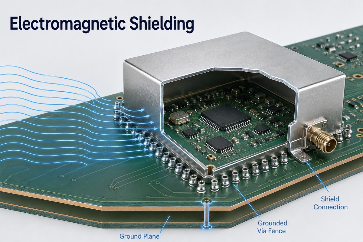
Electromagnetic shielding is a barrier that attenuates electric, magnetic, or electromagnetic fields between a source and a protected region. In electronics, it helps limit radiated emissions from noisy circuits and improves immunity when sensitive circuits operate near motors, switch-mode power supplies, radios, cables, or fast digital interfaces.
A shield may surround an entire product, cover one PCB area, wrap a cable, close an enclosure seam, or form a conductive layer in a flexible circuit. The correct structure depends on the problem frequency and coupling mechanism. A thin conductive shield can perform well against high-frequency electric fields, while low-frequency magnetic fields may require high-permeability material and a different geometry.
How Does Electromagnetic Shielding Work?
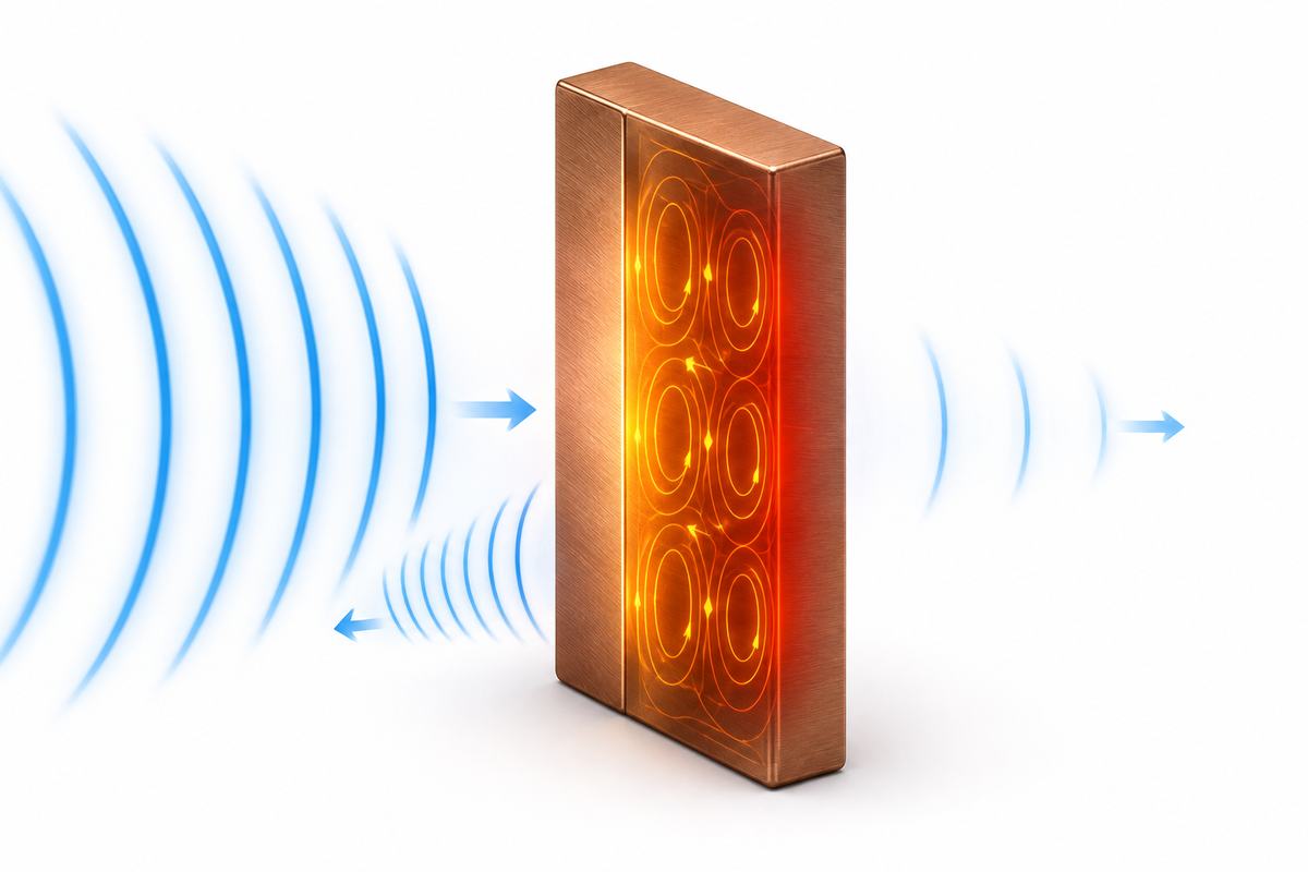
Electromagnetic shielding works mainly through reflection and absorption, with additional internal reflections occurring inside thin or layered materials. Conductive materials support surface currents that oppose an incident field, while magnetic materials can provide a lower-reluctance path for magnetic flux.
- Reflection: impedance changes at the shield surface redirect part of the incident energy.
- Absorption: energy decays as currents flow through a lossy conductive or magnetic material.
- Multiple reflection: energy can reflect between material boundaries, especially in thin, porous, or layered shields.
This is the practical core of electromagnetic shielding theory and applications: performance depends on field type, frequency, material properties, thickness, distance from the source, and electrical continuity. A material data sheet alone cannot predict the finished enclosure or PCB assembly.
Which Electromagnetic Shielding Materials Are Used?
The most useful electromagnetic shielding materials are chosen for conductivity, magnetic permeability, corrosion behavior, mechanical form, solderability, weight, and cost. No material is universally best across all frequencies and product structures.
| Material or Structure | Main Strength | Common Use | Main Limitation |
| Copper | High conductivity and solderability | Foils, tapes, PCB planes, cable shields | Weight, cost, and galvanic compatibility |
| Aluminum | Good conductivity at low weight | Enclosures, foil, covers | Oxide layer and joining method need attention |
| Tin-plated steel | Formability, solderability, and economical construction | Board-level shield cans | Greater weight than aluminum |
| Nickel silver | Corrosion resistance and practical shield-can forming | Removable and soldered PCB shields | Higher material cost than basic steel |
| High-permeability alloy | Redirects low-frequency magnetic flux | Transformers, sensors, magnetic-field control | Forming and mechanical stress can affect performance |
| Conductive elastomer or fabric | Maintains electrical contact across joints | Gaskets, doors, seams, serviceable covers | Compression, aging, plating compatibility, and contact resistance |
Material selection must include the surrounding metals and environment. Dissimilar metals, moisture, salt, coatings, and repeated opening can increase contact resistance or corrosion risk. For a shield can, the solderable finish and mechanical flatness may matter as much as the base metal.
How Is Electromagnetic Shielding Effectiveness Measured?
Electromagnetic shielding effectiveness is the reduction in field level produced by a shield, normally expressed in decibels at a stated frequency and test condition. For electric-field amplitude, 20 dB represents a 10:1 reduction, 40 dB a 100:1 reduction, and 60 dB a 1000:1 reduction.
The number is meaningful only when the test method, frequency range, sample geometry, field type, and fixture are known. ASTM D4935 is commonly used for planar material samples, while IEEE 299 addresses shielding enclosures. A tape sample measured in a laboratory fixture should not be assumed to deliver the same result after it is applied across a painted seam, around a connector, or inside a vented product.
- Define the required frequency range and field type.
- Match the test method to the material, enclosure, cable, or finished product.
- Record apertures, seams, grounding, gasket compression, and cable configuration.
- Compare data only when the test conditions are reasonably equivalent.
What Is the Difference Between EMI and EMC Shielding?
EMI describes unwanted electromagnetic interference, while EMC describes a product’s ability to operate correctly in its electromagnetic environment without causing unacceptable interference. Shielding is one technique used to improve EMC; it does not replace source suppression, filtering, grounding, return-path control, or compliance testing.
A product can fail because it emits too much noise or because it is too susceptible to an external field. The same enclosure may help both problems, but the coupling paths can differ. Designers should therefore identify the source, path, victim, frequency, operating mode, and cable state before choosing a shield.
Which Shielding Method Fits the Interference Path?
The shielding method should match the dominant path rather than the visible symptom. Radiated noise, conducted noise, cable common-mode current, enclosure leakage, and local component coupling require different controls.
| Interference Path | Useful Controls | Validation Focus |
| PCB trace or switching loop radiation | Smaller loop area, continuous return plane, source filtering, local shield | Near-field scan and radiated emissions |
| Cable common-mode current | Connector filtering, 360-degree shield termination, common-mode control | Cable-current probe and system configuration |
| Enclosure seam or aperture leakage | Shorter openings, conductive gasket, overlapping joint, reliable bonding | Seam scan and enclosure test |
| Local circuit-to-circuit coupling | Placement separation, ground fencing, board-level shield can | Victim-node noise and functional immunity |
| Low-frequency magnetic field | Distance, loop orientation, lower source current, high-permeability shield | Magnetic probe and operating-current condition |
How Should Electromagnetic Shielding Be Applied to PCB Design?
PCB shielding should begin with current-path control, because a metal can cannot correct every layout problem. Keep high di/dt loops compact, place decoupling close to device pins, use continuous reference planes, and prevent fast return currents from crossing plane splits or connector cutouts.
- Identify switching nodes, clocks, RF sections, cables, and sensitive analog circuits.
- Minimize source-loop area and keep return paths directly adjacent to critical signals.
- Partition noisy and sensitive functions by placement and routing, not by arbitrary ground splitting.
- Place stitching vias where return current changes reference or where a shield perimeter needs a low-inductance ground connection.
- Define connector-shell, chassis-ground, and signal-ground relationships in the schematic and mechanical design.
- Reserve shield-can pads, keep-outs, rework access, and component-height clearance before layout release.
Our guides to PCB ground-plane layout and high-speed PCB design cover the return-path and stackup details that should be resolved before shielding hardware is added.
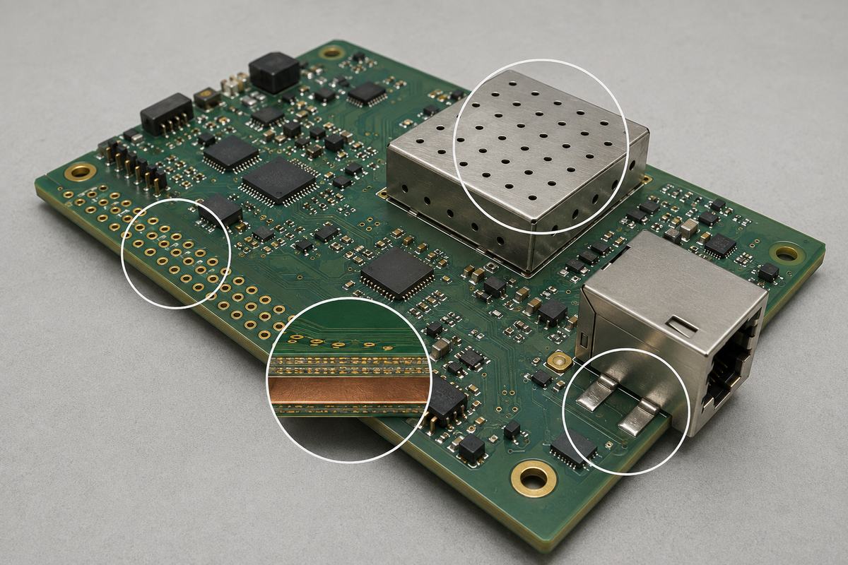
When Should You Use PCB Shielding Cans?
A PCB shielding can is useful when a localized RF, clock, converter, or sensitive receiver section needs additional isolation after the layout and grounding have been optimized. One-piece cans suit permanent coverage, while two-piece frame-and-lid structures improve inspection, tuning, and rework access.
The can needs a continuous, low-inductance connection to the intended ground reference. Its perimeter pads, via stitching, wall height, vent pattern, component clearance, and reflow process must be designed together. Our board-level shielding guide explains can materials, grounding, apertures, and assembly choices in detail.
When Is Electromagnetic Shielding Tape Useful?
Electromagnetic shielding tape is useful for prototypes, seams, cable wrapping, local conductive patches, and surfaces that cannot be soldered directly. Copper, tin-plated copper, and aluminum foil tapes are available with conductive adhesive, but the backing material alone does not guarantee a low-impedance joint.
Check whether the adhesive conducts through its thickness, whether the overlap remains conductive, and whether the tape bonds to bare metal, plating, paint, or plastic. Surface cleanliness, bending radius, oxidation, galvanic compatibility, temperature, humidity, and long-term peeling can all change the result. Tape is excellent for controlled applications and debugging, but it should not hide an unresolved production-design problem.
Why Do Seams, Apertures, and Cables Cause Leakage?
Seams, apertures, and cables cause leakage because they interrupt the shield current or provide a path for common-mode energy to cross the barrier. The longest dimension of a slot is often more important than its total area, so one long opening can leak more than several small holes.
- Use many small ventilation holes instead of a long slot when airflow permits.
- Maintain conductive contact around serviceable seams with suitable gaskets or spring fingers.
- Bond connector shells to the intended chassis or shield reference with a short, wide connection.
- Filter or shield conductors at the point where they cross the enclosure boundary.
- Control coatings, paint, anodizing, and contamination at intentional contact surfaces.
The system drawing should state which contacts are intentional. The distinction between board ground, shield ground, chassis, and protective earth is explained in our GND and earth guide.
How Do You Test and Validate an EMI Shield?
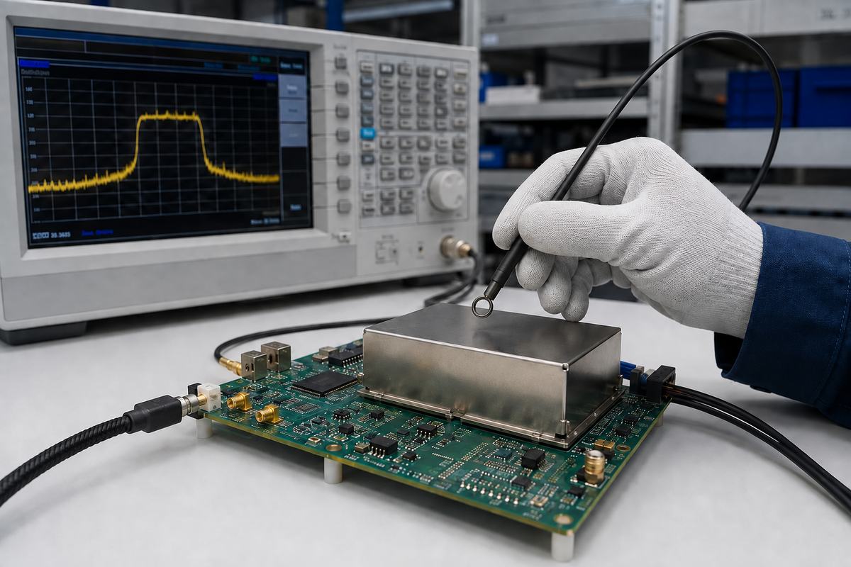
An EMI shield is validated by testing the assembled product in representative operating modes, cable configurations, and mechanical conditions. Material certificates and continuity measurements are useful inputs, but they cannot replace a system-level emissions or immunity evaluation.
- Establish a baseline: measure the unshielded design or an earlier build under repeatable conditions.
- Locate the source: use near-field electric and magnetic probes to identify hot loops, seams, and cables.
- Change one variable: add a can, gasket, tape, filter, or grounding change without mixing several unknowns.
- Run pre-compliance checks: compare emissions across the relevant frequency range and product modes.
- Verify the final assembly: test with production fasteners, covers, coatings, cables, and software states.
- Complete required compliance testing: use the standards and limits applicable to the product and destination market.
For U.S. unintentional radiators, FCC guidance points to defined Part 15 measurement procedures; other markets and product categories may require CISPR, IEC, automotive, aerospace, medical, or customer-specific methods. The applicable standard must be identified for the finished product rather than inferred from the PCB alone.
Frequently Asked Questions About Electromagnetic Shielding
What is the most effective material for electromagnetic shielding?
There is no single most effective material for every case. Copper and aluminum work well for many high-frequency electric-field and plane-wave problems, while high-permeability alloys are more suitable for some low-frequency magnetic fields. The enclosure geometry, seams, apertures, grounding, frequency, corrosion environment, and test method usually determine the finished result.
Does thicker metal always improve shielding?
No. Thickness can improve absorption when it is small relative to the required attenuation, but at high frequency a thin conductive layer may already exceed several skin depths. Leakage through seams, vents, connectors, and poor bonds can then dominate. Increasing wall thickness will not repair an electrically open joint or an unfiltered cable penetration.
Does an EMI shield always need to be grounded?
Not every shield requires a DC earth connection, but most practical PCB and enclosure shields need a controlled low-impedance relationship to the intended reference. The correct connection depends on frequency, safety architecture, cable termination, ESD path, and enclosure design. A long wire that looks grounded at DC may behave inductively at RF.
Can aluminum foil block electromagnetic interference?
Aluminum foil can attenuate some high-frequency electric fields when it forms a continuous enclosure with controlled seams and connections. A loose sheet or incomplete wrap is not equivalent to a qualified shield. Openings, oxide at contact points, cable entry paths, mechanical durability, and the field frequency determine practical effectiveness.
Can shielding fix a poor PCB layout?
Shielding can reduce residual radiated coupling, but it cannot reliably correct every return-path, common-mode, decoupling, or cable-current problem. Source suppression and layout correction usually provide a more stable foundation. Use a shield after the dominant source and coupling path are understood, not as a substitute for that analysis.
How should shielding effectiveness data be compared?
Compare data only when frequency, test method, fixture, sample size, field condition, and assembly details are stated. A planar material test, gasket test, shielded-room test, and finished-device radiated-emissions test answer different questions. Ask for the original test standard and configuration instead of comparing only the highest dB number.
How Can EBest Circuit Support EMI-Sensitive PCB Projects?
At EBest Circuit, we support PCB fabrication and assembly projects that require controlled stackups, continuous reference planes, shield-can landing patterns, via structures, solder-mask openings, and inspection of assembled shielding hardware. The released files should define the intended ground nets and mechanical contacts clearly so production does not have to guess.
Send us your Gerber or ODB++ data, stackup, BOM, shield-can drawing, enclosure interface, quantity, and test requirements. We can review the manufacturability of the PCB and assembly details before production and provide technical support and a quotation at sales@bestpcbs.com.