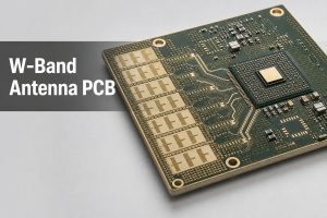
An RF amplifier, or radio frequency amplifier, increases the amplitude or power of an RF signal within a specified frequency range. Depending on where it sits in the signal chain, it may amplify a weak received signal, drive another RF stage, or provide enough output power for transmission. Gain, noise figure, bandwidth, linearity, output power, efficiency, and impedance matching are the main parameters that define its performance.
RF amplifiers are used in wireless communication, radar, satellite systems, test equipment, IoT hardware, MRI equipment, and many other RF products. Their real performance depends not only on the amplifier IC or transistor, but also on the matching network, bias circuit, PCB layout, grounding, stackup, and thermal design.
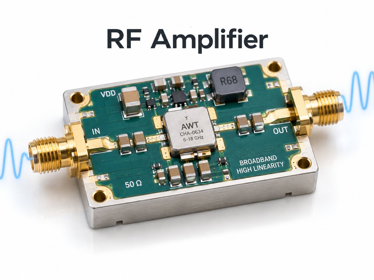
What Is an RF Amplifier?
An RF amplifier is a circuit that strengthens a radio-frequency signal without changing its intended information content.
The term covers several amplifier functions. A receiver may use a low-noise amplifier to raise a weak antenna signal. A transmitter may use a driver amplifier followed by an RF power amplifier to increase signal power before the antenna.
Typical RF amplifier roles include:
- Low-noise amplification in receiver front ends
- Signal gain between RF stages
- High-linearity amplification for modulated signals
- Wideband amplification across multiple frequencies
- Power amplification before transmission
- Adjustable gain for automatic gain control
An RF amplifier is therefore broader than an RF power amplifier. A power amplifier is only one category within the RF amplifier family.
At radio and microwave frequencies, parasitic capacitance, inductance, trace impedance, return-current paths, and electromagnetic coupling become part of the circuit behavior. That is why RF amplifiers require more careful physical implementation than ordinary low-frequency amplifiers.
How Does an RF Amplifier Work?
An RF amplifier uses energy from a DC power supply to increase the level of an incoming RF signal.
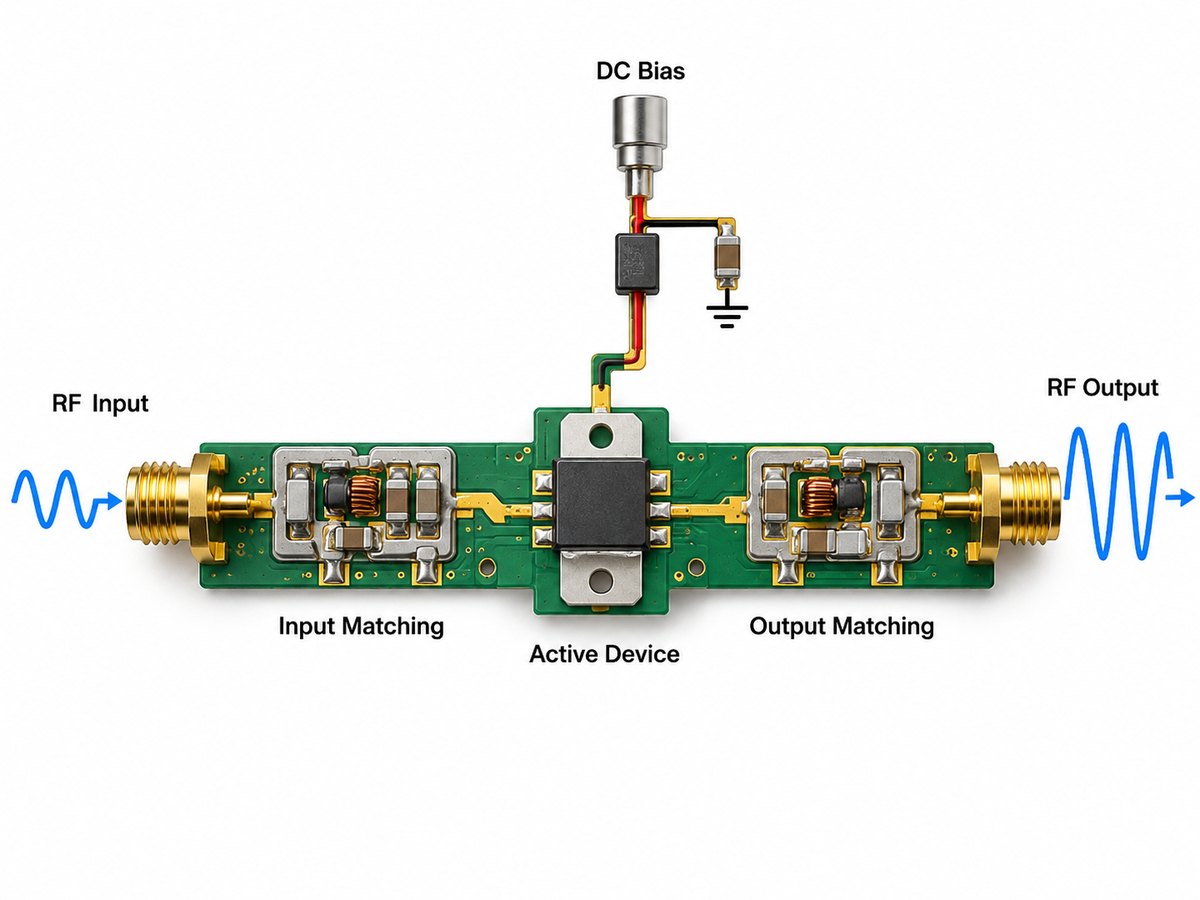
A simplified RF signal path is:
RF input → input matching → active device → output matching → RF output
The active device may be a transistor, MMIC, or integrated RF amplifier IC. The surrounding network allows that device to operate at the required frequency and bias point.
A typical circuit includes:
- Input matching network to interface the source with the amplifier
- Active device to provide gain
- Bias circuit to set the correct DC operating condition
- Output matching network to transfer power to the next stage
- Decoupling components to keep RF energy out of the power rail
- DC blocking capacitors where RF and DC paths must be separated
At low input levels, the amplifier normally operates in its linear region. As input power rises, the output eventually stops increasing proportionally. This is the beginning of gain compression, which is why RF designers check parameters such as P1dB when defining the usable signal range.
What Are the Main Types and Classes of RF Amplifiers?
RF amplifiers are usually classified first by what they do in the RF signal chain.
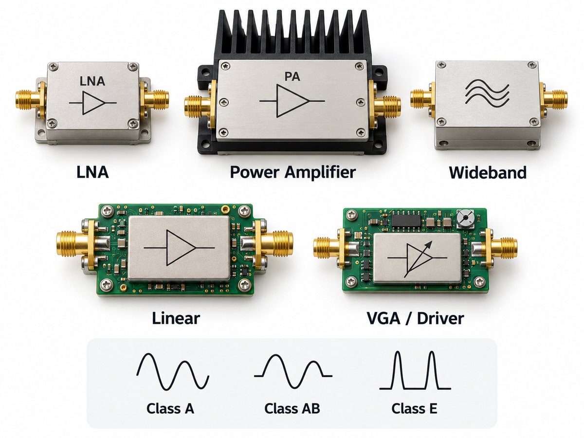
Low-noise amplifier
A low-noise RF amplifier, or LNA, is used near the receiver input. Its main job is to amplify weak signals while adding as little noise as possible.
RF power amplifier
An RF power amplifier increases signal power before transmission. Output power, efficiency, linearity, and thermal performance are usually the main concerns.
Wideband RF amplifier
A wideband amplifier provides useful gain across a broad frequency range. It is common in test equipment, broadband communication, radar, and multi-band RF systems.
RF linear amplifier
A linear RF amplifier is designed to preserve the amplitude and phase characteristics of the input waveform. This matters for modulation schemes that are sensitive to distortion.
Variable gain amplifier
A VGA allows gain to be changed electronically. It is often used in automatic gain control and systems with a wide input signal range.
Gain block and driver amplifier
A gain block provides convenient fixed gain. A driver amplifier raises the signal level before another stage, often before the final PA.
RF power amplifiers may also be described as Class A, AB, B, C, D, or E. These classes describe how the active device operates.
In simple terms:
- Class A favors linearity
- Class AB balances linearity and efficiency
- Class B and C increase efficiency but reduce linear operation
- Class D and E use switching behavior for higher efficiency in suitable RF designs
Function and operating class are different classifications, so a power amplifier can still be described separately as Class AB, Class E, or another class.
What Does an RF Amplifier Circuit and Schematic Include?
An RF amplifier circuit normally combines an active device with matching, bias, decoupling, and filtering networks.
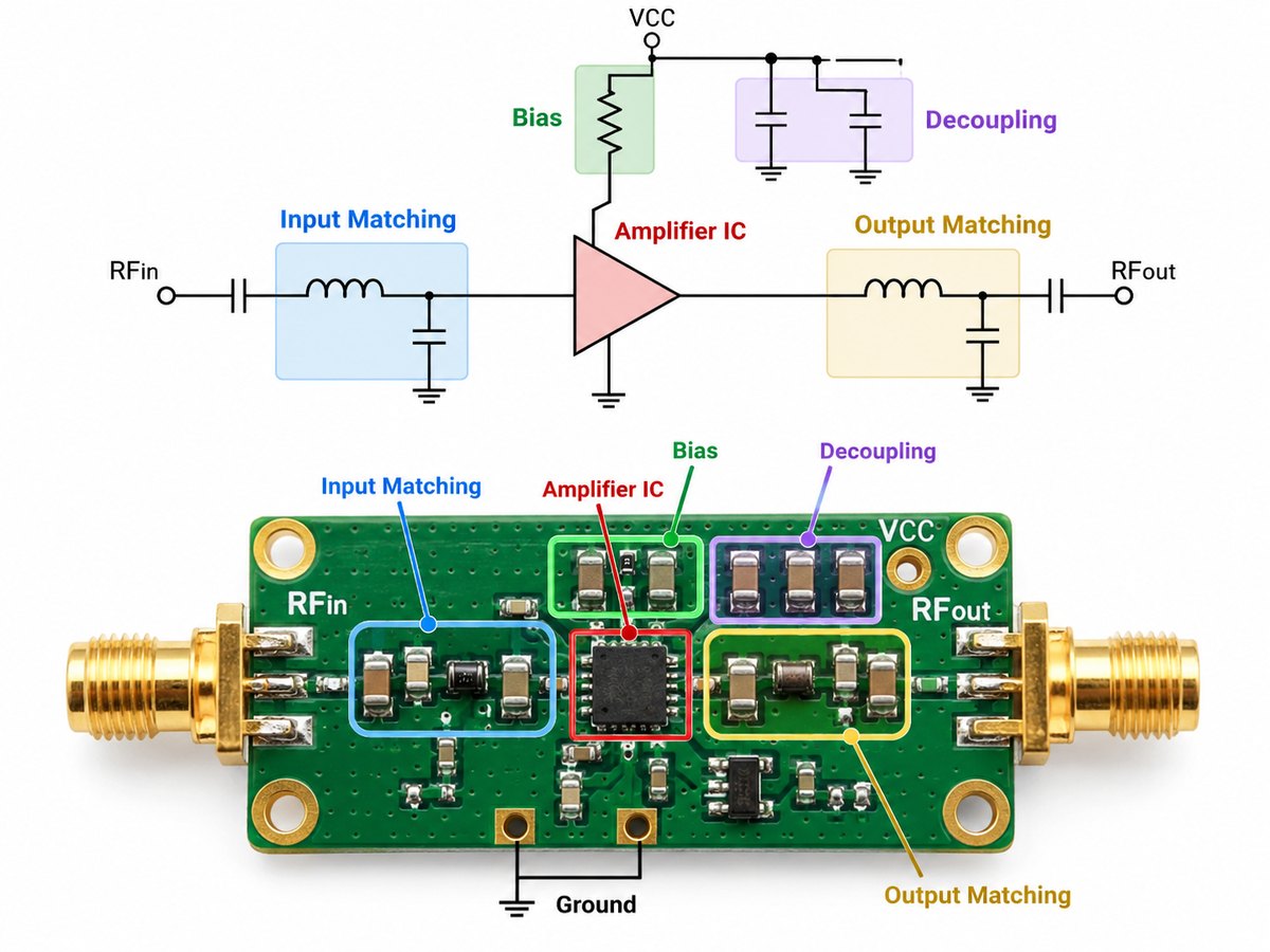
The main parts shown in an RF amplifier schematic are typically:
- Transistor, MMIC, or RF amplifier IC
- Input matching components
- Output matching components
- Bias resistors, inductors, or RF chokes
- DC blocking capacitors
- Power-supply bypass capacitors
- Ground connections
- Optional filtering or stability components
The schematic shows the electrical connections, but the physical PCB implementation strongly affects the final RF behavior.
For example, a capacitor connected directly to ground on the schematic still has pad, trace, and via inductance on the real board. At microwave frequencies, even a short connection can change the response of the matching or decoupling network.
RF amplifier circuits may be implemented in three common forms:
- Discrete circuit: transistor plus external bias and matching components
- RF amplifier IC or MMIC: more RF functions integrated into one device
- RF amplifier module: amplifier plus additional matching, shielding, connectors, filtering, or thermal structure
The best form depends on frequency, power, board area, development effort, and performance requirements.
Which RF Amplifier Specifications Matter Most?
The most important RF amplifier specifications are frequency range, gain, noise figure, linearity, output power, matching, and efficiency.
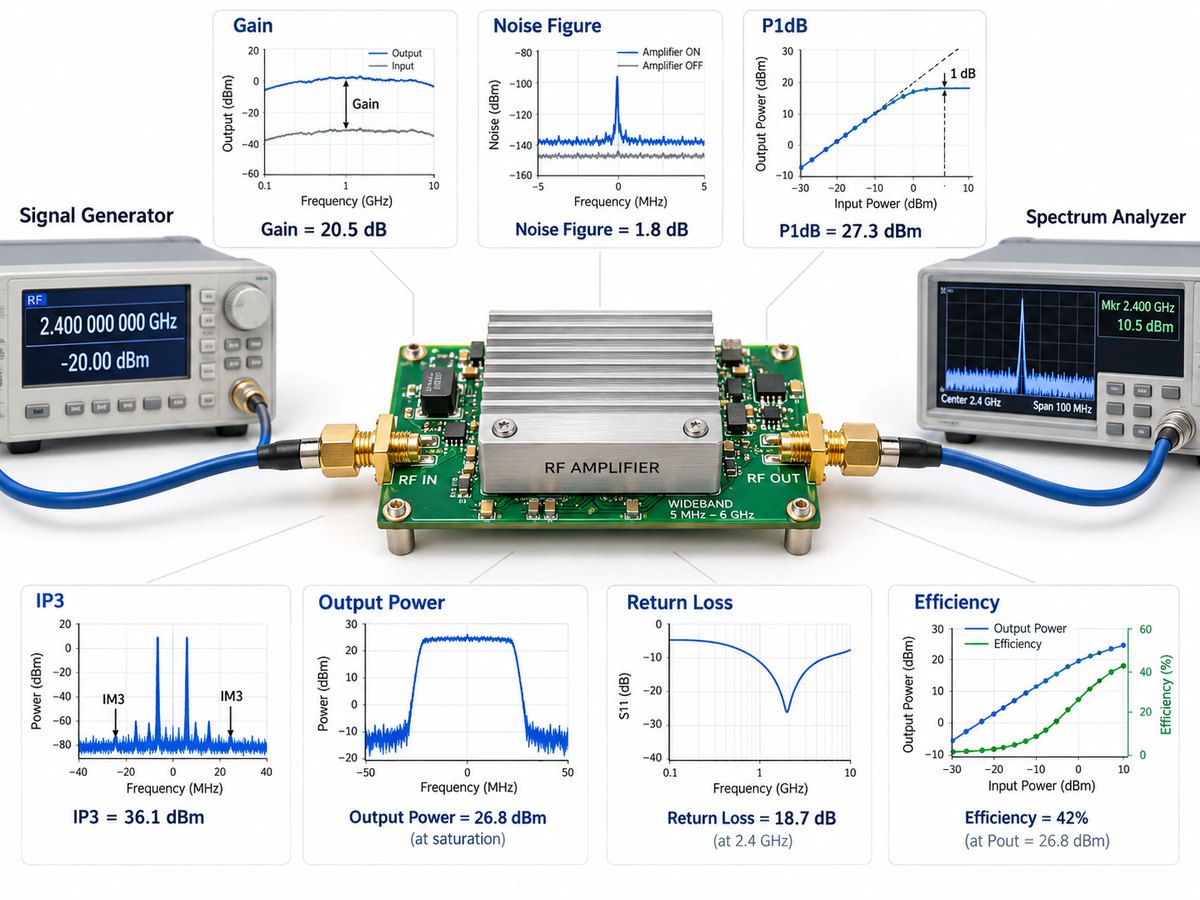
| Specification | What It Indicates | Typical Importance |
| Frequency range | Supported RF band | All RF amplifiers |
| Gain | Signal amplification | All signal chains |
| Gain flatness | Gain variation across bandwidth | Wideband systems |
| Noise figure | Noise added by the amplifier | Receiver LNAs |
| P1dB | Beginning of meaningful gain compression | Large-signal operation |
| IP3 | Intermodulation linearity | Multi-signal environments |
| Output power | Available RF power | Driver and power amplifiers |
| Return loss / VSWR | Input and output matching | RF interfaces |
| Efficiency | DC-to-RF power conversion | Power amplifiers |
| Supply voltage/current | Electrical power requirement | Power and thermal design |
No single specification tells the whole story.
A high-gain amplifier may still be unsuitable if its output compresses too early. A low-noise device may not provide enough linearity in the presence of strong nearby signals. A power amplifier may meet its output-power target but create excessive heat if efficiency is poor.
For wideband designs, these specifications should be checked across the complete operating frequency range rather than only at the center frequency.
How Do Gain, Noise Figure, and Linearity Affect RF Amplifier Performance?
Gain, noise figure, and linearity determine how strongly an RF amplifier boosts the signal, how much noise it adds, and how well it handles larger or multiple signals.
Gain determines how much the signal level rises through the amplifier. Too little gain may leave the next stage with insufficient signal. Too much gain can reduce available headroom.
Noise figure measures how much the amplifier degrades the signal-to-noise ratio. It matters most in the early stages of a receiver, where added noise can directly affect sensitivity.
Linearity describes how well the amplifier avoids distortion as signal level rises. P1dB and IP3 are commonly used to judge this behavior.
These parameters often interact.
For example, increasing front-end gain can reduce the relative noise contribution of later receiver stages. However, the same higher gain may cause the receiver to reach compression sooner when a strong signal enters the system.
The priority depends on amplifier position:
- LNA: noise figure, gain, linearity
- Driver amplifier: gain, IP3, P1dB
- Power amplifier: output power, efficiency, linearity, thermal performance
The correct target is therefore not simply maximum gain or minimum noise, but enough margin for the full signal environment.
How Do You Choose the Right RF Amplifier for an Application?
Choose an RF amplifier by matching its operating limits to the actual frequency, signal level, bandwidth, and system role.
Start with these requirements:
- Operating frequency or frequency range
- Required gain
- Minimum and maximum input level
- Required output power
- Bandwidth
- Noise figure limit
- P1dB and IP3 targets
- Modulation and linearity requirements
- Supply voltage and current
- Efficiency target
- Operating temperature
- Package or module size
- Input and output impedance
For a receiver front end, noise figure and linearity are usually more important than maximum output power.
For a transmitter, output power, efficiency, linearity, compression, and thermal performance move higher on the list.
For a wideband RF amplifier, check that gain flatness, return loss, noise figure, and output performance stay acceptable across the full band.
It is also useful to check whether the manufacturer provides a validated evaluation-board layout. RF amplifier performance can change noticeably when the matching network or PCB geometry differs from the reference design.
What Causes RF Amplifier Instability and Oscillation?
RF amplifier instability is usually caused by unintended feedback, poor grounding, incorrect matching, or parasitic coupling.
Common causes include:
- Coupling between RF input and output
- Long or poorly controlled RF traces
- Weak ground connections
- Insufficient power-supply decoupling
- Bias network problems
- Incorrect matching components
- Parasitic capacitance and inductance
- Coupling through power or ground networks
- Layout changes from the reference design
- Poor isolation from digital or switching circuits
Oscillation may occur inside or outside the intended RF band. It can raise current consumption, increase noise, distort gain, or produce unexpected spectral components.
Several layout practices help reduce the risk:
- Keep input and output networks physically separated
- Place decoupling components close to the device pins
- Use short ground paths
- Add ground vias where needed
- Keep switching power circuits away from sensitive RF sections
- Preserve the intended matching-network geometry
For discrete RF amplifier design, stability should also be checked in simulation over a frequency range wider than the required operating band.
What PCB Design Factors Affect RF Amplifier Performance?
RF amplifier PCB performance depends heavily on controlled impedance, grounding, component placement, isolation, dielectric properties, and thermal design.
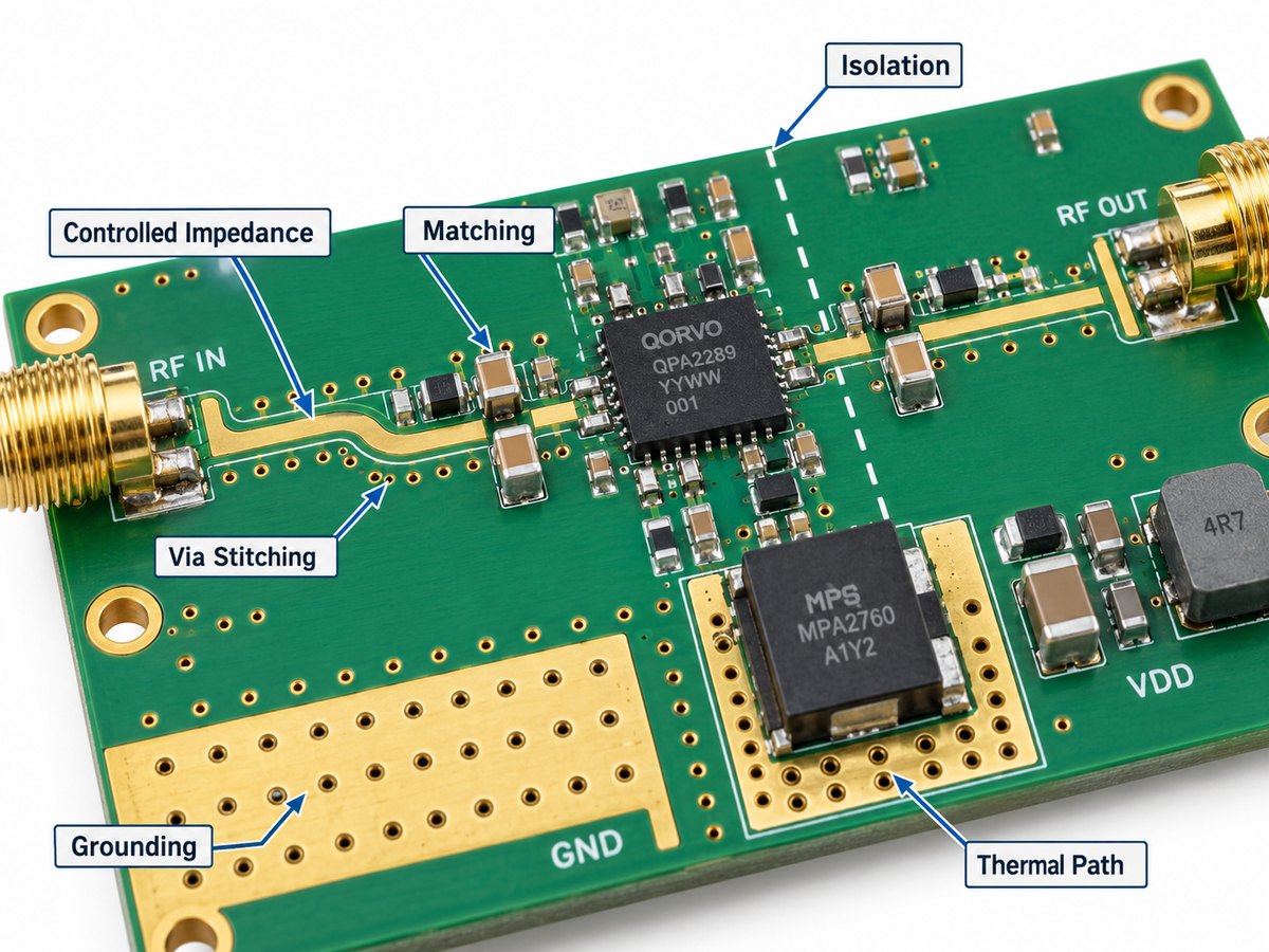
Controlled impedance
RF traces are commonly designed as microstrip, stripline, or grounded coplanar waveguide. Their impedance depends on trace width, copper thickness, dielectric thickness, Dk, and nearby reference conductors.
RF trace routing
Critical RF paths should remain compact and free from unnecessary bends or discontinuities. The production routing should stay close to the geometry used during simulation or reference-board validation.
Grounding
A continuous ground reference helps maintain a predictable RF return path. Ground-plane gaps or long ground connections add unwanted inductance.
Matching-network placement
Matching capacitors and inductors should be positioned close to the RF device and in the intended order. At higher frequencies, moving these components can alter the matching response.
Via stitching
Ground stitching vias can help maintain plane continuity and reduce field spreading around RF structures.
Isolation
Keep RF inputs away from high-power RF outputs, clocks, DC/DC converters, and fast digital signals to reduce unwanted coupling.
PCB material
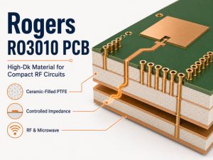
Higher-frequency or lower-loss designs may require RF laminates with more stable Dk and lower dissipation loss than standard FR-4. Material selection should match the loss budget, frequency, stackup, and cost target.
Thermal path
Power amplifiers may require:
- Exposed thermal pads
- Thermal vias
- Heavy local copper
- Heat spreaders
- Metal chassis contact
- Dedicated heatsinks
The fabricated PCB stackup should match the stackup used for impedance calculation and RF simulation. Changes to dielectric thickness, copper weight, or laminate grade can alter the final RF transmission-line geometry.
If your project is already moving from amplifier selection to board layout, our RF amplifier PCB guide explains the PCB-level checks that should be reviewed before fabrication and assembly.
Where Are RF Amplifiers Used?
RF amplifiers are used in receivers, transmitters, measurement equipment, medical systems, radar, wireless hardware, and microwave electronics.
Common applications include:
- Cellular base stations
- Wi-Fi and 2.4 GHz wireless devices
- Bluetooth and IoT products
- Satellite communication
- Radar
- GNSS receivers
- Software-defined radio
- RF test instruments
- Microwave communication links
- Radio transmitters
- MRI systems
- Industrial RF equipment
- RF distribution systems
- Aerospace and defense electronics
The amplifier type depends on the position in the system.
A receiver may use an LNA to raise a weak antenna signal. A transmitter may use a driver amplifier followed by a power amplifier. Test equipment may use wideband or variable gain amplifiers to support multiple frequency ranges and signal levels.
A 2.4 GHz RF amplifier, for example, can be used in either the receive or transmit chain. The required gain, noise figure, power, and linearity will differ depending on that role.
FAQ About RF Amplifiers
1. What does RF amplifier stand for?
RF amplifier stands for radio frequency amplifier. It amplifies RF signals used in wireless, radio, radar, satellite, and other high-frequency electronic systems.
2. What is the difference between an RF amplifier and an RF power amplifier?
An RF amplifier is the general category. An RF power amplifier is a specific type designed to deliver higher RF output power, usually near the transmitter output.
3. What is the difference between an LNA and a power amplifier?
An LNA amplifies weak received signals while adding very little noise. A power amplifier increases RF power for transmission or for driving another high-power stage.
4. What does gain mean in an RF amplifier?
Gain is the increase in signal level from the amplifier input to its output. RF power gain is usually expressed in decibels, or dB.
5. Why are RF amplifiers usually designed for 50 ohms?
Many RF cables, connectors, instruments, antennas, and components use 50 Ω interfaces, so 50 Ω has become a common system standard. Matching networks may still be required because the amplifier device itself may not have a native 50 Ω impedance.
6. Can an RF amplifier work at 2.4 GHz?
Yes. Many RF amplifiers are designed for the 2.4 GHz band. The device must support the required frequency while meeting the target gain, noise figure, output power, linearity, and matching requirements.
Ready to Move Your RF Amplifier Design Into PCB Production?
RF amplifier performance can change when the production PCB does not reproduce the intended stackup, impedance, grounding, matching geometry, component placement, or thermal path.
EBest Circuit supports RF and microwave PCB and PCBA projects using controlled impedance, Rogers materials, Rogers/FR-4 hybrid stackups, low-loss multilayer construction, HDI, fine-pitch assembly, impedance verification, and engineering DFM review. Send your Gerber files, stackup, BOM, target impedance, operating frequency, assembly requirements, and quantity to sales@bestpcbs.com for review and quotation.