High-speed PCB materials should be selected by insertion-loss budget, Df, Dk stability, copper roughness, dielectric thickness, glass weave, impedance target and manufacturing availability. FR-4 may still work for shorter channels, while low-loss laminates are better for longer or tighter-margin SerDes links.
That does not mean every high-speed PCB needs an ultra-low-loss laminate. Standard or enhanced FR-4 can still work well for shorter channels with enough margin. Low-loss materials become more useful when longer SerDes links, dense routing, multiple vias, or tighter insertion-loss targets leave less room for error.
What Are High-Speed PCB Materials?
High-speed PCB materials are laminate and dielectric systems chosen for predictable electrical behavior at higher signal frequencies and edge rates.
They may include:
- standard FR-4
- enhanced FR-4
- mid-loss epoxy laminates
- low-loss and very-low-loss laminates
- hydrocarbon ceramic materials
- PTFE-based materials
A high-speed PCB is not defined only by clock frequency. Fast rise and fall times can make a trace behave like a transmission line even when the nominal clock looks relatively low.
Once trace length becomes electrically significant, the design must account for:
- controlled impedance
- reflections
- dielectric loss
- conductor loss
- return-path continuity
- timing skew
This is why specifying only “FR-4” or “low-loss material” is rarely enough. The laminate grade, dielectric thickness, copper type, and stackup should be reviewed together.
Which PCB Material Properties Matter Most at High Speed?
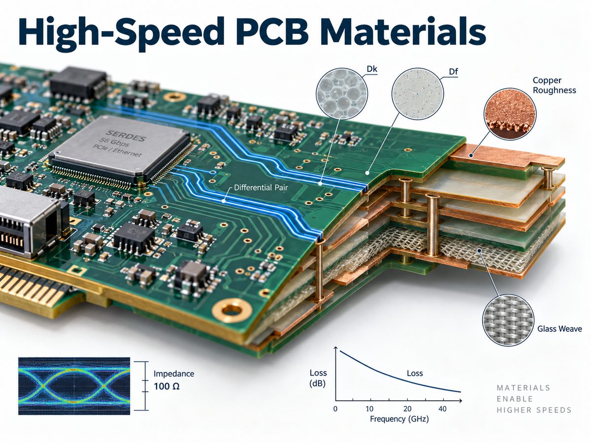
For most high-speed digital boards, the most useful properties to review are Df, Dk stability, copper roughness, and dielectric construction.
| Property | Why It Matters |
| Df | Influences dielectric loss and insertion loss |
| Dk | Affects impedance and propagation delay |
| Dk stability | Helps maintain impedance and timing consistency |
| Copper roughness | Increases conductor loss at high frequency |
| Dielectric thickness | Determines controlled-impedance geometry |
| Glass weave | Can contribute to differential skew |
| Tg / Td | Affects thermal reliability |
| CTE | Influences via and plated-hole reliability |
| Moisture absorption | Can change electrical behavior |
| CAF resistance | Matters for dense spacing and long-term reliability |
Dissipation factor, or Df, is often one of the first parameters engineers compare. Standard FR-4 may fall roughly in the 0.015–0.025 range, while low-loss laminates can be below 0.010 and very-low-loss systems may fall below 0.005.
Dielectric constant, or Dk, affects impedance and signal velocity. A lower Dk can be useful, but consistency is often more important than simply choosing the lowest available value.
A material change may require new:
- trace widths
- differential spacing
- dielectric thicknesses
- copper thickness assumptions
That is why impedance calculations should be tied to the actual production stackup.
What Types of PCB Dielectric Materials Are Used for High-Speed Applications?
PCB dielectric materials for high-speed applications usually fall into four practical groups.
A PCB material for RF applications may also suit some high-speed digital channels, but the final choice must match the channel loss, impedance, thermal, and fabrication requirements.
| Material Family | Typical Use | Relative Loss | Manufacturing Consideration |
| Standard / enhanced FR-4 | General digital, shorter high-speed links | Moderate | Widely available and economical |
| Mid-/low-loss epoxy | Multi-gigabit digital systems | Low | Often processed similarly to FR-4 |
| Hydrocarbon ceramic | High-speed digital, RF, mixed-signal | Low to very low | Requires closer stackup control |
| PTFE-based material | RF, microwave, mmWave, very-low-loss channels | Very low | Requires more specialized fabrication |
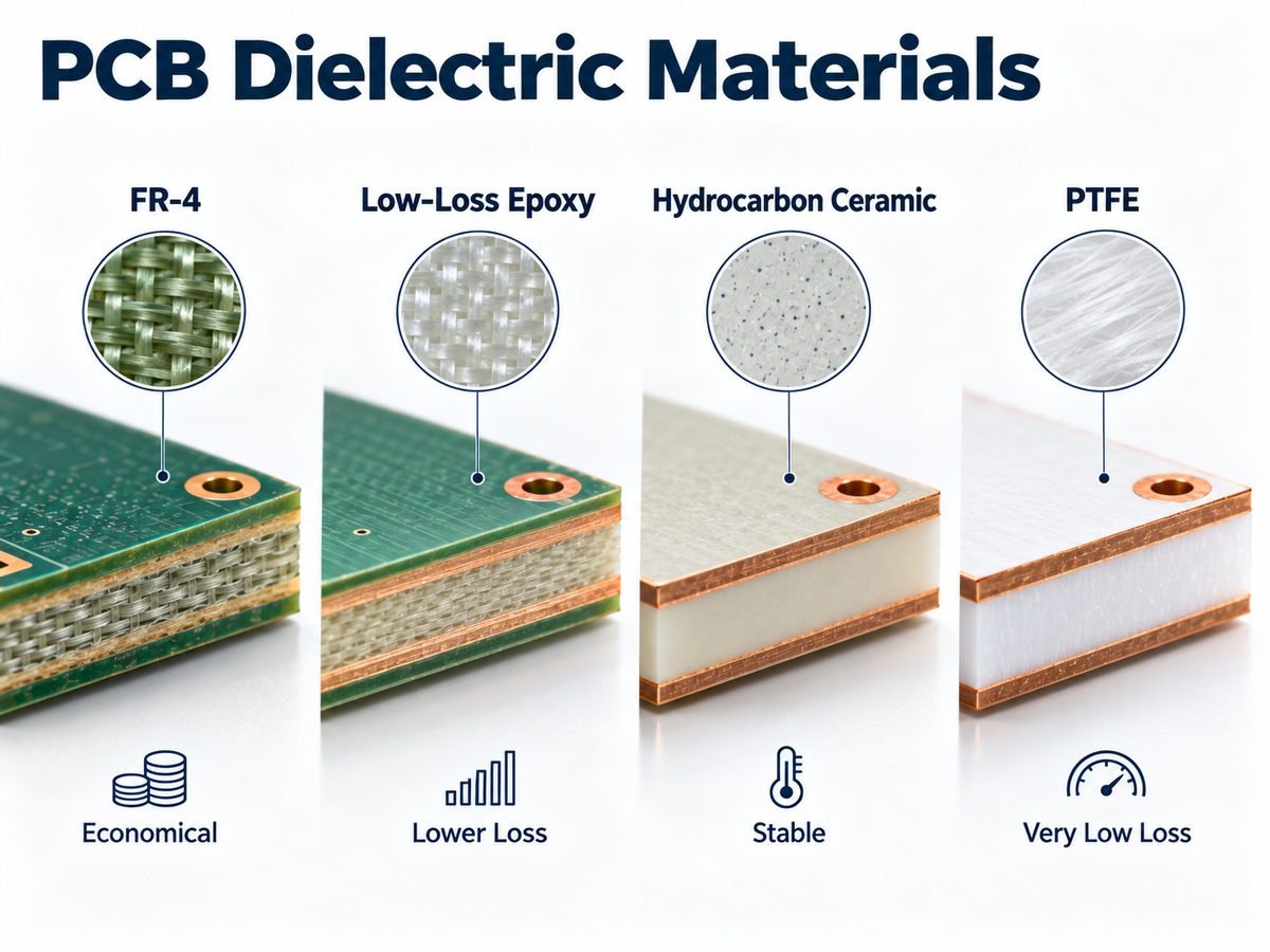
Standard and enhanced FR-4 remain useful because they are economical, widely stocked, and familiar to most PCB manufacturers. Their main limitation in high-speed work is higher loss over long channels.
Low-loss epoxy laminates are a common next step for networking, telecom, data-center, and AI hardware. They reduce dielectric loss without always introducing the fabrication complexity associated with more specialized RF materials.
Hydrocarbon ceramic materials suit designs that need low loss, stable electrical properties, or a mix of high-speed digital and RF functions.
PTFE-based materials offer very low loss, but they usually need tighter process control and are best reserved for applications that genuinely require them.
Material family should be selected first. The exact product grade can then be chosen according to electrical requirements, available constructions, and supplier availability.
How Do FR-4 and Low-Loss PCB Materials Compare?
The biggest difference between FR-4 and low-loss laminates is the amount of channel loss they introduce over distance and frequency.
| Comparison | Standard FR-4 | Low-Loss Laminate |
| Dielectric loss | Higher | Lower |
| Typical Df | Often ~0.015–0.025 | Commonly below ~0.010 |
| Long high-speed channels | More limited | Better suited |
| Material cost | Lower | Higher |
| Availability | Very broad | Grade-dependent |
| Fabrication familiarity | Excellent | Usually good |
| Stackup flexibility | High | Depends on stocked constructions |
| Insertion-loss margin | Lower | Higher |
| Best fit | Shorter, cost-sensitive channels | Longer, loss-sensitive channels |
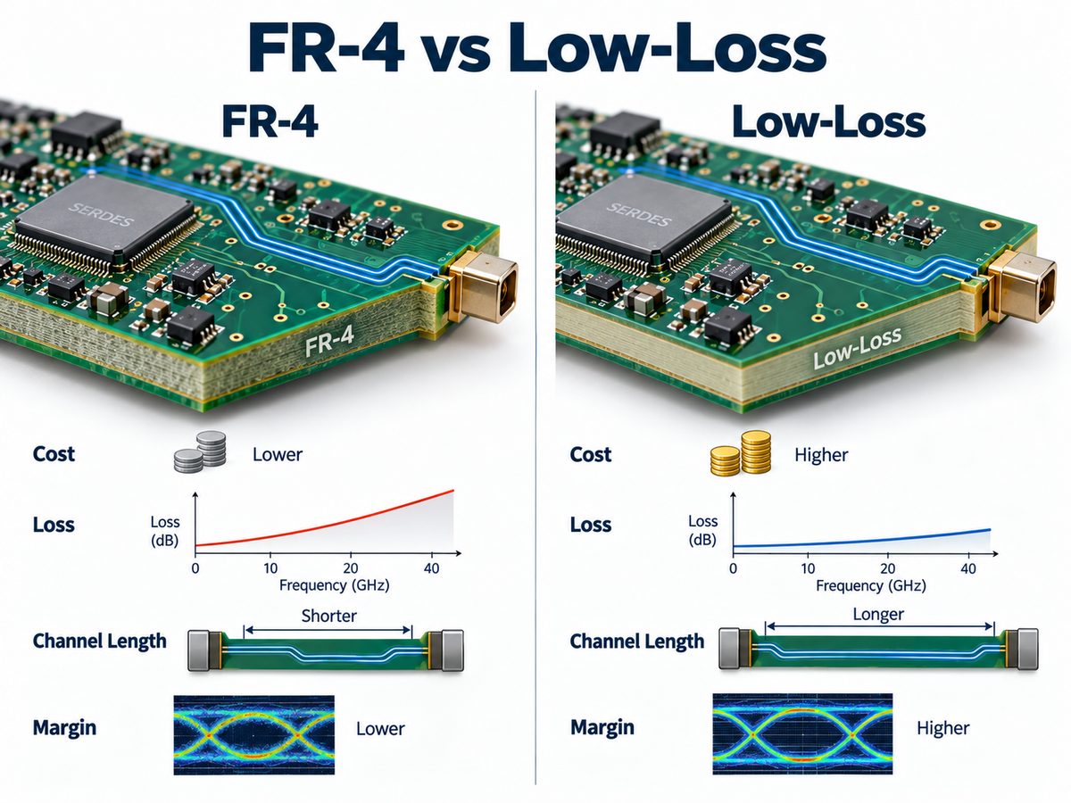
The laminate is only part of the channel. Copper profile, routing length, vias, and connectors can change the result significantly.
For example, a low-Df laminate paired with rough copper may not perform as well as expected. An enhanced FR-4 system with smoother copper and shorter routes may be perfectly adequate.
So material selection should be based on total channel performance rather than one datasheet value.
When Is FR-4 Still Suitable for a High-Speed PCB?
FR-4 is still suitable when the complete interconnect remains inside the required loss, timing, and impedance limits.
There is no universal point where FR-4 suddenly becomes unusable.
FR-4 is often a reasonable choice when:
- high-speed traces are relatively short
- insertion-loss margin is comfortable
- the channel contains few connectors or via transitions
- impedance can be achieved with practical trace geometry
- the selected FR-4 grade has acceptable Df and Dk stability
- project cost is sensitive to material upgrades
Moving to a lower-loss laminate becomes more attractive when the design has:
- longer routed channels
- higher SerDes data rates
- more connectors
- more via transitions
- tight eye-diagram margin
- backplane routing
- higher routing density
- stricter insertion-loss targets
A more expensive laminate will not correct a poor interconnect structure. If the main problem is a long via stub, an interrupted return path, or a badly designed connector transition, the geometry still needs to be fixed.
How Do Dk, Df, Copper Roughness and Glass Weave Affect Signal Integrity?
These factors influence different parts of the channel.
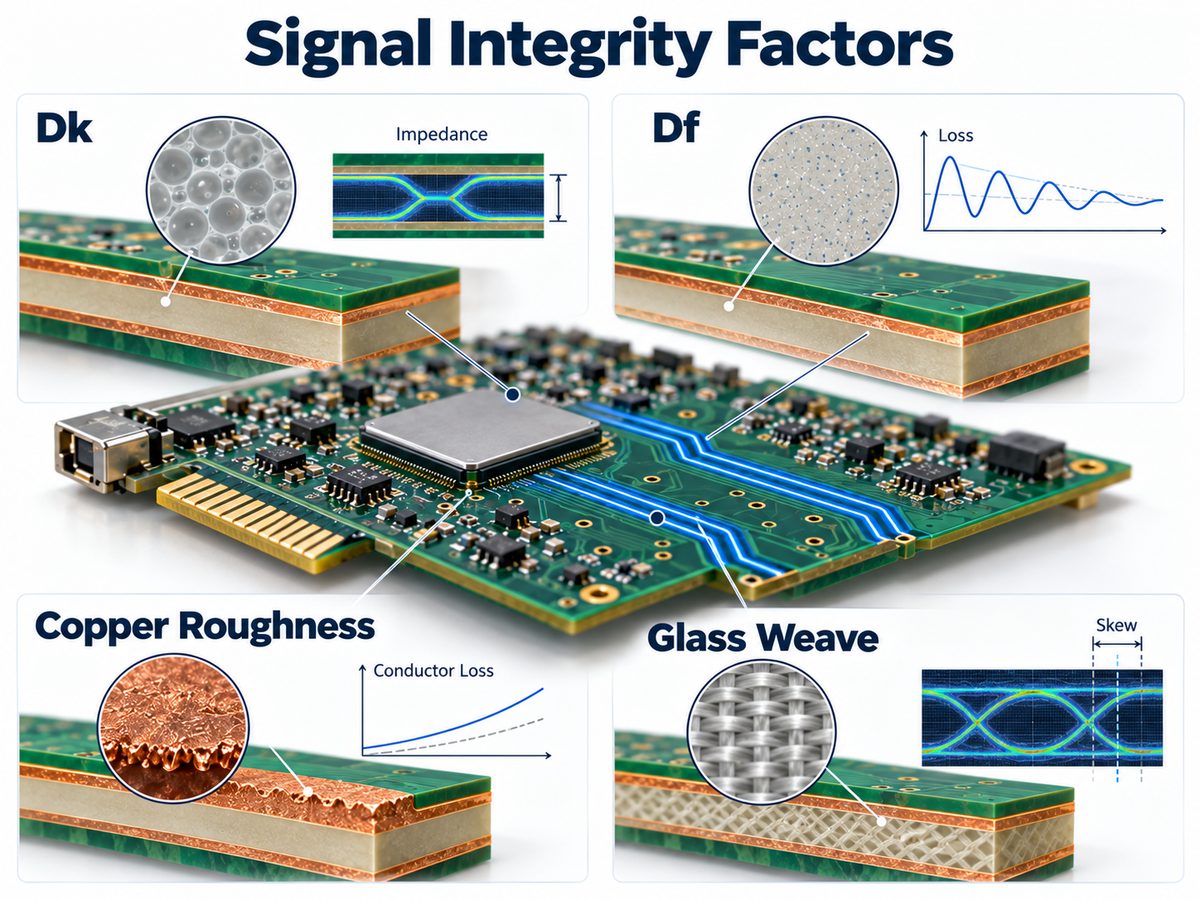
Df affects dielectric loss. Part of the signal energy is dissipated in the dielectric as the signal propagates. Higher Df generally means more attenuation, especially over longer traces and at higher frequencies.
Dk affects impedance and signal velocity. Changes in Dk alter characteristic impedance, propagation delay, and the trace dimensions needed to meet a target such as 50 Ω or 100 Ω differential.
Copper roughness affects conductor loss. At high frequency, current flows close to the conductor surface because of skin effect. Rougher copper increases the effective path length and therefore resistance.
For longer channels, designers often review whether the stackup uses:
- standard copper
- reverse-treated copper
- low-profile copper
- very-low-profile copper
Glass weave can contribute to skew. Glass bundles and resin-rich areas do not have identical dielectric properties. If the two traces in a differential pair see different local material environments, propagation delay can differ.
Common mitigation methods include:
- choosing suitable glass styles
- routing pairs at an angle to the weave
- using resin-rich constructions where appropriate
- avoiding unnecessarily long parallel runs aligned with the weave
For demanding links, these details can matter as much as the headline Dk and Df numbers.
How Do You Choose the Right High-Speed PCB Material?
Start with the interface and channel requirement rather than choosing a laminate brand first.
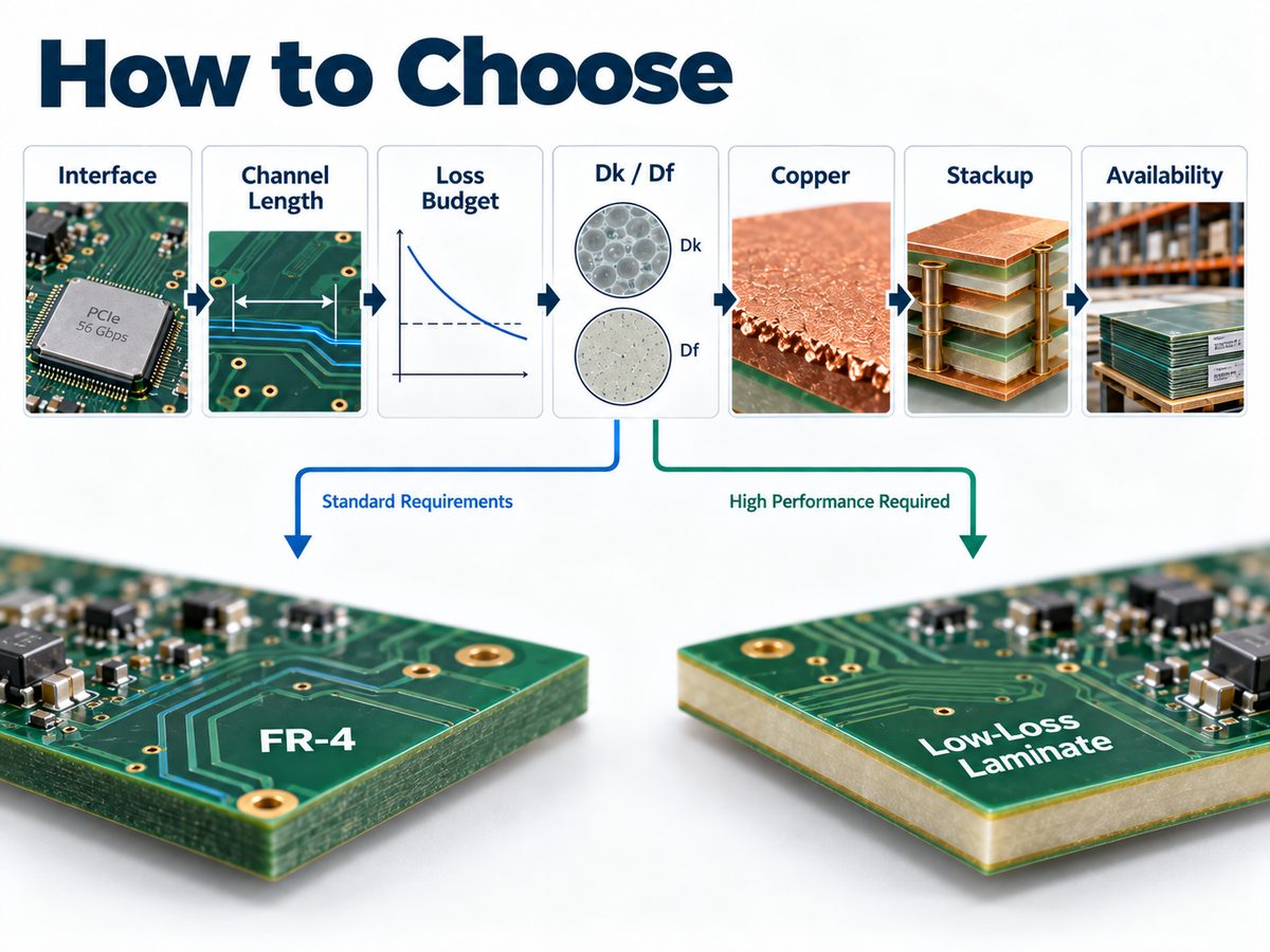
A practical selection process is:
- Identify the interface and data rate. Define whether the board uses PCIe, Ethernet, USB, HDMI, DDR, proprietary SerDes, RF, or a combination.
- Estimate the channel length. Include PCB traces, vias, connectors, cables, and backplane sections where applicable.
- Define the insertion-loss budget. Determine how much attenuation the transmitter and receiver can tolerate.
- Compare Dk and Df at relevant frequencies. Avoid comparing datasheet values measured with different methods without understanding the difference.
- Review copper foil type. Smoother copper can reduce conductor loss on long or high-frequency channels.
- Check dielectric thickness and glass style. These affect impedance geometry and differential skew.
- Confirm the production stackup. Make sure the required cores, prepregs, and copper options are actually available.
- Balance margin against cost. Use the material performance the channel requires rather than automatically specifying the lowest-loss laminate available.
For high-layer-count boards, a hybrid stackup may also be worth considering. Low-loss material can be used on critical signal layers while more conventional materials are used elsewhere, provided the laminate systems are compatible and the construction can be manufactured reliably.
Which High Speed PCB Design Guidelines Depend on Material Selection?
Several high-speed PCB design decisions depend directly on the material and stackup.
Controlled impedance is the most obvious example. A 50 Ω trace does not have one standard width. Its geometry depends on:
- dielectric constant
- dielectric thickness
- copper thickness
- solder mask
- reference-plane position
- whether the trace is microstrip or stripline
Material selection also affects differential-pair geometry and routing space under dense BGAs.
Via structures can also change with channel requirements. Long through-hole stubs may add resonances and loss, so designs may use:
- blind vias
- buried vias
- backdrilling
- controlled-depth drilling
Reference-plane continuity should remain intact. Crossing a split plane or poorly defined return path can create a larger signal-integrity problem than the laminate itself.
Other material-dependent checks include:
- stackup symmetry
- dielectric thickness tolerance
- resin content
- copper profile
- impedance tolerance
- trace-width manufacturability
- lamination compatibility
High-speed layout and stackup development should therefore happen together rather than as separate steps.
What Should You Confirm With a PCB Manufacturer Before Finalizing the Material?
Before freezing the layout, confirm the actual production construction with the PCB manufacturer.
At minimum, verify:
- exact laminate grade or approved equivalent
- core and prepreg construction
- finished dielectric thickness
- copper foil type
- starting and finished copper thickness
- Dk and Df reference values
- test frequency and measurement method
- glass style where relevant
- target impedance and tolerance
- permitted material substitutions
- material availability
- hybrid-material compatibility
- prototype and production lead time
For controlled-impedance boards, stackup review before layout release is especially useful. A change in dielectric thickness or copper thickness can require new trace widths or differential spacing.
EBest Circuit supports high-speed PCB fabrication and PCBA projects involving controlled impedance, multilayer stackups, HDI structures, low-loss laminates, RF materials, and mixed-material constructions. Our engineering team can review the proposed stackup, material availability, impedance requirements, via structure, copper specification, and manufacturing data before production.
Frequently Asked Questions About High-Speed PCB Materials
What is the best material for a high-speed PCB?
The best PCB material for high speed applications is the material that meets the channel loss and impedance targets without unnecessary cost or fabrication risk. The correct choice depends on data rate, trace length, insertion-loss budget, stackup, copper profile, operating environment, manufacturing requirements, and cost. Shorter channels may work well with enhanced FR-4, while longer loss-sensitive channels can justify low-loss or very-low-loss laminates.
Is FR-4 suitable for high-speed PCB design?
Yes. FR-4 can still be suitable for high-speed digital designs when channel length and insertion loss remain within the interface budget. The decision should be based on channel simulation or loss analysis rather than a fixed frequency threshold.
What Dk is suitable for a high-speed PCB?
Many high-speed PCB materials have Dk values roughly between 3 and 4.5, but the exact value is less important than predictable electrical behavior and a stackup that supports the required impedance geometry. Dk should also be compared using the same test method and frequency where possible.
Is lower Df always better for high-speed PCBs?
Electrically, lower Df generally reduces dielectric loss, but the lowest-Df material is not automatically the best commercial choice. Material cost, copper profile, availability, fabrication complexity, and actual channel length should also be considered.
When should I use a low-loss PCB laminate?
Low-loss material becomes more valuable when longer traces, higher SerDes rates, multiple connectors or vias, tighter eye margins, or demanding insertion-loss targets make standard FR-4 difficult to use reliably. The transition should be based on channel performance rather than a simple GHz threshold.
What information should I give my PCB manufacturer when selecting a high-speed material?
Provide the proposed stackup, laminate preference, dielectric thickness, copper weight, target impedance, impedance tolerance, interface type, expected data rate, critical trace lengths, via structure, and any insertion-loss requirement. If a specific material grade is mandatory, state whether substitutions are allowed.
If you are preparing a high-speed PCB or PCBA project, send your Gerber files, stackup, BOM, controlled-impedance requirements, and material specifications to sales@bestpcbs.com. EBest Circuit can review the material system, dielectric construction, copper profile, impedance targets, via structure, and manufacturing requirements before production, helping you avoid unnecessary material cost while protecting signal-integrity margin.