Co-Packaged Optics (CPO) is an optical interconnect architecture that places optical engines close to high-bandwidth chips such as switch ASICs, processors, and accelerators. By shortening the electrical path between the chip and the optical interface, CPO can reduce high-speed signal loss, lower I/O power, and support much higher bandwidth density than conventional front-panel pluggable optics.
CPO is moving from an emerging concept into real high-capacity networking hardware, driven particularly by AI data centers and hyperscale computing. For hardware engineers, this shift also changes how advanced packaging, thermal management, fiber routing, power delivery, PCB stackups, and system integration are approached.
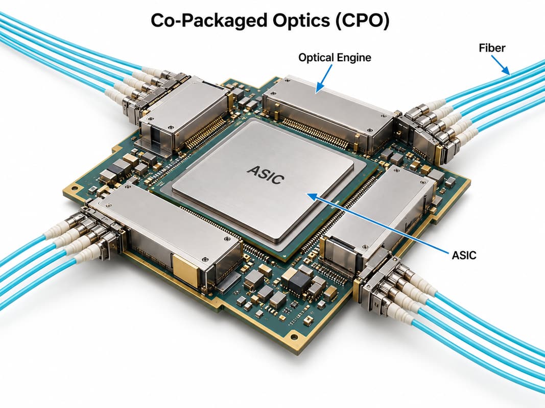
What Is Co-Packaged Optics (CPO)?
Co-Packaged Optics integrates optical engines within or immediately beside the package of a high-performance electronic chip, allowing high-speed electrical signals to travel only a short distance before being converted to light.
In a conventional pluggable-optics architecture, signals travel from the ASIC across the PCB to optical transceivers installed at the front panel. CPO moves this electrical-to-optical conversion much closer to the silicon.
The package can contain separate electronic and photonic dies rather than integrating every function onto one chip. CPO is therefore an optical and electronic integration architecture, not a single type of optical component.
How Does Co-Packaged Optics Work?
Co-Packaged Optics works by converting high-speed electrical data into optical signals close to the ASIC or processor and carrying the longer-distance portion of the link over fiber.
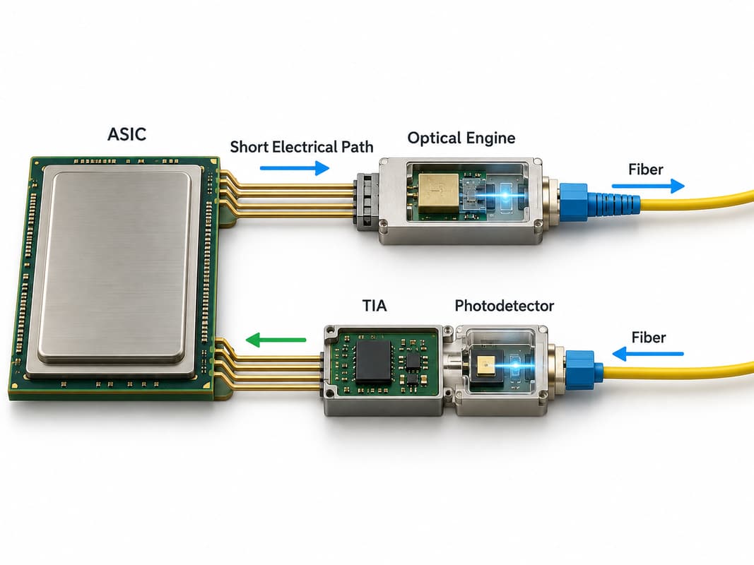
A typical transmit path is:
- The ASIC generates high-speed electrical data.
- A short electrical connection carries it to the optical engine.
- Driver electronics prepare the signal.
- A photonic integrated circuit modulates light with the data.
- Fiber carries the optical signal to another device.
The receive path reverses the process:
- Fiber delivers the incoming optical signal.
- A photodetector converts light into an electrical signal.
- A TIA and related electronics process the signal.
- The data reaches the ASIC over a short electrical connection.
Many CPO architectures use an external laser source (ELS). Light is generated away from the ASIC and delivered to the optical engine through fiber. OIF has standardized external-laser approaches for co-packaged optical systems through its ELSFP work, including field-replaceable laser modules.
What Technologies Make Co-Packaged Optics Possible?
CPO relies on silicon photonics, photonic integrated circuits, high-speed electronics, precision optical coupling, and heterogeneous integration working together.
Silicon photonics
Silicon photonics enables optical functions such as waveguides, modulators, couplers, and photodetectors to be fabricated in compact semiconductor-based devices.
Photonic integrated circuits
The PIC handles functions such as optical modulation, detection, routing, and coupling. Multiple optical channels can be integrated into one photonic engine to increase aggregate bandwidth.
High-speed electronic ICs
Drivers, TIAs, clocking circuits, and other interface electronics connect the optical section to the main ASIC.
External laser technology
Many architectures separate the laser from the optical engine to improve thermal conditions and serviceability.
Precision optical coupling
Fiber must be accurately aligned with the photonic interface. Small positional errors can increase coupling loss, so optical assembly requires much tighter mechanical control than ordinary board-level connectors.
These technologies provide the functional building blocks. Bringing them into one compact hardware platform is primarily an advanced-packaging task.
Co-Packaged Optics vs Pluggable Optics: What Is the Difference?
The main difference between Co-Packaged Optics and pluggable optics is the location of the optical engine: CPO places it close to the ASIC, while pluggable optics keeps the optical module at the system faceplate.
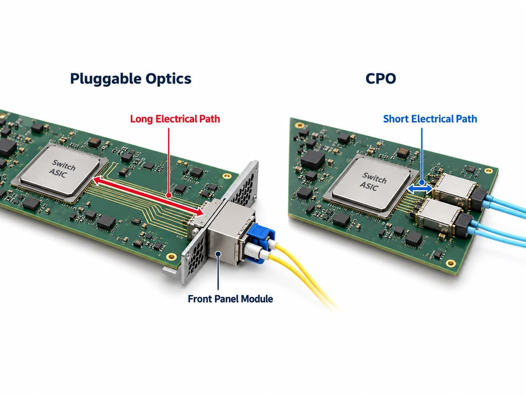
| Item | Pluggable Optics | Co-Packaged Optics |
|---|---|---|
| Optical engine location | Front panel | Close to ASIC |
| High-speed electrical path | Relatively long | Very short |
| PCB channel demand | Higher | Reduced near optical interface |
| Electrical loss | Higher at very high rates | Lower |
| Bandwidth density | Limited by faceplate space | Potentially much higher |
| Module replacement | Simple | More complex |
| Packaging | Mature and modular | Highly integrated |
| Thermal design | Module and ASIC more separated | Optics and ASIC interact closely |
| Deployment maturity | Widely established | Entering broader production |
Pluggable optics remains attractive because individual modules can be replaced or upgraded without disturbing the main switch package.
CPO trades some of that modularity for a shorter electrical path. The trade becomes more attractive as SerDes speed, channel loss, power consumption, and faceplate density become harder to scale.
Co-Packaged Optics vs NPO vs LPO: How Do They Compare?
CPO, NPO, and LPO mainly differ in how close the optical engine sits to the ASIC and how much electrical processing remains between the ASIC and optics.
| Architecture | Optical Location | Electrical Reach | Serviceability | Integration |
|---|---|---|---|---|
| Traditional pluggable | Front panel | Longest | High | Low |
| LPO | Front panel | Long | High | Low |
| NPO | Near ASIC | Short | Moderate | Medium |
| CPO | At or within ASIC package environment | Shortest | More difficult | Highest |
Linear Pluggable Optics (LPO) retains a front-panel optical module while simplifying the signal-processing chain to reduce DSP-related power.
Near-Packaged Optics (NPO) places the optical engine near the ASIC without integrating it as tightly into the package.
Co-Packaged Optics (CPO) moves optics closest to the ASIC and has the highest degree of integration.
As the optical engine moves closer to the ASIC, electrical reach generally falls, but package complexity and service requirements increase.
What Are the Main Benefits of Co-Packaged Optics?
The main CPO benefits are lower electrical channel loss, lower I/O power potential, greater bandwidth density, and better scalability at very high data rates.
They result mainly from shortening the ASIC-to-optics electrical path:
- Lower electrical loss: shorter high-speed connections introduce less attenuation.
- Lower I/O power potential: short channels can reduce the need for aggressive equalization, retimers, or additional signal conditioning.
- Higher bandwidth density: optical bandwidth is less dependent on the number of pluggable modules that fit on the front panel.
- Better bandwidth scaling: increasing ASIC bandwidth does not require every optical lane to traverse a long PCB channel.
- Less demanding ASIC-to-optics board routing: much of this interface moves toward the package.
These advantages become more valuable as per-lane data rate and total system bandwidth rise.
What Are the Main Challenges of Co-Packaged Optics?
The main CPO challenges are thermal management, optical alignment, package yield, testing, fiber attachment, laser delivery, serviceability, and standardization.
- Thermal management: high-power ASICs create a difficult environment for nearby optical devices.
- Optical alignment: fiber-to-photonic interfaces require precise positioning to maintain coupling efficiency.
- Package yield: one defective electronic or optical component can affect the value of a complex multi-die package.
- Testability: both electrical and optical functions need to be screened before and after integration.
- Fiber attachment: fiber arrays require repeatable alignment and adequate mechanical reliability.
- External laser delivery: optical power must reach the photonic engines with controlled loss.
- Serviceability: integrated optical engines are more difficult to replace than front-panel transceivers.
- Standardization: electrical, optical, laser, package, and management interfaces are still developing.
Standardization is already progressing. OIF has published a 3.2 Tb/s co-packaged module implementation agreement as well as external-laser implementation agreements for CPO systems.
Why Is Co-Packaged Optics Important for AI Data Centers?
Co-Packaged Optics is important for AI data centers because large accelerator clusters require rapidly increasing network bandwidth while power and electrical-channel loss become harder to control.
As AI clusters scale, several requirements rise together:
- GPU/XPU-to-GPU/XPU traffic
- switch capacity
- SerDes data rate
- bandwidth density
- network power consumption
CPO reduces the board-level electrical distance between the switching silicon and optics before moving the traffic onto fiber.
Commercial hardware now shows the scale involved. NVIDIA’s Spectrum-X Ethernet Photonics uses 200 Gb/s SerDes, and its SN6800 platform reaches 409.6 Tb/s total bandwidth. NVIDIA stated in May 2026 that Spectrum-X Ethernet Photonics CPO switches were in production as part of the Vera Rubin platform.
This makes CPO especially relevant to AI scale-up fabrics, scale-out networks, high-radix Ethernet, and other accelerator-heavy infrastructure.
Where Is Co-Packaged Optics Used Today?
CPO is already entering production in AI and hyperscale networking, while applications such as direct processor optical I/O and broader disaggregated computing remain at earlier stages of adoption.
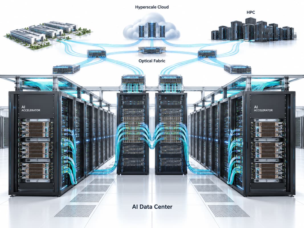
Current co-packaged optics applications include:
- AI data center networks: CPO connects very high-capacity switching silicon to optical fabrics used between accelerator systems.
- Hyperscale cloud networks: cloud operators face similar bandwidth-density and electrical-reach constraints as switch capacity increases.
- High-performance computing: large HPC systems require high-bandwidth communication between compute nodes.
- High-capacity Ethernet switching: switches are one of the clearest early commercial applications of CPO.
- Large routing platforms: high-throughput networking equipment can benefit when front-panel density and long electrical channels limit further scaling.
Commercialization is no longer hypothetical. Broadcom announced its 102.4 Tb/s Tomahawk 6–Davisson CPO Ethernet switch in 2025 as its third-generation CPO platform, while NVIDIA reported production of Spectrum-X Ethernet Photonics systems in 2026.
Emerging applications include:
- processor-to-processor optical I/O
- GPU and XPU optical interfaces
- chiplet-to-chiplet optical links
- disaggregated compute and memory systems
- future optical connections between separated compute resources
These emerging uses extend the same principle beyond network switching: convert data to light closer to the device when conventional electrical interconnect becomes inefficient in bandwidth, reach, or power.
How Does Advanced Packaging Support Co-Packaged Optics?
Advanced packaging supports CPO by placing electronic and photonic dies close enough to communicate over short, dense electrical connections while maintaining optical alignment and thermal control.
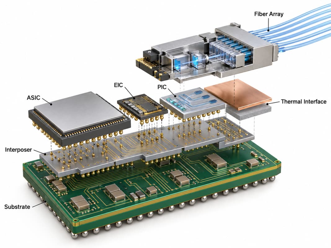
A CPO assembly may combine:
- switch or compute ASICs
- PICs
- electronic driver and receiver ICs
- optical engines
- organic package substrates
- silicon or organic interposers
- redistribution structures
- micro-bumps or other fine-pitch connections
- fiber coupling interfaces
- thermal interfaces
The packaging architecture must solve three problems at once:
- keep high-speed electrical interconnects short;
- maintain accurate optical coupling;
- provide an effective thermal path away from high-power silicon.
Depending on the platform, this may involve 2.5D integration, interposers, chiplets, fine-pitch redistribution, micro-bumps, or hybrid bonding.
How Does Co-Packaged Optics Change PCB and System Design?
CPO changes PCB design by moving some of the fastest ASIC-to-optics routing into the package while increasing the importance of board-level power delivery, dense breakout routing, thermal management, and mechanical integration.
The PCB still carries several critical responsibilities:
- Power delivery: high-power ASICs and supporting electronics require low-impedance power distribution.
- Remaining high-speed links: PCIe, memory, clocks, control, management, and other interfaces still need controlled signal integrity.
- BGA escape routing: large advanced packages can require dense multilayer breakout.
- Fiber-related mechanical layout: fiber exits, bend radius, connectors, cold plates, and heat sinks affect component placement.
- Thermal integration: package position, PCB copper, airflow, and cooling hardware influence the complete thermal path.
Long ASIC-to-optics board traces can be reduced, while power, remaining high-speed connections, cooling, mechanical clearances, and package breakout remain board-level design concerns.
What PCB Requirements Matter in Co-Packaged Optics Systems?
CPO systems typically need PCBs with controlled impedance, suitable low-loss materials, dense multilayer routing, robust power distribution, accurate dimensions, and support for large advanced packages.
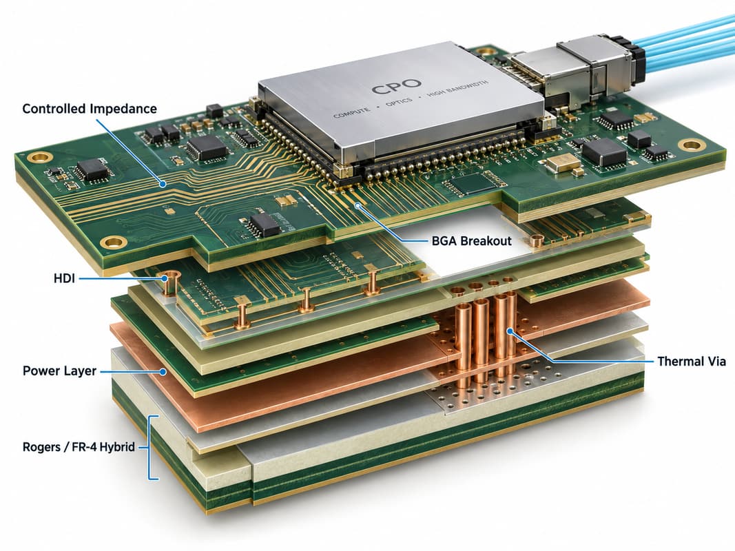
Typical requirements include:
- Low-loss laminate: for high-speed electrical links that remain on the board.
- Controlled impedance: for SerDes, PCIe, clocks, and other high-speed channels.
- HDI structures: microvias and sequential lamination may be needed for dense package breakout.
- High layer count: signal, power, and ground routing can require complex stackups.
- Power integrity: high-current ASICs need suitable planes, copper distribution, and via capacity.
- Fine-pitch BGA routing: large advanced packages can require tight trace and via geometry.
- Dimensional control: important around package, cooling, fiber, and connector interfaces.
- Thermal structures: thermal vias, copper planes, copper inlays, or other heat-spreading features may be required.
- Backdrilling: through-hole via stubs may need removal on sensitive high-speed channels.
- Surface finish: the finish should match the assembly and reliability requirements.
The PCB specification should come from the actual channel, package, power, and mechanical requirements rather than from a generic “CPO PCB” stackup.
What Should You Consider When Manufacturing PCBs for CPO Hardware?
When manufacturing PCBs for CPO hardware, the main concerns are material selection, impedance control, stackup repeatability, HDI capability, power delivery, dimensional accuracy, thermal requirements, and prototype-to-production consistency.
A useful RFQ package should include:
- PCB stackup
- laminate grade or loss target
- dielectric thickness
- finished board thickness
- copper weight
- controlled-impedance values and tolerance
- minimum trace and spacing
- via and microvia structure
- backdrill requirements
- BGA pitch
- dimensional tolerances
- thermal requirements
- surface finish
- assembly drawings
- prototype and production quantity
For high-speed channels, include the operating data rate and insertion-loss target when available.
At EBest Circuit, we bring more than 20 years of PCB and PCBA manufacturing experience to CPO-related hardware, with production capabilities in both China and Vietnam. We support low-loss multilayer PCBs, HDI, controlled impedance, fine-pitch BGA designs, advanced thermal structures, and complex stackups for high-speed systems where signal integrity, power delivery, and manufacturing consistency all matter.
Our advantage is not limited to board fabrication. For CPO and AI-related high-speed hardware, we have experience with Rogers materials such as RO4350B, RO4003C, RO3003, RO3010, and RT/duroid 5880, as well as Rogers/FR-4 hybrid multilayer constructions. We can combine material selection, controlled-impedance stackups, HDI routing, fine-pitch BGA breakout, thermal design, and PCBA in one manufacturing flow, supporting projects from prototype builds through volume production.
FAQs About Co-Packaged Optics
1. Is co-packaged optics the same as silicon photonics?
No. Silicon photonics is a technology used to create integrated optical components, while CPO is a system and packaging architecture that places optical engines close to high-performance electronic chips. Silicon photonics is one of the technologies that can enable CPO.
2. Will co-packaged optics replace pluggable optics?
Not completely. Pluggable optics offers strong serviceability, an established ecosystem, and simple replacement. CPO is more attractive where bandwidth density, electrical reach, and power become limiting factors. Both architectures are likely to coexist across different applications.
3. What is the difference between CPO and optical I/O?
CPO is a specific integration approach, while optical I/O is a broader concept. CPO commonly refers to optics integrated around switch or compute packages to replace longer electrical links. Optical I/O can also include direct optical interfaces on processors, accelerators, chiplets, and other semiconductor devices.
4. Why does CPO often use external lasers?
CPO often uses external lasers to separate the laser source from the hot ASIC environment. This can improve thermal conditions and simplify laser replacement. The optical engine receives laser light through fiber and uses that light for modulation.
5. Is co-packaged optics only used in AI data centers?
No. AI infrastructure is currently a major driver, but CPO can also support hyperscale cloud networks, HPC systems, high-capacity routers, telecom equipment, disaggregated computing, and emerging processor optical I/O.
6. What are the biggest barriers to CPO adoption?
The biggest barriers are manufacturing and integration complexity. Key issues include thermal management, packaging yield, optical alignment, fiber attach, manufacturing cost, test complexity, serviceability, laser architecture, and standardization.
7. Does CPO still require high-speed PCBs?
Yes. CPO shortens some of the highest-speed electrical paths, but the system still contains board-level high-speed links, power distribution, control interfaces, BGA routing, connectors, and other circuitry. PCB design remains an important part of the platform.
8. Which companies are developing co-packaged optics?
Leading co-packaged optics companies include Broadcom, NVIDIA, Marvell, Intel, Cisco, and Ayar Labs. The broader ecosystem also includes foundries, packaging companies, laser suppliers, fiber manufacturers, and optical-component suppliers working on different parts of the CPO platform.