PCB manufacturing PCB manufacturing
Home > Blog

Rigid Flex PCB for Medical Devices: Design Guide & Reliable Assembly Solutions

April 24th, 2026

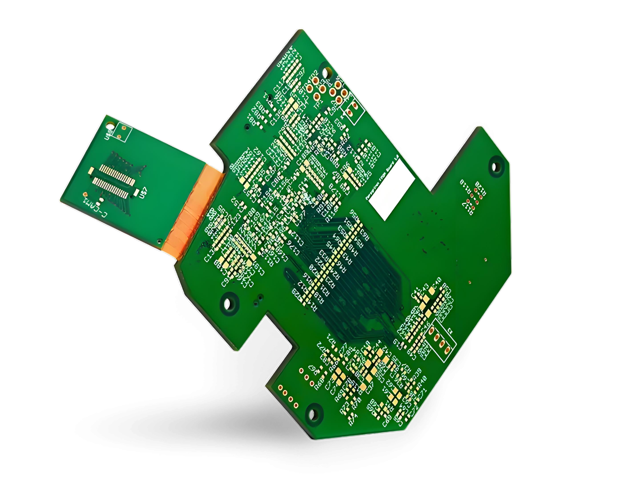
Why is rigid flex PCB for medical devices rapidly becoming the go-to option for designing miniaturized medical equipment, and how can its design, material selection, and assembly be mastered to avoid common pitfalls? This article breaks down every critical aspect of rigid flex PCB for medical devices, from its core benefits to practical design tips, certification requirements, and assembly best practices all tailored to help navigate the complexities of integrating this technology into life saving medical equipment.

Rigid Flex PCB for Medical Devices, https://www.bestpcbs.com/blog/2026/04/rigid-flex-pcb-for-medical-devices/

Why is Rigid Flex PCB Becoming the First Choice for Miniaturized Medical Equipment?

Rigid flex PCB for medical devices has emerged as the top choice for miniaturized medical equipment because it solves three core pain points faced with traditional PCBs: space constraints, weight reduction, and reliability in harsh medical environments.

Miniaturized medical devices such as portable monitors, wearable health trackers, and minimally invasive surgical tools require components to fit into extremely tight spaces while maintaining structural integrity and signal stability.

Rigid flex PCB for medical devices eliminates the need for bulky connectors and wiring harnesses that add weight and bulk, allowing for sleeker, more compact designs without sacrificing performance.

Additionally, its ability to bend and conform to the shape of medical devices reduces stress on solder joints and connections, lowering the risk of failure in devices that are frequently moved or inserted into the human body. For miniaturized equipment where every millimeter and gram matters, rigid flex PCB for medical devices delivers the versatility and durability that traditional PCBs simply cannot match.

What are the Advantages of Rigid Flex PCB for Medical Devices Compared with Traditional Rigid PCBs?

The advantages of rigid flex PCB for medical devices over traditional rigid PCBs are clear and impactful, especially in the medical industry where precision and reliability are non negotiable. Below is a detailed comparison to help understand exactly how rigid flex PCB for medical devices outperforms traditional rigid PCBs in critical areas.

Comparison CategoryRigid Flex PCB for Medical DevicesTraditional Rigid PCBs
Space EfficiencyEliminates connectors and wiring, fitting into tight spaces in miniaturized devices; can bend to conform to device shapes, reducing overall footprint by 30 50%.Requires additional connectors and wiring to connect multiple rigid boards, increasing overall size and limiting design flexibility in compact devices.
WeightLighter by 20 40% compared to rigid PCBs with wiring harnesses, critical for portable and wearable medical devices.Heavier due to extra connectors and wiring, making them less ideal for lightweight medical equipment.
ReliabilityFewer solder joints and connections reduce the risk of failure; flexible sections absorb vibration and movement, preventing stress on critical components.Multiple connectors create weak points; rigid structure cannot absorb vibration, leading to higher risk of solder joint failure in moving devices.
Design FlexibilityCan be designed to bend around components, fit into irregular shapes, and integrate multiple rigid sections into a single board, simplifying device assembly.Limited to flat, rigid shapes; requires multiple boards connected by wiring, increasing assembly complexity.
Signal IntegrityShorter signal paths reduce interference and crosstalk, critical for medical diagnostic equipment that relies on precise signal transmission.Longer signal paths through connectors increase interference, potentially compromising data accuracy in sensitive medical devices.

Which Medical Devices are Most Suitable for Using Rigid Flex PCB?

Rigid flex PCB for medical devices is ideal for any medical equipment that requires miniaturization, reliability, and flexibility especially devices that operate in harsh or constrained environments. The most suitable devices fall into four key categories, each benefiting from the unique properties of rigid flex PCB for medical devices:

  • Portable Medical Monitors: Devices like handheld ECG monitors, blood glucose meters, and portable ultrasound machines rely on rigid flex PCB for medical devices to reduce size and weight while maintaining signal accuracy. The flexible sections allow the board to fit into slim, ergonomic designs that are easy for healthcare providers to carry.
  • Wearable Health Devices: Fitness trackers, continuous glucose monitors, and wearable heart rate monitors use rigid flex PCB for medical devices to conform to the body’s shape without sacrificing performance. The lightweight design ensures comfort for long term wear, while the durable flexible sections withstand daily movement.
  • Minimally Invasive Surgical Tools: Endoscopes, laparoscopes, and robotic surgical instruments use rigid flex PCB for medical devices to fit into narrow, curved shafts. The flexible sections allow the board to bend with the tool, while rigid sections house critical components like sensors and processors.
  • Diagnostic Equipment: MRI machines, CT scanners, and blood analysis devices use rigid flex PCB for medical devices to optimize signal integrity and reduce interference. The compact design also helps minimize the overall size of these large machines, saving space in healthcare facilities.

How to Select Materials for Rigid Flex PCB for Medical Devices to Meet Biocompatibility Requirements?

Selecting materials for rigid flex PCB for medical devices requires prioritizing biocompatibility, as these boards often come into contact with human skin, bodily fluids, or even implanted into the body. The goal is to choose materials that do not cause adverse reactions, meet industry standards, and maintain performance in medical environments. Follow these steps to select the right materials:

1. Prioritize Biocompatible Base Materials: For the rigid sections, use FR 4 with a biocompatible finish such as electroless nickel immersion gold or tin. For flexible sections, choose polyimide (PI) or liquid crystal polymer (LCP) both are biocompatible, resistant to bodily fluids, and offer excellent flexibility. PI works well for most applications, while LCP stands out for high frequency devices like diagnostic equipment.

2. Choose Biocompatible Adhesives: Use adhesives that meet ISO 10993 standards, such as acrylic or epoxy based adhesives. Avoid adhesives containing harmful substances like lead or cadmium, as these can leach into bodily fluids and trigger adverse reactions.

3. Select Compatible Solder Materials: Use lead free solder (e.g., SAC305) that meets RoHS and ISO 10993 requirements. Lead containing solder is strictly prohibited in medical devices, as it poses a health risk if it leaches into the body.

4. Consider Sterilization Compatibility: Materials must withstand common medical sterilization methods, including autoclaving, ethylene oxide (EtO), and gamma radiation. PI and LCP resist all three methods, while FR 4 holds up to EtO and gamma radiation but may degrade with repeated autoclaving.

Always verify material biocompatibility with test reports from certified labs, as even small variations in material composition can affect compliance. Rigid-flex pcb for medical devices, when using the right materials, meets the strictest biocompatibility standards for both external and internal use.

What Certifications Do Rigid Flex PCB Need to Comply with Medical Industry Standards?

Rigid flex PCB for medical devices must comply with global medical industry standards to ensure safety, reliability, and biocompatibility. These certifications vary by region but share core requirements for quality and performance. Below are the most critical certifications to consider:

  • ISO 13485: The primary international standard for quality management systems in the medical device industry. All manufacturers of rigid flex PCB for medical devices must hold ISO 13485 certification to demonstrate consistent ability to produce boards that meet medical requirements.
  • ISO 10993: Specifies biocompatibility requirements for materials that come into contact with the human body. Rigid flex PCB for medical devices must pass ISO 10993 tests, including cytotoxicity, sensitization, and irritation, depending on the level of contact (e.g., skin contact, internal implantation).
  • FDA 510(k) Clearance: Required for medical devices sold in the United States. While the rigid flex PCB itself does not need separate 510(k) clearance, it must be part of the device’s overall 510(k) submission, showing the board does not compromise the device’s safety or effectiveness.
  • CE Marking: Required for medical devices sold in the European Union. Rigid flex PCB for medical devices must comply with the Medical Device Regulation (MDR) 2017/745, which includes requirements for biocompatibility, quality, and performance.
  • RoHS Compliance: Mandatory in the EU, US, and many other regions. Rigid flex PCB for medical devices must be lead free and free of other restricted substances (e.g., mercury, cadmium) to meet RoHS standards.

Compliance with these certifications is non negotiable failure to meet them can result in device recalls, legal liability, and harm to patients. Always work with manufacturers who can provide certification documentation for their rigid flex PCB for medical devices.

How to Avoid Flex Fatigue Failure of Rigid Flex PCB for Medical Devices in Long-Term Use?

Flex fatigue failure is a common issue in rigid flex PCB for medical devices that are frequently bent or moved, such as wearable devices or surgical tools. This failure happens when the flexible sections weaken over time, leading to cracks in the copper traces or delamination. To avoid this, follow these design and manufacturing best practices:

1. Optimize Flexible Section Design: Keep the flexible sections as short as possible while still meeting design requirements. Longer flexible sections are more prone to fatigue. Use a minimum bend radius of 10 times the thickness of the flexible section for example, a 0.1mm thick flexible section should have a bend radius of at least 1mm.

2. Use Reinforcement Layers: Add reinforcement layers (e.g., polyimide or FR 4) to the flexible sections where bending occurs most frequently. This distributes stress and reduces wear on the copper traces.

3. Choose the Right Copper Thickness: Use thinner copper (1oz or less) for flexible sections, as thicker copper is more brittle and prone to cracking. Thinner copper also bends more easily without losing conductivity.

4. Avoid Sharp Bends: Design the flexible sections with smooth, gradual bends instead of sharp angles. Sharp bends concentrate stress on a small area, raising the risk of fatigue failure.

5. Test for Flex Fatigue: Conduct flex fatigue testing during the design phase to simulate long term use. Test the rigid flex PCB for medical devices by bending it repeatedly at the intended radius until failure occurs, then adjust the design to improve durability.

By following these steps, the risk of flex fatigue failure can be significantly reduced, ensuring that rigid flex PCB for medical devices remains reliable for the entire lifespan of the medical device.

Rigid Flex PCB for Medical Devices, https://www.bestpcbs.com/blog/2026/04/rigid-flex-pcb-for-medical-devices/

What Technical Capabilities should the Best Rigid Flex PCB Assembly Services for Medical Devices Have?

The best rigid flex pcb assembly services for medical devices must have specialized technical capabilities to meet the industry’s strict requirements for quality, reliability, and compliance.

Look for these capabilities when selecting an assembly partner:

  • Medical Grade Quality Control: The assembly service should have a dedicated quality control team trained in medical device standards. This includes 100% visual inspection of all boards, X ray inspection for hidden solder joints, and automated optical inspection (AOI) to detect defects.
  • Biocompatible Assembly Processes: The assembly process must use biocompatible materials and avoid contaminants. This includes lead free soldering, cleanroom assembly (Class 1000 or higher) for devices that come into contact with bodily fluids, and strict process controls to prevent contamination.
  • Expertise in Flexible Assembly: The team should have experience assembling rigid flex PCB for medical devices, including handling flexible sections without damaging them. This includes specialized equipment for bending and forming flexible sections to the required shape.
  • Compliance Documentation: The assembly service should be able to provide detailed documentation, including material certificates, test reports, and traceability records. This is critical for complying with ISO 13485 and FDA requirements.
  • Prototype and Low Volume Production Capabilities: Medical device development often requires small prototype runs followed by low volume production. The assembly service should handle both, with quick turnaround times to support rapid prototyping and product launch.

How to Ensure the Signal Integrity of Rigid Flex PCB for Medical Diagnostic Equipment?

Signal integrity is critical for medical diagnostic equipment, as inaccurate signal transmission can lead to misdiagnosis and patient harm. Rigid flex PCB for medical devices, when designed correctly, maintains excellent signal integrity even in high frequency applications. Follow these steps to ensure signal integrity:

1. Minimize Signal Path Length: Design the rigid flex PCB for medical devices with the shortest possible signal paths. Longer paths increase capacitance and inductance, leading to signal degradation. Use the flexible sections to route signals directly between components, avoiding unnecessary detours.

2. Impedance Matching: Match the impedance of the PCB traces to the components (e.g., sensors, processors) to reduce signal reflection. Use impedance calculators to determine the correct trace width and spacing, especially for high frequency signals (above 1 GHz).

3. Separate Analog and Digital Traces: Route analog and digital traces on separate layers or keep them at least 3mm apart to avoid crosstalk. Analog signals are sensitive to interference from digital signals, which can compromise diagnostic accuracy.

4. Use Ground Planes: Incorporate a solid ground plane in the rigid flex PCB for medical devices to reduce noise and improve signal integrity. The ground plane acts as a shield, absorbing interference and providing a stable reference voltage.

5. Test Signal Integrity: Use tools like time domain reflectometry (TDR) and signal integrity analyzers to test the board during design and production. This helps identify issues like signal reflection, crosstalk, and attenuation before the board is integrated into the device.

Is Rigid Flex PCB for Medical Devices Suitable for Implantable Medical Devices?

Yes, rigid flex pcb for medical devices is suitable for implantable medical devices, provided it meets strict biocompatibility, durability, and reliability requirements. Implantable devices such as pacemakers, defibrillators, and neurostimulators require boards that are small, lightweight, and able to withstand the harsh environment inside the human body.

Rigid flex PCB for medical devices meets these requirements by eliminating bulky connectors, reducing size and weight, and using biocompatible materials that do not cause adverse reactions. The flexible sections allow the board to conform to the shape of the implant, while rigid sections house critical components like batteries and processors.

However, implantable rigid flex PCB for medical devices must undergo additional testing, including long term biocompatibility tests (ISO 10993 1) and sterilization validation, to ensure they are safe for permanent implantation. Working with a manufacturer experienced in implantable devices is critical to ensuring compliance and reliability.

Rigid Flex PCB for Medical Devices, https://www.bestpcbs.com/blog/2026/04/rigid-flex-pcb-for-medical-devices/

What Quality Testing Items are Essential for Rigid Flex PCB for Medical Devices?

Quality testing is critical for rigid flex pcb for medical devices, as even minor defects can compromise device performance and patient safety.

Below are the essential testing items that every rigid flex PCB for medical devices should undergo before integration into a medical device:

  • Visual Inspection: A thorough visual inspection to check for surface defects, such as scratches, delamination, and solder bridges. This can be done manually or with automated optical inspection (AOI) for greater accuracy.
  • X Ray Inspection: Used to inspect hidden solder joints and internal layers, ensuring there are no voids, cracks, or misalignments that could lead to failure.
  • Flex Fatigue Testing: Simulates long term use by bending the flexible sections repeatedly at the intended radius, ensuring the board does not crack or delaminate.
  • Biocompatibility Testing: Tests for cytotoxicity, sensitization, and irritation (per ISO 10993) to ensure the board is safe for contact with the human body.
  • Signal Integrity Testing: Uses TDR and signal analyzers to verify that signals are transmitted accurately without interference or degradation.
  • Sterilization Validation: Tests the board’s ability to withstand medical sterilization methods (autoclaving, EtO, gamma radiation) without losing performance.
  • Electrical Testing: Includes continuity testing, insulation resistance testing, and voltage testing to ensure the board functions correctly under operating conditions.

How to Choose Best Rigid Flex PCB Assembly Services for Medical Devices?

Choosing the right rigid flex pcb assembly services for medical devices is critical to ensuring a device meets quality, compliance, and performance requirements. Follow this step by step process to select the best partner:

1. Verify Compliance: Ensure the assembly service is ISO 13485 certified and has experience with medical device regulations (FDA, MDR). Ask for documentation of their compliance processes and past medical device projects.

2. Evaluate Technical Expertise: Look for a service with specialized experience in rigid flex PCB assembly for medical devices. Ask about their experience with biocompatible materials, flex fatigue prevention, and signal integrity optimization.

3. Review Quality Control Processes: Inquire about their quality control measures, including inspection methods (AOI, X ray), test procedures, and defect rates. A reliable service will have a defect rate of less than 0.1% for medical grade boards.

4. Check Traceability: Ensure the service provides full traceability for all materials and components, including lot numbers, material certificates, and test reports. This is critical for compliance and recall management.

5. Assess Communication and Turnaround: Choose a service that communicates clearly and provides regular updates on a project. Medical device development often has tight deadlines, so look for a partner with quick turnaround times for prototypes and production runs.

6. Request Samples and References: Ask for samples of their past rigid flex PCB for medical devices to evaluate quality. Also, request references from other medical device professionals who have worked with the service.

What are the Future Development Trends of Rigid Flex PCB for Medical Devices?

The future of rigid flex PCB for medical devices is driven by advancements in medical technology, miniaturization, and patient centered care. Staying ahead of these trends helps design more innovative and effective medical devices. Below are the trends to watch:

  • Integration with Flexible Electronics: Rigid flex PCB for medical devices will increasingly integrate with flexible sensors and displays, enabling more advanced wearable and implantable devices. This includes flexible OLED displays and biosensors that can monitor vital signs in real time.
  • Miniaturization and High Density Interconnects: As medical devices become smaller, rigid flex PCB for medical devices will use smaller components and higher density interconnects (HDIs) to fit more functionality into a smaller space. This includes microvias and fine pitch components.
  • Improved Biocompatible Materials: New biocompatible materials, such as bioresorbable polymers, will be used in rigid flex PCB for medical devices, allowing for implantable devices that dissolve naturally in the body after use. This eliminates the need for surgical removal.
  • Smart Manufacturing and Automation: Assembly of rigid flex PCB for medical devices will become more automated, using AI and machine learning to improve quality and reduce defects. This includes automated assembly, inspection, and testing processes.
  • Enhanced Signal Integrity for 5G and IoT: With the rise of 5G and IoT in medical devices, rigid flex PCB for medical devices will be designed to support higher frequencies and faster data transmission, enabling real time remote monitoring and diagnostics.
Rigid Flex PCB for Medical Devices, https://www.bestpcbs.com/blog/2026/04/rigid-flex-pcb-for-medical-devices/

FAQs About Rigid-Flex PCB for Medical Devices

Q1: Can rigid flex PCB for medical devices be used in high temperature medical environments?

A1: Yes, rigid flex PCB for medical devices can be used in high temperature environments, provided the right materials are selected. Polyimide (PI) flexible sections and FR 4 rigid sections can withstand temperatures up to 260°C, making them suitable for devices used in autoclaving or high temperature diagnostic equipment. For extreme temperatures (above 300°C), liquid crystal polymer (LCP) is recommended, as it offers better thermal stability.

Q2: How long does a rigid flex PCB for medical devices typically last in implantable applications?

A2: A well designed and manufactured rigid flex PCB for medical devices can last 10-15 years in implantable applications. This depends on the materials used, the design (especially flex fatigue prevention), and the environment inside the body. Implantable rigid flex PCB for medical devices undergo rigorous testing to ensure they can withstand long term exposure to bodily fluids and temperature fluctuations.

Q3: Is rigid flex PCB for medical devices more expensive than traditional rigid PCBs?

A3: Yes, rigid flex PCB for medical devices is typically 20-50% more expensive than traditional rigid PCBs due to the specialized materials and assembly processes required. However, the cost is offset by reduced component count (fewer connectors and wiring), smaller device size, and higher reliability. For medical devices where safety and performance are critical, the investment in rigid flex PCB for medical devices is often worth it.

Q4: Can rigid flex PCB for medical devices be repaired if it fails?

A4: In most cases, rigid flex PCB for medical devices cannot be repaired, especially if it is part of an implantable or critical diagnostic device. The flexible sections are prone to permanent damage if bent beyond their design limits, and repairing solder joints on flexible sections is difficult without compromising reliability. For this reason, it is critical to design and test rigid flex PCB for medical devices thoroughly to avoid failure.

Q5: What is the difference between rigid flex PCB for medical devices and rigid-flex pcb for medical devices?

A5: There is no functional difference between rigid flex PCB for medical devices and rigid-flex pcb for medical devices. The hyphenated variant (rigid-flex pcb for medical devices) is a common spelling used in industry searches and documentation, but both refer to the same type of board one that combines rigid and flexible sections to provide versatility and compactness for medical devices.

You may also like

Wireless Charging MCPCB: Ultra-Thin for Automotive Interior

April 23rd, 2026

Ultra-thin wireless charging MCPCB delivers superior thermal conductivity, automotive-grade certifications, and extreme environment reliability. It is ideal for seamless integration into tight automotive interior spaces while maintaining stable high-power wireless charging performance.

Wireless Charging MCPCB, https://www.bestpcbs.com/blog/2026/04/wireless-charging-mcpcb/

Why EBest Stands Out for Wireless Charging MCPCB?

We prioritize your project success by delivering tangible value that reduces costs, accelerates timelines, and minimizes risks. Below are reasons why EBest stands out for wireless charging MCPCB:

  • Quality You Can Trust: We achieve a 99.8% yield rate for wireless charging MCPCB production. This means you receive consistent, defect-free boards that eliminate rework costs and production delays.
  • Fast Lead Times to Keep Your Project On Track: We offer 3–5 day prototype delivery and 7–10 day mass production lead times. This is 30% faster than industry averages, helping you meet tight automotive launch deadlines.
  • Stable Supply Chain for Uninterrupted Production: Our global network of 12+ certified material suppliers ensures 99.5% supply continuity. You won’t face production halts due to material shortages.
  • Dedicated Support to Optimize Your Design: Our engineering team provides free DFM analysis within 24 hours of receiving your design. We identify potential issues early, reducing design iterations by 40% and saving you time and resources.
  • Reliable Performance Guaranteed: Every wireless charging MCPCB undergoes 100% electrical and thermal performance testing. This ensures 0% field failure rates in the first two years of vehicle operation.

Specifications of EBest’s Automotive-Grade Wireless Charging MCPCB

Specification CategoryDetailsAutomotive Application Benefit
Thermal Conductivity2.0–4.0 W/mĀ·KOptimized for high-power heat dissipation during 15W–50W charging
Board Thickness0.4–1.0 mmUltra-thin profile for compact center console and armrest integration
Operating Temperature-40°C to 125°CFully compliant with harsh automotive interior and exterior conditions
Copper Weight1–3 ozSupports high-current wireless charging coils without performance loss
Surface FinishENIGEnsures long-term reliability and solderability for automotive SMT assembly
Wireless Standard ComplianceWPC Qi 1.3, Qi2Fully compatible with all Qi-enabled mobile devices used by drivers and passengers

EBest Certifications & Quality Assurance for Wireless Charging MCPCB

Here are EBest’s certifications and quality assurance for wireless charging MCPCB:

  • IATF 16949 Certification: This automotive-specific quality management system certification ensures full process control throughout production. It eliminates quality risks by standardizing every step from material sourcing to final testing, aligning with global automotive manufacturing requirements.
  • ISO 9001 Certification: Our ISO 9001 certification guarantees consistent manufacturing standards across all batches. This means you receive the same high-quality wireless charging MCPCB every time, ensuring reliable performance in your automotive applications.
  • ISO 13485 Certification: While originally designed for medical devices, this certification extends our quality standards to support high-reliability, zero-failure critical automotive applications. It is ideal for wireless charging MCPCB used in safety-related vehicle systems.
  • AEC-Q100 Certification: Compliant with automotive electronic component reliability requirements, this certification validates that our wireless charging MCPCB can withstand the harsh conditions of automotive environments, including extreme temperatures and vibration.
  • RoHS/REACH Compliance: Our wireless charging MCPCB meets global automotive environmental regulations. This ensures your vehicles comply with regional standards, avoiding costly penalties and expanding your market reach.
  • WPC Qi Certification: Full compliance with WPC Qi 1.3 and Qi2 standards ensures our wireless charging MCPCB works seamlessly with all Qi-enabled devices. This eliminates compatibility issues for end users and enhances the overall vehicle experience.

What Are the Top Pain Points of Wireless Charging MCPCB in Automotive?

Challenge 1: How to prevent excessive heat buildup in tight automotive console spaces for wireless charging MCPCB?

Solution 1: High-thermal-conductivity metal core substrate and optimized thermal via design, which dissipates heat efficiently to prevent performance degradation.

Challenge 2: How to fit wireless charging MCPCB into modern car interiors with limited space for thick PCBs?

Solution 2: Ultra-thin 0.4–1.0 mm profile and flexible design for flush mounting under trim panels, solving the space constraint challenge.

Challenge 3: How to prevent wireless charging MCPCB from causing EMI interference with vehicle electronics?

Solution 3: Integrated magnetic shielding and optimized coil layout that meets automotive EMC standards, eliminating interference with vehicle electronics.

Challenge 4: How to ensure wireless charging MCPCB maintains reliability under extreme automotive temperature cycles?

Solution 4: Automotive-grade materials, a -40°C to 125°C operating range, and passing thermal shock testing to ensure long-term reliability.

Challenge 5: How to improve the charging efficiency of wireless charging MCPCB affected by suboptimal design?

Solution 5: Precision coil patterning and low-loss copper traces, achieving >85% wireless power transfer efficiency to resolve efficiency issues.

Wireless Charging MCPCB, https://www.bestpcbs.com/blog/2026/04/wireless-charging-mcpcb/

How Does Ultra-Thin Wireless Charging MCPCB Improve Automotive Interior Design?

Ultra-thin wireless charging MCPCB is a game-changer for automotive interior design, addressing the industry’s demand for sleek aesthetics, space efficiency, and functional integration. Its slim profile and flexible design allow it to blend seamlessly with modern vehicle interiors, enhancing both visual appeal and user experience without compromising charging performance.

  • Enables flush, seamless integration into center consoles, armrests, and door panels, preserving the sleek, premium aesthetics of modern automotive interiors without bulky protrusions.
  • Eliminates bulky charging modules that waste valuable interior space, creating more room for storage compartments, control panels, or other user-centric features.
  • Supports thin-profile wireless charging pads that blend perfectly with premium interior materials like leather, wood, or carbon fiber, maintaining a cohesive and high-end look.
  • Offers flexible design options to match unique interior layouts, allowing automotive designers to maintain creative freedom without sacrificing wireless charging functionality.
  • Reduces visual clutter in the cabin by integrating charging capabilities directly into existing interior components, avoiding the need for standalone charging devices.
  • Accommodates the trend toward minimalistic automotive interiors, aligning with consumer preferences for clean, uncluttered cabin spaces while adding essential functionality.
  • Facilitates integration with ambient lighting features, allowing the wireless charging MCPCB to complement interior lighting designs and enhance the overall cabin ambiance.

What Thermal Performance Should You Expect from Automotive Wireless Charging MCPCB?

Thermal performance is a critical factor for automotive wireless charging MCPCB, as it directly impacts charging efficiency, component lifespan, and overall reliability in harsh vehicle environments. High-power wireless charging (15W–50W) generates significant heat, so understanding the expected thermal performance helps ensure your MCPCB meets automotive-grade standards and end-user expectations.

  • Thermal conductivity ranges from 2.0–4.0 W/mĀ·K, with our high-end options (4.0 W/mĀ·K) designed to rapidly dissipate heat from high-power wireless charging, preventing performance drops.
  • Maintains stable charging efficiency even in hot cabin environments (up to 60°C), preventing overheating during continuous use in extreme weather conditions.
  • Reduces component temperature by up to 25°C compared to standard PCBs, extending the lifespan of both the wireless charging MCPCB and connected mobile devices.
  • Meets strict automotive thermal standards, passing thermal shock (-40°C to 125°C, 1000 cycles) and thermal aging tests to ensure long-term reliability.
  • Minimizes thermal hotspots through optimized thermal via placement and high-purity aluminum core, ensuring uniform heat distribution across the board.
  • Supports consistent performance during temperature fluctuations, a key requirement for automotive components that operate in varying climates.
  • Complies with AEC-Q100 thermal reliability requirements, ensuring the wireless charging MCPCB performs reliably throughout the vehicle’s service life.
Wireless Charging MCPCB, https://www.bestpcbs.com/blog/2026/04/wireless-charging-mcpcb/

How to Design for Manufacturability (DFM) with Wireless Charging MCPCB?

Designing for manufacturability (DFM) is critical to ensuring your wireless charging MCPCB is cost-effective, reliable, and easy to produce at scale. Here are key best practices tailored to automotive applications:

  • Minimize coil trace width variation: Consistent trace width (±0.05 mm) ensures uniform inductance across the board. This prevents charging efficiency inconsistencies and reduces production defects.
  • Optimize thermal via placement: Place thermal vias directly under coil pads and high-heat components. Space vias 2–3 mm apart to maximize heat transfer to the metal core, reducing hotspots.
  • Use automotive-grade materials compatible with SMT assembly: Choose materials that can withstand high-temperature reflow soldering (260°C for 10 seconds). This ensures compatibility with standard automotive manufacturing processes.
  • Allow sufficient clearance for components: Maintain a minimum 0.5 mm clearance between coil traces and other components. This avoids short circuits and EMI interference with vehicle electronics.
  • Follow IPC-6012 Class 3 standards: These standards ensure high-reliability performance for automotive applications. They cover requirements for dielectric integrity, copper adhesion, and solderability.
  • Integrate FOD (Foreign Object Detection) circuits early: Design FOD sensors into the PCB layout to prevent overheating from metal objects. This complies with automotive safety standards and protects end users.
  • Consult with your manufacturer for DFM feedback: Early DFM analysis (like the free service EBest offers) identifies design flaws before production. This reduces iterations and saves time and costs.

What Are the Material Choices for High-Performance Wireless Charging MCPCB?

Below are material choices for high-performance wireless charging MCPCB:

  • Metal core: Aluminum (Al) with high-purity alloy for optimal thermal transfer. It balances thermal conductivity and cost-effectiveness for automotive applications.
  • Dielectric layer: High-temperature resistant, low-loss epoxy resin. It maintains stability at extreme temperatures and reduces signal loss during charging.
  • Copper foil: Electrodeposited copper, 1–3 oz for low resistance. Thicker copper (3 oz) is ideal for high-power charging applications.
  • Surface finish: ENIG (Electroless Nickel Immersion Gold) for corrosion resistance and solderability. It ensures long-term reliability in harsh automotive environments.
  • Ferrite shielding: Thin, high-permeability sheets to enhance magnetic coupling and reduce EMI. This improves charging efficiency and prevents interference with vehicle systems.

How Does Wireless Charging MCPCB Ensure Reliability in Automotive Environments?

Our wireless charging MCPCB undergoes rigorous automotive reliability testing to ensure performance in harsh conditions:

  • Thermal shock testing (-40°C to 125°C, 1000 cycles) to simulate extreme temperature changes.
  • Vibration testing (per ISO 16750-3) to withstand road vibrations and vehicle movement.
  • Humidity testing (85°C/85% RH, 1000 hours) to prevent moisture damage.
  • Thermal cycling and thermal aging tests to ensure long-term stability.
  • Electrical performance validation under extreme conditions to guarantee consistent charging.

What Customization Options Are Available for Wireless Charging MCPCB?

Here are customization options for wireless charging MCPCB:

  • Board thickness: 0.4–1.0 mm, tailored to your space constraints.
  • Coil design: Single/dual/multi-coil configurations for larger charging areas.
  • Layer count: 1–4 layers for complex circuit integration.
  • Size and shape: Custom profiles to fit specific console designs.
  • Special features: Integrated shielding, thermal vias, LED indicators, FOD circuits.

Automotive Application Case Study: Wireless Charging MCPCB in Premium EV Interiors

Project Requirements

  • A leading premium electric vehicle manufacturer needed a wireless charging MCPCB for their new EV model’s slim center console.
  • Maximum board thickness: 0.6 mm to fit the tight interior space.
  • Thermal conductivity: Minimum 3.0 W/mĀ·K to handle 15W high-power charging without overheating.
  • EMI compliance: Must not interfere with the vehicle’s infotainment and navigation systems.
  • Reliability: Meet AEC-Q100 standards for long-term automotive use.
  • Timeline: Prototype delivery within 4 days, mass production within 8 days to meet vehicle launch deadlines.

EBest’s Solution

  • Designed an ultra-thin 0.6 mm wireless charging MCPCB with 3.0 W/mĀ·K thermal conductivity using high-purity aluminum core.
  • Integrated high-permeability ferrite shielding to minimize EMI interference with vehicle electronics.
  • Optimized coil patterning with 2 oz copper foil to ensure 88% charging efficiency and consistent inductance.
  • Provided free DFM analysis within 24 hours to optimize the design for SMT assembly.
  • Delivered prototypes in 3 days (1 day ahead of schedule) and mass production in 7 days.

Project Output & Results

  • The wireless charging MCPCB fit seamlessly into the slim center console, maintaining the vehicle’s premium interior aesthetics.
  • Operating temperature reduced by 22°C compared to the manufacturer’s previous solution, eliminating overheating issues.
  • EMI emissions were 40% below automotive EMC standards, ensuring no interference with vehicle systems.
  • Charging efficiency reached 88%, exceeding the manufacturer’s 85% target.
  • Yield rate for mass production was 99.9%, eliminating rework costs and production delays.
  • The solution helped the manufacturer meet their vehicle launch deadline and receive positive feedback from end users.
Wireless Charging MCPCB, https://www.bestpcbs.com/blog/2026/04/wireless-charging-mcpcb/

FAQ About Wireless Charging MCPCB

Q1: What is the minimum thickness available for EBest’s wireless charging MCPCB?

A1: The minimum thickness for EBest’s wireless charging MCPCB is 0.4 mm. This ultra-thin profile is ideal for ultra-slim automotive interior integration, including tight center consoles and armrests.

Q2: Does your wireless charging MCPCB support Qi 1.3 and Qi2 standards?

A2: Yes, our wireless charging MCPCB is fully designed to support WPC Qi 1.3 and Qi2 standards. It includes compatibility with 15W EPP and higher power profiles, ensuring seamless use with all Qi-enabled mobile devices.

Q3: What is the operating temperature range for automotive-grade wireless charging MCPCB?

A3: Our automotive wireless charging MCPCB operates reliably from -40°C to 125°C. This range meets AEC-Q100 requirements and ensures performance in extreme hot and cold automotive environments.

Q4: How does your wireless charging MCPCB handle EMI in automotive environments?

A4: We integrate optimized ferrite shielding and controlled impedance design to minimize EMI. Our solution ensures compliance with automotive EMC standards, preventing interference with vehicle infotainment, navigation, and safety systems.

Q5: What is the typical lead time for prototype and mass production of wireless charging MCPCB?

A5: Prototype lead time is 3–5 days. Mass production lead time is 7–10 days. We also offer expedited options for urgent projects, helping you meet tight launch deadlines.

Q6: Can you customize coil patterns for specific automotive charging pad designs?

A6: Yes, we provide full custom coil design and patterning services. Our engineering team works with you to match your exact charging area, power requirements, and interior design constraints.

Q7: What quality testing do you perform on wireless charging MCPCB before shipment?

A7: We conduct 100% electrical testing, thermal performance validation, and visual inspection for every board. We also perform sample-level reliability testing per automotive standards, including thermal shock and vibration tests.

How to Source Reliable Wireless Charging MCPCB for Automotive Projects?

Follow these steps to ensure you source a high-quality, reliable wireless charging MCPCB for your automotive project:

  1. Define your requirements clearly. This includes thickness, thermal conductivity, power level, size, and required certifications.
  2. Request DFM analysis from your manufacturer. This helps optimize your design for manufacturability and reduces production issues.
  3. Validate prototype performance with thermal and electrical testing. Ensure it meets your project’s specific requirements.
  4. Confirm supply chain stability and production capacity. Choose a manufacturer with a proven track record of consistent delivery.
  5. Establish quality control protocols aligned with automotive standards. This ensures consistent performance across all batches.
  6. Partner with a manufacturer with proven automotive electronics experience. This reduces risks and ensures compliance with industry standards.

Ready to Order Your Custom Wireless Charging MCPCB from EBest?

EBest delivers high-quality, ultra-thin wireless charging MCPCB tailored for automotive interior applications. Take advantage of our batch order exclusive support, including dedicated engineering oversight and volume pricing and rapid prototype turnaround (3–5 days) to accelerate your automotive wireless charging project. Don’t miss your vehicle launch deadline. Contact us today at sales@bestpcbs.com to discuss your requirements and place your order before our limited production slots fill up.

You may also like

Top Automotive MCPCB Supplier: IATF16949 & AEC-Q200 Qualified

April 23rd, 2026

As a professional Automotive MCPCB supplier, EBest delivers high-performance automotive MCPCBs with thermal conductivity up to 3.0 W/m.K, full automotive-grade certifications, and reliable adaptation to the extreme high-temperature, high-vibration automotive environments. With over 19 years of experience, we solve your core pain points and provide one-stop, reliable solutions for automotive electronic projects.

Top Automotive MCPCB Supplier: IATF16949 & AEC-Q200 Qualified

Why Choose EBest as Your Trusted Automotive MCPCB Supplier?

EBest is the preferred Automotive MCPCB supplier for global automotive electronic enterprises, with core parameters and advantages that fully meet automotive industry demands. Our automotive MCPCBs support 1–10 layers, with thermal conductivity ranging from 0.8~3.0 W/m.K, dielectric strength exceeding 3.0 Kv (L/S >3.0mm), and compliance with all automotive-grade standards. Contact us today to place your order and get customized solutions tailored to your project.

Why Choose Our Automotive MCPCB Supplier Services?

  • Quality: We implement full-process quality control, from raw material selection to finished product delivery, with 100% full inspection to ensure product consistency and reliability, meeting the strict requirements of automotive electronic applications.
  • Lead Time: Our monthly production capacity reaches 260,000 square feet, with an expedited service that allows urgent automotive MCPCB orders to be shipped within 24 hours, ensuring your project progress is not delayed.
  • Service: We provide one-stop services, including custom substrate selection, design optimization, prototype production, and mass production, with a professional technical team to provide real-time support throughout the project.
  • Supply Chain: We have a stable, comprehensive supply chain for electronic components and MCPCB raw materials, ensuring continuous production and avoiding supply chain risks that affect your orders.

What Are the Core Services and Qualification Certifications of EBest Automotive MCPCB Supplier?

Qualification CertificationsPractical Value for Automotive MCPCB Applications
IATF 16949The exclusive quality management system certification for the automotive industry, ensuring full-process controllable production of automotive MCPCBs and eliminating quality hazards.
ISO 9001:2015Standardizes our production and service processes, ensuring consistent quality of automotive MCPCBs in mass production.
ISO 13485:2016Meets the quality requirements for automotive medical-grade electronic components, suitable for high-reliability automotive MCPCB applications.
AS9100DEnsures our automotive MCPCBs have high reliability and stability, adapting to the harsh working environment of automotive electronic systems.
REACHComplies with European environmental standards, ensuring our automotive MCPCBs are environmentally friendly and meet international export requirements.
RoHSRestricts harmful substances in automotive MCPCBs, ensuring product safety and compliance with global automotive environmental regulations.
ULCertifies the safety performance of our automotive MCPCBs, ensuring they can operate stably in high-temperature, high-voltage automotive environments.

In addition to the above certifications, EBest, as a professional Automotive MCPCB supplier, provides a full range of services including PCB Fabrication, Component Sourcing, BGA Assembly, Flex PCB Assembly, and Injection Molding, covering the entire automotive MCPCB production and supporting process.

What Pain Points Do Automotive MCPCB Users Face, and How Does EBest Solve Them?

Many users encounter various challenges when selecting and using automotive MCPCBs, and EBest, as an experienced Automotive MCPCB supplier, has targeted solutions for each pain point.

  • Pain Point 1: Poor Thermal Conductivity Leading to Short Product Life

Automotive MCPCBs in LED headlights, BMS systems, and motor controllers generate significant heat during operation. Poor thermal conductivity can cause overheating and shorten service life.

Our Solution: We offer automotive MCPCBs with high thermal conductivity (up to 3.0 W/m.K), which is 2–3 times higher than ordinary MCPCBs. This effectively reduces component junction temperature and extends product service life by 50% or more.

  • Pain Point 2: Quality Instability Affecting Automotive Safety

Inconsistent product quality during mass production can lead to automotive electronic failures, posing safety risks and damaging brand reputation.

Our Solution: We adopt fully automatic assembly equipment and more than 19 quality inspection processes, with IATF 16949 certification to ensure each automotive MCPCB meets strict quality standards, with a pass rate of over 99.7%.

  • Pain Point 3: Long Lead Time Delaying Project Progress

Many suppliers cannot meet urgent order requirements, leading to project delays and increased costs for users.

Our Solution: With a monthly production capacity of 260,000 square feet, we provide 24-hour expedited service for urgent automotive MCPCB orders, ensuring timely delivery and supporting your project progress.

  • Pain Point 4: Lack of Customization Capabilities for Special Requirements

Automotive electronic projects have diverse requirements for MCPCB thickness, size, and surface treatment, which many suppliers cannot fulfill.

Our Solution: We provide full customization services, supporting board thickness from 0.3mm to 4.0mm, a maximum board size of 610*1625mm, and multiple surface treatments (ENIG, HAL, OSP, etc.) to meet your specific project needs.

Choose EBest as your Automotive MCPCB supplier, and we will solve all your pain points with professional technology and reliable service. Contact us now to start your customized project.

Top Automotive MCPCB Supplier: IATF16949 & AEC-Q200 Qualified

FAQ: Common Questions About Automotive MCPCB Supplier Services

  • Q1: What thermal conductivity options does EBest’s Automotive MCPCB supplier provide?

EBest, as a professional Automotive MCPCB supplier, provides two types of thermal conductivity options: normal (0.8~1.0, 1.5 W/m.K) and high (2.0, 3.0 W/m.K). You can choose based on your automotive electronic application scenario and heat dissipation needs.

  • Q2: Can EBest’s Automotive MCPCB meet the high-temperature requirements of automotive environments?

Yes. Our automotive MCPCBs can withstand thermal stress of 3 x 10 Sec @ 280 ā„ƒ, with a flammability rating of 94V-0, and can operate stably in the high-temperature environment near automotive engines and battery packs (up to 150ā„ƒ for long-term use).

  • Q3: Does EBest provide prototype production for automotive MCPCBs?

Yes. We provide prototype PCB assembly services for automotive MCPCBs, supporting small-batch prototype production, and can complete prototype samples in a short time to help you verify design schemes quickly.

  • Q4: What is the maximum layer count of EBest’s automotive MCPCBs?

As a professional Automotive MCPCB supplier, we can produce automotive MCPCBs with a maximum layer count of 10 layers, which can meet the complex wiring needs of automotive electronic control units (ECUs) and ADAS systems.

  • Q5: How does EBest ensure the supply chain stability of automotive MCPCBs?

We have a dedicated purchasing team and a stable supply chain for electronic components and MCPCB raw materials, covering SMD, BGA, QFN, QFP, and other components. This ensures continuous production and avoids supply chain disruptions.

  • Q6: Can EBest’s automotive MCPCBs meet international export standards?

Yes. Our automotive MCPCBs have passed REACH, RoHS, UL, and other international certifications, complying with the environmental and safety standards of European, American, and other global markets, and can be directly exported.

  • Q7: What surface treatment options are available for EBest’s automotive MCPCBs?

We provide a variety of surface treatment options, including ENIG, Flash Gold, Hard Gold Finger, Gold Plating, ENEPIG, ENIPIG, HAL, HASL(LF), OSP, Silver Immersion, and Tin Immersion, to meet different automotive application requirements.

What Is the Application of EBest’s Automotive MCPCBs in the Automotive Electronics Industry?

EBest’s automotive MCPCBs are widely used in various automotive electronic scenarios, with practical cases proving their reliability and performance advantages.

Case 1: Automotive LED Headlight MCPCB Solution

A global automotive lighting manufacturer faced the problem of short LED life due to poor heat dissipation of ordinary MCPCBs. The LED chip junction temperature reached 160ā„ƒ, and the service life was far below expectations.

We provided high thermal conductivity (3.0 W/m.K) automotive MCPCBs, optimizing the heat dissipation structure. After replacement, the chip junction temperature was stabilized below 110ā„ƒ, and the LED service life was extended by 60%, fully meeting the manufacturer’s requirements.

Case 2: Automotive BMS System MCPCB Solution

A new energy vehicle manufacturer needed MCPCBs with high dielectric strength and stable performance for their BMS systems to avoid short circuits and safety hazards caused by voltage fluctuations.

Our automotive MCPCBs have a dielectric strength of over 3.0 Kv (L/S >3.0mm), with a double insulation structure design. This effectively prevents short circuits and ensures the stable operation of the BMS system in high-voltage environments.

How to Choose a Reliable Automotive MCPCB Supplier?

Choosing a reliable Automotive MCPCB supplier is crucial for the quality and progress of automotive electronic projects. Focus on three core points: certification, production capacity, and customization capabilities.

First, ensure the supplier has automotive-grade certifications such as IATF 16949, which is the basic requirement for entering the automotive supply chain. Second, check the production capacity to ensure it can meet your order quantity and lead time requirements. Finally, confirm the supplier has strong customization capabilities to adapt to your project’s special needs.

EBest meets all the above requirements, making us your ideal Automotive MCPCB supplier.

Top Automotive MCPCB Supplier: IATF16949 & AEC-Q200 Qualified

What Are the Key Parameters of EBest’s Automotive MCPCBs?

As a professional Automotive MCPCB supplier, EBest’s automotive MCPCBs have strict parameter control to ensure performance and reliability. The key parameters are as follows:

  • Max Layer Count: 10 Layers
  • Board Thickness: 0.3mm (12 mil) to 4.0mm (157 mil)
  • Max Board Dimension: 610*1625mm (24*64″)
  • Conductor Thickness: 0.7 mil (1/2 OZ) to 14 mil (10 OZ)
  • Min Trace Width/Space: 0.15/0.15mm (6/6 mil)
  • Thermal Conductivity: 0.8~3.0 W/m.K
  • Dielectric Strength: >1.5 Kv (L/S >1.5mm); >3.0 Kv (L/S >3.0mm)

How Does EBest Ensure the Quality of Automotive MCPCBs?

Quality is the core competitiveness of EBest as an Automotive MCPCB supplier. We have established a full-process quality control system to ensure product quality from raw materials to finished products.

First, we strictly select raw materials, only using A+ grade substrates and components from reliable suppliers. Second, we adopt fully automatic production equipment and standardized processes to reduce human error.

Finally, we implement 100% full inspection before delivery, including thermal conductivity testing, dielectric strength testing, and dimensional accuracy testing, ensuring each automotive MCPCB meets the required standards.

What Makes EBest Different from Other Automotive MCPCB Suppliers?

Compared with other Automotive MCPCB suppliers, EBest has four core advantages that make us stand out in the industry.

Comparison ItemsEBest Automotive MCPCB SupplierOther Common Suppliers
Industry Experience19+ years of experience in PCB manufacturing, focusing on automotive MCPCB solutionsShort experience, lack of professional automotive industry experience
CertificationsComplete automotive-grade certifications (IATF 16949, ISO 13485, etc.)Incomplete certifications, failing to meet automotive industry requirements
Lead Time24-hour expedited service, monthly capacity of 260,000 square feetLong lead time, no expedited service for urgent orders
Customization CapabilitiesFull customization of thickness, size, thermal conductivity, and surface treatmentLimited customization capabilities, unable to meet special requirements

Can EBest Provide One-Stop Services for Automotive MCPCBs?

Yes. As a professional Automotive MCPCB supplier, EBest provides one-stop services covering the entire automotive MCPCB production process, from design optimization and prototype production to mass production and component supply.

We also provide supporting services such as Injection Molding, CNC Machining, and Sheet Metal, helping you reduce the number of suppliers and improve project efficiency.

Top Automotive MCPCB Supplier: IATF16949 & AEC-Q200 Qualified

How to Place an Order with EBest Automotive MCPCB Supplier?

Placing an order with EBest is simple and efficient. You only need to send your project requirements (including MCPCB parameters, quantity, and delivery time) to our email, and our professional team will reply within 24 hours.

We will provide you with a detailed solution and prototype confirmation, and start mass production after your approval, ensuring on-time delivery and product quality.

EBest, your trusted Automotive MCPCB supplier, is now offering priority production support for urgent orders and exclusive technical guidance for bulk orders. We provide high-quality automotive MCPCBs with reliable performance, fast delivery, and professional service. If you need automotive MCPCB products, place your order with us immediately! Our email is sales@bestpcbs.com

You may also like

What is a Safety Capacitor? How to Test it?

April 23rd, 2026

Do you know what a safety capacitor is and why it’s a critical component in nearly every electronic device you use daily? Whether you’re repairing a power supply, building a DIY electronics project, or troubleshooting equipment issues, understanding safety capacitors is essential to ensure safety and performance. This guide breaks down everything you need to know about safety capacitors from definition and functions to testing methods and common failures, written by an electronics engineer with years of hands-on experience.

 Safety Capacitor, https://www.bestpcbs.com/blog/2026/04/safety-capacitor/

What are Safety Capacitors?

A safety capacitor is a specialized electronic component designed to meet strict safety standards, ensuring it does not pose electrical shock or fire hazards when it fails. Unlike standard capacitors, safety capacitors are manufactured with materials and structures that prioritize safe failure modes, typically opening the circuit rather than shorting out. This critical design feature prevents dangerous voltage buildup or current leakage that could harm users or damage equipment.

Safety capacitors must pass rigorous certifications from global bodies such as UL, VDE, and CQC to be considered compliant. These certifications verify that the capacitor can withstand extreme conditions, including high voltage surges, temperature fluctuations, and humidity, without compromising safety. Every safety capacitor is marked with its certification logos, voltage rating, and capacitance value, making it easy to identify and verify compliance.

What Does a Safety Capacitor Do?

Here are functions of safety capacitors:

  • Filter Electromagnetic Interference (EMI): Safety capacitors suppress both common-mode and differential-mode EMI, preventing electronic devices from emitting harmful interference and protecting them from external interference. This ensures devices operate smoothly without disrupting other electronics nearby.
  • Provide Electrical Isolation: They create a barrier between high-voltage circuits (such as AC power inputs) and low-voltage components, reducing the risk of electrical shock by limiting current leakage to safe levels.
  • Ensure Safe Failure: The most important function of a safety capacitor is its safe failure mode. When damaged, it opens the circuit instead of shorting, avoiding sparks, overheating, or fire that could result from a shorted standard capacitor.
  • Stabilize Power Supply: Safety capacitors help smooth voltage fluctuations in power circuits, improving the overall stability and reliability of electronic devices, especially in power adapters and power supplies.

What Is a Safety Capacitor Used For?

Here are applications for safety capacitor:

  • Power Supplies: Nearly all AC-DC power supplies, including those for computers, televisions, and phone chargers, use safety capacitors to filter EMI and isolate high-voltage components.
  • Household Appliances: Refrigerators, washing machines, microwaves, and air conditioners rely on safety capacitors to ensure safe operation and comply with safety standards.
  • Industrial Equipment: Industrial control systems, inverters, and factory machinery use safety capacitors to handle high-voltage surges and maintain stable performance in harsh environments.
  • Audio Equipment: Amplifiers, radios, and guitar pedals may use safety capacitors to filter noise and ensure safe electrical isolation, especially in devices connected to AC power.
  • Medical Devices: Medical equipment such as blood pressure monitors and diagnostic tools use safety capacitors to meet strict safety requirements, protecting both patients and healthcare workers from electrical hazards.

What Are the Different Types of Safety Capacitors?

Below are different types of safety capacitors:

  • X-Type Safety Capacitors: Designed for use between the live (L) and neutral (N) wires of AC circuits. They are further divided into X1, X2, and X3 subtypes based on their ability to withstand voltage surges. X2 capacitors are the most common, used in general-purpose electronics, while X1 capacitors are for high-voltage applications and X3 for low-surge environments.
  • Y-Type Safety Capacitors: Used between live/neutral wires and the ground (G) wire. They are split into Y1, Y2, Y3, and Y4 subtypes, with Y1 offering the highest insulation level (for high-voltage applications) and Y2 being the most widely used in consumer electronics. Y capacitors have strict current leakage limits to prevent shock hazards.
  • Polypropylene Safety Capacitors: A type of X-type safety capacitor made from polypropylene film, known for high stability, low dielectric loss, and excellent EMI filtering capabilities. They are commonly used in power supplies and audio equipment.
  • Ceramic Safety Capacitors: Mostly Y-type capacitors, made from ceramic materials, ideal for small spaces and low capacitance requirements. They are often used in compact electronics like phone chargers and IoT devices.
 Safety Capacitor, https://www.bestpcbs.com/blog/2026/04/safety-capacitor/

What Is the Difference Between X1 and X2 Safety Capacitors?

FeatureX1 Safety CapacitorX2 Safety Capacitor
Voltage Surge RatingWithstands 2.5kV to 4.0kV AC surgeWithstands up to 2.5kV AC surge
Typical ApplicationHigh-voltage industrial equipment, three-phase power systems, harsh environmentsConsumer electronics, household appliances, power adapters, general-purpose devices
Capacitance Range100pF to 10μF100pF to 10μF (same range, but more commonly used in lower values)
CostHigher cost due to stricter manufacturing standardsLower cost, making it the most cost-effective option for most applications
Certification RequirementsMeets the highest safety standards for surge protectionMeets standard safety requirements for consumer and light industrial use

What Is the Difference Between Safety Capacitor and Film Capacitor?

FeatureSafety CapacitorFilm Capacitor
Safety CertificationMandatory UL, VDE, or CQC certification to ensure safe failure and low leakageNo mandatory safety certification (unless used as a safety capacitor)
Failure ModeFails open (breaks the circuit) to prevent shock or fireCan fail short (create a direct current path), posing fire or shock hazards
ApplicationHigh-voltage AC circuits, EMI filtering, safety-critical applicationsLow-voltage circuits, signal coupling, timing, non-safety-critical applications
MaterialPolypropylene, ceramic, or polyester (with safety-grade materials)Polypropylene, polyester, or polyethylene (standard materials)
Leakage CurrentStrictly limited (typically <0.7mA for Y-type) to prevent shockNo strict limits, can have higher leakage depending on type

What Are the Ratings of Safety Capacitors?

Rating TypeTypical Values
Capacitance100pF to 10μF
Voltage Rating250VAC, 275VAC, 440VAC
Temperature Rating-40°C to 105°C
Tolerance Rating±10%, ±20%

How to Select a Safety Capacitor?

Selecting the right safety capacitor is crucial to ensure device safety, compliance with standards, and optimal performance. This process involves matching the capacitor’s type, ratings, and specifications to your circuit’s requirements, avoiding common mistakes like substituting standard capacitors or ignoring certification requirements.

  • Determine the capacitor type (X or Y): Choose X-type safety capacitors for installation between live (L) and neutral (N) wires of AC circuits. Select Y-type safety capacitors for connections between live/neutral wires and the ground (G) wire.
  • Choose the appropriate subtype: For most consumer electronics, X2 (for X-type) and Y2 (for Y-type) safety capacitors are sufficient. Opt for X1 or Y1 subtypes for high-voltage applications or harsh environments with higher voltage surge risks.
  • Confirm the capacitance value: Select a capacitance value that matches your circuit’s EMI filtering requirements, typically ranging from 100pF to 10μF for most safety capacitor applications.
  • Check the voltage rating: Ensure the safety capacitor’s voltage rating is at least 1.5 times the maximum operating voltage of your circuit to account for unexpected voltage surges.
  • Verify the temperature rating: Choose a safety capacitor with a temperature rating that matches the operating environment, usually -40°C to 105°C for standard applications.
  • Select certified products from reputable manufacturers: Always choose safety capacitors with mandatory UL, VDE, or CQC certifications to ensure compliance and reliability.
  • Avoid substituting standard capacitors: Never use standard capacitors in place of safety capacitors, as this violates safety standards and poses electrical shock or fire hazards.
 Safety Capacitor, https://www.bestpcbs.com/blog/2026/04/safety-capacitor/

How to Install a Safety Capacitor?

Installing a safety capacitor correctly is essential to maintain its safety features and ensure device reliability. Proper installation follows basic electrical safety protocols and aligns with the capacitor’s type (X or Y), ensuring secure connections and compliance with safety standards.

  • Turn off all power to the circuit and verify it is de-energized using a multimeter. This prevents electrical shock during installation.
  • Identify the correct terminals: for X-type safety capacitors, connect between live (L) and neutral (N) wires; for Y-type, connect between live/neutral and ground (G) wires.
  • Ensure the capacitor is rated for the circuit’s voltage and current. Do not exceed the capacitor’s voltage rating.
  • Secure the capacitor to the circuit board or chassis using mounting hardware if needed, ensuring it is not in contact with hot components (e.g., transformers) to prevent overheating.
  • Solder the capacitor terminals to the circuit board, making sure connections are tight and free of cold solder joints. Avoid overheating the capacitor during soldering, as this can damage its internal components.
  • Double-check all connections to ensure they are correct, then restore power and test the device to confirm proper operation.

How to Discharge a Safety Capacitor Safely?

Safety capacitors can retain charge even after power is turned off, posing a shock hazard. To discharge one safely, follow these steps:

  • Turn off the power to the device and unplug it from the AC outlet. Wait 5-10 minutes to allow the capacitor to discharge naturally, though this is not always sufficient.
  • Put on insulated gloves and safety glasses to protect against electrical shock.
  • Use a 20,000Ī©, 5-watt resistor to discharge the capacitor. Connect one end of the resistor to one capacitor terminal and the other end to the opposite terminal.
  • Hold the resistor in place for at least 5 seconds to ensure all charge is dissipated. For larger capacitors, extend this time to 10-15 seconds.
  • Use a multimeter to verify the capacitor is fully discharged—check the voltage across the terminals; it should read 0V or close to 0V.

How to Test a Safety Capacitor with a Multimeter?

Testing a safety capacitor with a multimeter ensures it is functioning properly. Follow these steps for accurate results:

  • Discharge the safety capacitor completely using the method outlined above to avoid damaging the multimeter or causing shock.
  • Set the multimeter to the capacitance measurement mode (marked with a ā€œCā€ or capacitor symbol). If your multimeter has multiple capacitance ranges, select the range closest to the capacitor’s marked value.
  • Disconnect the capacitor from the circuit to avoid measurement errors from other components.
  • Connect the multimeter’s test leads to the capacitor’s terminals (polarity does not matter for non-polar safety capacitors).
  • Wait a few seconds for the multimeter to stabilize and display the measured capacitance value.
  • Compare the measured value to the capacitor’s marked value. If the measured value is within the capacitor’s tolerance (typically ±10% or ±20%), the capacitor is functioning properly. If it is outside this range, the capacitor is faulty and should be replaced.

How to Know When a Safety Capacitor Is Bad?

A faulty safety capacitor can cause device malfunctions or safety hazards. Look for these signs to identify a bad safety capacitor:

  • Physical Damage: Bulging, leaking, or cracked casing indicates the capacitor has overheated or failed. Safety capacitors should have a smooth, intact casing.
  • Device Malfunctions: Frequent power cuts, EMI issues (e.g., static in audio devices), or equipment that won’t turn on can signal a bad safety capacitor.
  • Multimeter Readings: As outlined in the testing section, a measured capacitance value outside the capacitor’s tolerance range means it is faulty.
  • Overheating: A safety capacitor that feels hot to the touch during operation is likely failing, as it should remain cool under normal conditions.
  • Circuit Trips: If the device’s circuit breaker or fuse trips repeatedly, a shorted or faulty safety capacitor may be the cause.
Safety Capacitor, https://www.bestpcbs.com/blog/2026/04/safety-capacitor/

What Are the Common Causes of Safety Capacitor Failure?

Safety capacitors are designed for long-term reliability, but several factors can cause premature failure:

  • Voltage Surges: Lightning strikes, power grid fluctuations, or faulty power supplies can subject the capacitor to voltage beyond its rating, causing breakdown.
  • Overheating: Proximity to hot components (e.g., transformers), poor ventilation, or operating in high-temperature environments can degrade the capacitor’s materials.
  • Age and Wear: Over time, the capacitor’s dielectric material degrades, leading to capacitance drift and eventual failure. Most safety capacitors have a lifespan of 10-15 years.
  • Manufacturing Defects: Poor quality materials or improper assembly can result in premature failure, even in new safety capacitors.
  • Moisture and Contamination: Exposure to humidity, dust, or chemicals can corrode the capacitor’s terminals or damage its internal components, leading to leakage or short circuits.

FAQs About Safety Capacitor

Q1: Should a Safety Capacitor Have Continuity?

A1: No, a safety capacitor should not have continuity. Continuity indicates a short circuit, which is a faulty condition. A working safety capacitor will show no continuity when tested with a multimeter’s continuity mode. If continuity is present, the capacitor has failed and must be replaced immediately to avoid safety hazards.

Q2: Are non-polar metalized pp film capacitors safety capacitors?

A2: Not all non-polar metalized PP (polypropylene) film capacitors are safety capacitors. A metalized PP film capacitor is only a safety capacitor if it has passed mandatory safety certifications (UL, VDE, CQC) and is designed for safe failure (opens instead of shorts). Non-certified metalized PP film capacitors are standard film capacitors and cannot be used in safety-critical applications.

Q3: Can you use a polypropylene safety capacitor in a guitar?

A3: Yes, you can use a polypropylene safety capacitor in a guitar, but only if it is necessary for safety. Most guitar circuits use low-voltage DC power, so standard film capacitors are sufficient. However, if the guitar’s circuit is connected to AC power (e.g., some amplifiers built into the guitar), a polypropylene safety capacitor (typically X2 type) can be used to filter EMI and ensure safe operation. Choose a capacitance value between 0.01μF and 0.1μF for optimal noise filtering.

Q4: Should safety capacitor be added to radio ac transformer input?

A4: Yes, a safety capacitor should be added to a radio AC transformer input. Adding an X-type safety capacitor (preferably X2) between the live and neutral wires of the transformer input filters EMI, reducing noise in the radio’s signal. A Y-type safety capacitor (Y2) between the live/neutral and ground wires further enhances safety by limiting leakage current, protecting users from shock and improving the radio’s performance.

Q5: How are y2 safety capacitors designed to fail open?

A5: Y2 safety capacitors are designed to fail open through their construction and materials. They use a metalized polypropylene or ceramic dielectric with a thin metal electrode layer. When the capacitor is overstressed (e.g., voltage surge, overheating), the metal electrode layer evaporates or burns away, creating an open circuit. This design ensures no short circuit occurs, preventing current leakage and shock hazards. Additionally, Y2 capacitors use flame-retardant casings that do not catch fire when they fail.
Q6: Where to add a safety capacitor tube radio?

A6: Add a safety capacitor to a tube radio at the AC power input, between the power cord and the transformer. Install an X2 safety capacitor between the live (L) and neutral (N) wires to filter differential-mode EMI. Install a Y2 safety capacitor between the live/neutral wires and the radio’s chassis (ground) to filter common-mode EMI and limit leakage current. Ensure the capacitors are placed close to the power input to maximize filtering effectiveness and avoid interference with other components.

Q7: Where to buy x safety capacitors?

A7: X safety capacitors can be bought from reputable electronics suppliers both online and in-store. Top online suppliers include Digi-Key, Mouser Electronics, Newark, and Amazon. Local electronics stores and component distributors also carry X safety capacitors. When buying, ensure the capacitor has the required certifications (UL, VDE) and ratings (voltage, capacitance) for your application. Avoid cheap, uncertified capacitors, as they may not meet safety standards and pose hazards.

You may also like

What Is Electronic Assembly Manufacturing and What Does It Include?

April 23rd, 2026

Electronic assembly manufacturing refers to the end-to-end process of building functional electronic products from bare printed circuit boards (PCBs), components, wiring systems, and enclosures. It goes far beyond simple PCB population. It includes SMT and THT assembly, cable and wire harness integration, testing, and full box build.

For engineers and sourcing teams, understanding how electronic assembly manufacturing works—and how to evaluate the right supplier—directly impacts product reliability, lead time, and total cost.

Electronic Assembly Manufacturing

Is Manufacturing and Electronic Assembly the Same Thing?

No, they are not the same.

Manufacturing is a broad concept covering the entire production lifecycle.
Electronic assembly manufacturing is a specialized subset focused on assembling electronic systems.

  • Manufacturing = full production ecosystem
  • Electronic assembly manufacturing = electronics-focused execution stage

In real projects:

  • Manufacturing may include machining, molding, packaging
  • Electronic assembly focuses on PCB, wiring, and system integration

What Does Electronic Assembly Manufacturing Include?

Electronic assembly manufacturing is modular. Each stage adds value and complexity.

PCB Assembly (PCBA)
This is the foundation of all electronic assemblies manufacturing.

  • SMT placement
  • THT insertion
  • Mixed technology boards

A capable electronic pcb assembly manufacturer supports:

  • 01005 components
  • Fine-pitch BGA
  • AOI and X-ray inspection

THT PCB Automatic Assembly Electronic Manufacturing Service
THT is still essential for:

  • High-current devices
  • Connectors
  • Structural components

Typical process includes:

  • Wave soldering
  • Selective soldering
  • Automated insertion

Cable Assemblies for Electronics Manufacturing
Electronic systems rely on interconnection.

  • Wire harness assembly
  • Connector crimping
  • Shielded cables

Many projects require:
OEM manufacturing electronic wire harnesses and cable assemblies

Electronic Sub Assembly Manufacturing
Sub-assemblies simplify final integration.

Examples:

  • Control boards
  • Power modules
  • Sensor units

Widely used in industrial and automotive electronics.

Box Build Assembly for Electronics Manufacturing Services
This is full system integration.

Includes:

  • PCB installation
  • Cable routing
  • Enclosure assembly
  • Final testing

At this stage, the product becomes a complete system.

What Is the Difference Between PCB Assembly and Electronic Assembly?

This distinction is critical for sourcing decisions.

AspectPCB AssemblyElectronic Assembly Manufacturing
ScopePCB onlyFull system
IncludesSMT, THTPCB + wiring + enclosure
OutputCircuit boardFinished product

In short:

  • PCB assembly = process
  • Electronic assembly manufacturing = complete solution

What Equipment Is Used in Electronic Assembly Manufacturing?

Modern factories rely on automation.

SMT Manufacturers Complete Automation Ecosystems Electronics Assembly

Typical SMT line:

  • Solder paste printer
  • SPI inspection
  • Pick-and-place machines
  • Reflow oven
  • AOI

Advanced systems include:

  • X-ray inspection
  • ICT testing
  • Functional testing

Automation improves consistency and yield.

How Does Electronic Manufacturing Assembly Work Step by Step?

A standard workflow includes:

  • DFM review
  • Component sourcing
  • SMT assembly
  • THT assembly
  • Inspection and testing
  • Sub-assembly integration
  • Box build assembly
  • Reliability testing

This defines a complete electronic manufacturing assembly service.

How Much Does Electronic Assembly Manufacturing Cost?

Cost varies depending on design and volume.

Key cost drivers

  • Component complexity
  • PCB structure
  • Assembly type
  • Production volume
  • Testing requirements

Typical cost structure

Cost ElementImpact
Components40–70%
PCB10–20%
Assembly10–30%
Testing5–15%

For electronic assembly contract manufacturing, cost optimization often comes from engineering improvements.

How to Choose a Reliable Electronic Assembly Manufacturer?

Choosing the right electronic assembly manufacturer is a strategic decision.

Engineering Capability
Look for:

  • DFM feedback
  • Signal integrity knowledge
  • Thermal design support

Manufacturing Scope
A strong electronic assembly contract manufacturer should offer:

  • PCB + PCBA
  • Cable assembly
  • Box build

Certifications

  • ISO 9001
  • ISO 13485
  • IATF 16949

Lead Time and Flexibility

  • Fast prototype turnaround
  • Low MOQ capability

Case Evaluation

Engineers often compare:

  • evaluate the electronic manufacturing company flex on prototype pcb assembly
  • evaluate the electronic manufacturing company advanced pcb on pcb assembly
  • summit interconnect electronic manufacturing company prototype pcb assembly

Evaluation focuses on quality, speed, and engineering support.

What Industries Use Electronic Assembly Manufacturing Services?

Electronic assembly manufacturing is widely used across industries:

Each industry requires different reliability standards.

Why Choose Electronic Assembly Contract Manufacturing?

Working with an electronic assembly contract manufacturing partner offers clear benefits:

  • Lower capital investment
  • Access to advanced equipment
  • Faster production cycles
  • Scalable manufacturing

It simplifies the supply chain for OEMs.

How Is Software Transforming Electronic Manufacturing Assembly?

Digital systems are improving efficiency.

Key technologies:

These tools enhance production visibility and consistency.

In conclusion, electronic assembly manufacturing is where engineering design becomes a real product. Precision, process control, and integration capability all converge at this stage. For companies building advanced electronics, selecting the right electronics contract manufacturing assembly partner is not just about production—it defines product quality, scalability, and long-term success. If you are looking for a reliable electronic assembly manufacturing partner, feel free to contact us at sales@bestpcbs.com for a fast quotation and engineering support.

FAQs About Electronic Assembly Manufacturing

What is electronic assembly manufacturing?
Electronic assembly manufacturing is the process of assembling PCBs, components, cables, and enclosures into functional electronic products.

What is contract manufacturing electronic assembly?
It means outsourcing production to a specialized company that handles assembly, testing, and integration.

What is electronic manufacturing assembly service?
It is a full-service solution covering PCB assembly, sub-assembly, and final system build.

What is the difference between EMS and electronic assembly manufacturing?
EMS is broader and includes logistics and supply chain, while electronic assembly manufacturing focuses on production.

What are electronics assembly machine manufacturers?
These companies produce equipment such as pick-and-place machines, reflow ovens, and inspection systems.

You may also like

Best ISO 13485 Medical Grade PCB Suppliers in China, Over 19 Years

April 23rd, 2026

When sourcing reliable medical grade PCB suppliers, EBestpcb is your top choice for certified, high‑reliability, and regulatory‑compliant printed circuit boards for medical devices.

medical grade PCB, https://www.bestpcbs.com/blog/2026/04/medical-grade-pcb/

Are You Facing These Pain Points in ISO 13485 Medical Grade PCB Sourcing?

  • Do you struggle to find suppliers with valid ISO 13485 certification for medical‑grade production?
  • Are you worried about inconsistent quality and non‑compliance with IPC Class 3 standards?
  • Do you face long lead times and poor support for urgent medical device prototypes?
  • Is it hard to get clean, burr‑free laser depaneling for delicate medical assemblies?
  • Can your current supplier support high‑frequency materials for wireless medical devices?
  • Do you lack traceability and full documentation for regulatory submissions?
  • Are you limited by rigid designs and cannot get medical grade custom rigid flex pcb solutions?

How Does EBest Solve Your Medical Grade PCB Pain Points?

  • We maintain active ISO 13485:2016 certification for full medical manufacturing compliance.
  • We strictly follow IPC‑6012 and IPC‑A‑610 Class 3 for zero‑defect medical assembly.
  • We offer 24‑hour expedite prototyping to accelerate your medical device development.
  • We use precision UV laser depaneling for clean, stress‑free cutting of sensitive boards.
  • We support Rogers and other high‑frequency materials for Wi‑Fi, BLE, and wireless charging.
  • We provide full material traceability, test reports, and process documentation.
  • We deliver medical grade vias flexible pcb and custom rigid‑flex designs for wearable devices.

Why Choose EBest for Best ISO 13485 Medical Grade PCB Suppliers in China?

EBest is a proven, long‑term partner for medical grade PCB projects, combining regulatory certification, Class 3 quality, advanced processing, scalable capacity, and medical‑focused engineering. We help you reduce risk, speed up launches, and meet strict regulatory demands.

  • ISO 13485 certified site – fully compliant for medical device manufacturing.
  • IPC‑6012 / A‑610 Class 3 compliance – highest reliability for life‑critical applications.
  • 4–8 layer rigid & HDI capability – ideal for compact, high‑density medical electronics.
  • Laser depaneling (UV, LPKF / Han’s Laser) – no mechanical stress, clean edges.
  • High‑frequency material expertise – Rogers, Wi‑Fi, BLE, Qi wireless integration.
  • Prototype‑through‑volume capability – annual volumes 100K+ units.
  • Over 19 years focused on medical‑grade PCB design and manufacturing.
  • Full certifications: ISO 9001, ISO 13485, AS9100D, IATF 16949, RoHS, REACH, UL.
  • One‑stop service: PCB design, prototyping, assembly, component sourcing.
  • Dedicated engineering team for medical grade PCB customization and support.
medical grade PCB, https://www.bestpcbs.com/blog/2026/04/medical-grade-pcb/

What Material Options Can We Offer for Medical‑Grade PCB?

Material TypeKey FeaturesTypical Medical Applications
FR‑4 High TgThermally stable, RoHS, cost‑effectiveMonitoring devices, diagnostic equipment
Rogers / High FrequencyLow loss, stable dielectricWireless medical, imaging, telemetry
Metal Core (MCPCB)Excellent thermal dissipationHigh‑power medical lasers, treatment devices
CeramicHigh thermal, ultra‑stableHigh‑precision sensors, implantable components
Flexible / Rigid‑FlexLight, bendable, space‑savingWearables, endoscopic devices, portable tools

What Customization Services Do We Offer for Medical‑Grade PCB?

Below are customization services we offer for medical-grade PCB:

  • Custom layer count (1–20+ layers) and impedance control
  • Heavy copper, ultra‑thin, and high‑TG material builds
  • Medical grade custom rigid flex pcb and medical grade vias flexible pcb
  • HDI, microvias, and blind/buried vias for miniaturization
  • Controlled depth drilling and precision laser processing
  • Surface finishes: ENIG, immersion silver, HASL, hard gold
  • Full turnkey PCB assembly with medical‑grade components

What Are EBest’s Capabilities for ISO 13485 Medical‑Grade PCB?

CapabilitySpecification
ISO 13485 CertificationYes, valid
IPC ClassClass 2 / Class 3
Layers1–20+
Min. Track / Space3/3 mil (HDI)
Min. Hole Size0.15 mm
Board Thickness0.2 mm – 3.0 mm
Surface FinishesENIG, Immersion Ag, Hard Gold, etc.
Monthly Capacity260,000 sq. ft
Expedite Lead Time24 hours

What Are Standards for Medical‑Grade PCB Manufacturing?

Here are standards for medical-grade PCB manufacturing:

  • ISO 13485:2016 – Mandatory quality management system for medical device PCBs, emphasizing risk control, full traceability, and regulatory compliance throughout the production lifecycle.
  • IPC‑6012 (Class 3) – Rigid printed board qualification standard specifying strict structural, dimensional, and reliability requirements for high‑performance medical applications.
  • IPC‑A‑610 (Class 3) – Highest acceptability criteria for electronic assemblies, ensuring zero critical defects in solder joints, components, and board structure for life‑support devices.
  • IPC‑A‑600 (Class 3) – Visual and structural acceptance standard for finished PCBs, banning delamination, excessive voids, and critical conductor spacing errors.
  • IEC 60601‑1 – Medical electrical equipment safety standard requiring strict insulation, leakage control, and creepage/clearance for patient‑contact devices.
  • RoHS / REACH – Restriction of hazardous substances to ensure biocompatibility and safety for clinical and wearable applications.
  • UL safety certification – Verifies electrical safety, flammability resistance, and long‑term stability under operational stress.
  • Cleanroom & contamination control – Compliance with ISO 14644‑1 (Class 7 or higher) and IPC‑5704 for low ionic contamination and particulate control.
  • Full traceability – Batch tracking from raw materials to finished goods, with records archived for regulatory audits and post‑market surveillance.

What Are EBest’s Quality Inspection for Medical‑Grade PCB Orders?

Here are our quality inspection for medical-grade PCB orders:

  • Incoming material qualification (IQC) – 100% verification of laminates, copper foils, and surface finishes against medical‑grade specs; certificates of compliance (CoC) checked and archived for full traceability.
  • Solder paste inspection (SPI) – 3D optical measurement of paste volume, height, and alignment to prevent cold joints, bridges, and insufficient solder in SMT assembly.
  • Layer & inner circuit AOI – High‑resolution automated optical inspection of all inner and outer layers to detect opens, shorts, and line defects before lamination.
  • X‑ray inspection (AXI) – Non‑destructive examination of BGA, microvias, and hidden interconnects; void rate controlled below 5% for Class 3 medical reliability.
  • Electrical testing (E‑test) – 100% flying‑probe or bed‑of‑nails testing for continuity, isolation, and impedance compliance; no boards skip electrical verification.
  • Ionic contamination testing – Measurement of surface residues to meet IPC‑5704 limits (<1.56 μg/cm² NaCl eq.) to prevent corrosion and electrical leakage.
  • Thermal & reliability testing – Thermal cycling, humidity resistance, and mechanical stress testing for high‑reliability medical and aerospace applications.
  • Final visual & dimensional inspection – Certified IPC inspectors perform 100% visual checks per IPC‑A‑610 Class 3, plus precision measurement of critical features.
  • Documentation package – Full test reports, material traceability records, and CoC provided with every shipment to support regulatory submissions.

How We Ensure On‑Time Delivery for Medical Grade PCB Orders?

We operate a dedicated medical‑grade PCB production line isolated from standard jobs to eliminate scheduling conflicts, cross‑contamination, and process delays. Our ISO 13485‑aligned workflow is optimized for speed without compromising Class 3 quality.

Our MES & ERP systems provide real‑time order tracking from material release to shipping, with automated alerts for bottlenecks. Parallel processing of fabrication and component procurement cuts lead times, while dedicated engineering teams handle DFM reviews within 24 hours to resolve design risks upfront.

We maintain safety stock of critical medical‑grade materials (high‑TG FR‑4, flex substrates, Rogers, ENIG finishes) to reduce material lead times. For prototypes, our 24‑hour expedite service supports urgent device development. For volume orders, we offer fixed weekly shipping slots with 99%+ on‑time performance.

Our logistics team coordinates priority shipping and customs clearance for global clients, ensuring your medical PCBs arrive on schedule for clinical trials, regulatory approvals, and mass production launches.

Medical‑Grade PCB, https://www.bestpcbs.com/blog/2026/04/medical-grade-pcb/

Medical Client Case Study: Portable Patient Monitor Medical‑Grade PCB Project

Project Background

A global medical device manufacturer developed a portable multi‑parameter patient monitor for emergency, clinic, and home care. The device required a compact, lightweight medical‑grade PCB with rigid‑flex architecture, wireless BLE communication, and long‑term operational stability. The client needed full regulatory compliance and scalable volume support.

Project Requirements

  • ISO 13485 and IPC‑A‑610 Class 3 certification
  • 6‑layer medical grade custom rigid flex pcb with controlled impedance
  • Rogers high‑frequency material for reliable BLE transmission
  • Ultra‑low defect rate and 5+ year product lifespan
  • Full traceability, test reports, and documentation for FDA & CE filing
  • Prototype to mass production scaling with annual volume >100K units

Our Solution

  • Deployed ISO 13485 dedicated production line and Class 3 process controls
  • Integrated Rogers high‑frequency laminate for stable wireless connectivity
  • Implemented laser drilling, microvia, and impedance control (±5Ī©) for signal integrity
  • Applied UV laser depaneling to avoid mechanical stress on delicate rigid‑flex sections
  • 100% AOI, X‑ray, electrical, and ionic contamination testing
  • Provided batch traceability, material certificates, and full test dossiers
  • Established dedicated line for volume production with consistent quality output

Outcome

The client successfully obtained FDA clearance and CE certification. The medical‑grade PCB delivered stable performance in field use, with zero critical failures in clinical trials. EBest now supports annual volume production of 100K+ units with consistent on‑time delivery and quality. The client extended the partnership to include additional wearable and diagnostic medical devices.

Medical‑Grade PCB, https://www.bestpcbs.com/blog/2026/04/medical-grade-pcb/

FAQs About Medical‑Grade PCB Manufacturing

Q1: What certification is required for medical grade PCB?

A1: ISO 13485 is the core certification for medical device PCBs. Suppliers also need IPC Class 3, RoHS, REACH, and often UL. EBest holds ISO 13485:2016 and full industry approvals.

Q2: Why is IPC Class 3 important for medical devices?

A2: IPC Class 3 ensures the highest reliability for life‑supporting and critical‑care equipment, reducing failure risk in clinical environments.

Q3: Can you handle flexible and rigid‑flex for medical wearables?

A3: Yes, we specialize in medical grade vias flexible pcb and medical grade custom rigid flex pcb for endoscopes, wearables, and portable tools.

Q4: Do you support high‑frequency materials for wireless medical devices?

A4: We have extensive experience with Rogers and other high‑frequency materials for Wi‑Fi, BLE, and wireless charging in diagnostic and monitoring devices.

Q5: Can you support prototype to mass production?

A5: Yes, we provide seamless prototype‑to‑volume scaling, with annual volumes over 100K+ units for medical‑grade PCB assembly.

Contact EBest for Your Medical‑Grade PCB Needs

EBest provides high‑quality medical grade PCB and medical‑grade PCB solutions for diagnostic, monitoring, implantable, and wearable medical devices. For inquiries and orders, email us at: sales@bestpcbs.com.

You may also like

Automotive MCPCB Temperature Range: -40°C to 150°C Operation

April 22nd, 2026

When discussing Automotive MCPCB temperature range, engineers are not just referring to a simple specification window. This range—typically from -40°C to 150°C—represents a carefully engineered balance between material stability, thermal conductivity, electrical reliability, and long-term durability under harsh automotive conditions. From LED headlights to power control modules, MCPCBs (Metal Core Printed Circuit Boards) have become the backbone of thermal management in modern vehicles.

This article takes a practical, engineering-driven look at how MCPCBs operate across this wide temperature spectrum, what design considerations truly matter, and how to ensure consistent performance in demanding automotive environments.

Automotive MCPCB Temperature Range

What Does Automotive MCPCB Temperature Range Really Mean?

The Automotive MCPCB temperature range defines the safe operating limits within which the board can function without degradation in electrical or mechanical performance. In automotive electronics, this range is commonly specified as:

  • Low temperature limit: -40°C
  • High temperature limit: 125°C to 150°C (depending on design and materials)

This range aligns with automotive standards such as AEC-Q100 and ISO 16750, which simulate real-world conditions including cold starts, engine heat exposure, and environmental stress.

Unlike standard FR4 boards, MCPCBs are designed with a metal base layer, typically aluminum or copper, which significantly improves heat dissipation. This allows them to maintain stable operation even when ambient and junction temperatures rise.

Why Is -40°C to 150°C Critical in Automotive Applications?

Automotive systems operate in environments far more aggressive than consumer electronics. Temperature fluctuations are not gradual—they can be abrupt and extreme.

Key real-world scenarios include:

  • Cold starts in winter climates (below -30°C)
  • Engine compartment heat exposure (above 120°C)
  • Thermal cycling during daily operation
  • Heat accumulation in enclosed lighting systems

A properly designed MCPCB must handle all of these without:

  • Cracking of dielectric layers
  • Delamination between layers
  • Solder joint fatigue
  • Electrical drift

This is why the Automotive MCPCB temperature range is not just a design target—it is a reliability requirement.

How Does MCPCB Structure Support Wide Temperature Ranges?

MCPCBs achieve their thermal resilience through a multi-layer structure engineered for heat flow and mechanical stability.

Typical MCPCB stack-up includes:

  • Copper circuit layer (conductive traces)
  • Dielectric layer (thermally conductive, electrically insulating)
  • Metal base (aluminum or copper)

Key material properties that matter:

  • Thermal conductivity: 1.0–3.0 W/mĀ·K (standard) or higher for advanced designs
  • Dielectric breakdown voltage
  • Coefficient of Thermal Expansion (CTE) matching
  • High Tg (glass transition temperature) performance

The metal base acts as a heat spreader, quickly transferring heat away from hotspots such as LEDs or power components. This minimizes thermal gradients, which are often the root cause of mechanical stress.

What Happens at Low Temperatures (-40°C)?

Low-temperature performance is often underestimated, but it plays a critical role in automotive reliability.

At temperatures approaching -40°C:

  • Materials contract, increasing mechanical stress
  • Solder joints become more brittle
  • Dielectric layers may lose flexibility
  • Contact resistance can change slightly

A well-designed MCPCB compensates for these effects by:

  • Using materials with matched CTE values
  • Selecting flexible yet stable dielectric layers
  • Ensuring robust solder joint design

This ensures that the circuit remains functional during cold starts, especially in regions with extreme winter conditions.

What Happens at High Temperatures (Up to 150°C)?

High temperatures introduce a different set of challenges, primarily related to thermal aging and material degradation.

At elevated temperatures:

  • Dielectric materials may soften or degrade
  • Copper oxidation rates increase
  • Solder joints experience creep and fatigue
  • Electrical insulation resistance may decrease

To maintain performance within the Automotive MCPCB temperature range, manufacturers typically use:

  • High thermal conductivity dielectric materials
  • Oxidation-resistant surface finishes (ENIG, OSP, etc.)
  • High-temperature solder alloys
  • Enhanced bonding techniques between layers

In LED applications, for example, maintaining junction temperature is critical. Even a small reduction in heat dissipation efficiency can significantly shorten LED lifespan.

How Does Thermal Cycling Affect MCPCB Reliability?

Thermal cycling—repeated heating and cooling—is one of the most demanding stress factors for automotive electronics.

A typical cycle might look like:

  • Start at -40°C
  • Heat up to 125°C or higher during operation
  • Cool down again when the vehicle is off

This repeated expansion and contraction can lead to:

  • Micro-cracks in dielectric layers
  • Solder joint fatigue
  • Delamination between layers

To address this, high-quality MCPCBs undergo:

  • Thermal cycling tests (hundreds to thousands of cycles)
  • Accelerated life testing
  • Cross-section analysis for structural integrity

Designing for the full Automotive MCPCB temperature range means planning for long-term durability, not just initial functionality.

Which Automotive Applications Require This Temperature Range?

MCPCBs are widely used in automotive systems where heat management is critical.

Typical applications include:

  • LED headlights and tail lights
  • Daytime running lights (DRL)
  • Engine control units (ECU)
  • Power modules (IGBT, MOSFET-based systems)
  • Battery management systems (BMS) in EVs
  • On-board chargers and DC-DC converters

Each of these applications has unique thermal profiles, but all demand reliable operation across the full Automotive MCPCB temperature range.

How to Design MCPCB for -40°C to 150°C Operation?

Designing for this temperature range requires a multi-disciplinary approach combining materials science, thermal engineering, and PCB layout optimization.

Key design strategies:

  • Optimize copper thickness for current and heat spreading
  • Use high-performance dielectric materials
  • Minimize thermal resistance between components and metal base
  • Ensure proper heat sinking and mechanical mounting
  • Design for uniform heat distribution

Layout considerations:

  • Avoid sharp thermal gradients
  • Place heat-generating components strategically
  • Use thermal vias where applicable (in hybrid designs)

A well-optimized design ensures that the MCPCB operates comfortably within its thermal limits, even under peak load conditions.

Material Selection: Aluminum vs Copper Core

The choice of base material significantly affects performance within the Automotive MCPCB temperature range.

Material TypeThermal ConductivityWeightCostTypical Use
Aluminum CoreModerateLightLowerLED lighting, general automotive
Copper CoreHighHeavyHigherPower electronics, high-current systems

Aluminum is widely used due to its balance of cost and performance, while copper is preferred for high-power applications requiring superior heat dissipation.

How Does MCPCB Compare to FR4 in Temperature Performance?

Traditional FR4 boards struggle in high-temperature environments due to limited thermal conductivity.

Comparison:

FeatureMCPCBFR4 PCB
Thermal conductivityHighLow
Heat dissipationExcellentLimited
Max operating tempUp to 150°C+Typically <130°C
Reliability in automotiveHighModerate

This is why MCPCBs are the preferred choice for thermal-critical automotive applications.

Common Challenges in Automotive MCPCB Design

Even with advanced materials, certain challenges require careful attention.

Typical issues include:

  • Delamination under thermal stress
  • Insufficient thermal conductivity
  • Poor solder joint reliability
  • Inadequate heat sinking

Addressing these early in the design phase significantly improves long-term performance.

Why Choose a Reliable MCPCB Manufacturer?

Achieving stable performance across the full Automotive MCPCB temperature range depends heavily on manufacturing quality.

A capable manufacturer should offer:

  • Material traceability
  • Thermal simulation support
  • DFM (Design for Manufacturability) analysis
  • Advanced testing (thermal cycling, X-ray, AOI)
  • Automotive certifications (IATF 16949)

For example, providers like Best Technology integrate PCB fabrication, material sourcing, and assembly into one workflow, ensuring tighter process control and faster turnaround.

In closing, the Automotive MCPCB temperature range is not just a specification—it is a reflection of how well a design can withstand real-world stress. From freezing cold starts to high-temperature engine environments, MCPCBs provide a robust platform for reliable automotive electronics.

By selecting the right materials, optimizing thermal design, and working with experienced manufacturers, engineers can ensure consistent performance across the full -40°C to 150°C range. In modern automotive systems, that level of reliability is not optional—it is expected. If you are looking for a dependable partner for automotive MCPCB prototyping or volume production, EBest Circuit can support your project with fast feedback, engineering review, and reliable manufacturing service. Pls feel free to contact our team at sales@bestpcbs.com to discuss your design requirements and get a tailored solution for your automotive application.

FAQs About Automotive MCPCB Temperature Range

What is the typical Automotive MCPCB temperature range?
Most automotive MCPCBs operate between -40°C and 125°C or 150°C, depending on material selection and design requirements.

Can MCPCBs handle temperatures above 150°C?
Yes, but this requires specialized materials such as ceramic substrates or high-end dielectric systems, often used in extreme environments.

Why are MCPCBs better for automotive lighting?
They dissipate heat efficiently, which helps maintain LED brightness, color stability, and lifespan.

How long can an MCPCB last under thermal cycling?
With proper design and materials, MCPCBs can withstand thousands of thermal cycles, meeting automotive reliability standards.

You may also like

Does a Shock Sensor Need a Resistor? Complete Circuit Design Guide

April 22nd, 2026

Does shock sensor needs resistor? This is one of the most common questions engineers face when designing circuits involving vibration or impact detection. The short answer is: in most cases, yes—but it depends on the sensor type and output structure.

Some shock sensors behave like simple mechanical switches and require external resistors for stable operation. Others, especially integrated modules, already include internal biasing components. If this detail is misunderstood, it often leads to unstable signals, false triggers, or even system malfunction. This guide breaks down the topic from an engineering perspective, helping you make correct decisions during schematic design, PCB layout, and product development.

What Does a Shock Sensor Actually Output?

Before deciding whether a resistor is needed, it’s important to understand what a shock sensor outputs electrically.

Does Shock Sensor Needs Resistor

Shock sensors generally fall into three output categories:

1. Switch-Type Output (Digital Contact)

  • Acts like a momentary switch
  • Output is either:
    • Open (floating)
    • Closed (connected to GND or VCC)

2. Analog Signal Output

  • Produces voltage variation based on vibration intensity
  • Requires ADC (Analog-to-Digital Conversion)

3. Conditioned Digital Output

  • Comes from modules with:
    • Comparator (e.g., LM393)
    • Built-in threshold adjustment
  • Outputs clean HIGH/LOW signals

👉 The key factor:
If the output node is floating, a resistor is required.

Does a Shock Sensor Need a Resistor?

✔ Short Answer:

  • Mechanical shock sensors → YES (required)
  • Module-based sensors → USUALLY NO
  • MEMS sensors → ONLY for communication lines

Why Do Shock Sensors Need Resistors?

This is not just a wiring preference—it’s about signal integrity and circuit stability.

Problem Without Resistor:

  • Floating input pin
  • Random HIGH/LOW readings
  • Noise pickup from environment
  • False triggering

Engineering Explanation:

A floating node has:

  • Undefined voltage level
  • High impedance
  • Susceptibility to EMI and leakage currents

Solution:

Use:

  • Pull-up resistor
  • Pull-down resistor

👉 This ensures:

  • Stable default logic level
  • Predictable switching behavior
  • Reduced noise sensitivity

How Pull-Up and Pull-Down Resistors Work?

Does Shock Sensor Needs Resistor

Pull-Up Resistor (Most Common)

  • Connects input to VCC via resistor
  • Default state: HIGH
  • When triggered: LOW

Pull-Down Resistor

  • Connects input to GND
  • Default state: LOW
  • When triggered: HIGH

Typical Design Values

ApplicationRecommended Value
General MCU input10kΩ
High-noise environment4.7kΩ
Low power design47kΩ–100kĪ©

👉 10kĪ© is the industry default because it balances:

  • Power consumption
  • Noise immunity

What Happens If You Don’t Use a Resistor?

This is one of the most common design mistakes.

Real Issues in PCB Systems:

  • Random interrupts in MCU
  • Unstable keypad or trigger behavior
  • False alarms in security devices
  • Inconsistent testing results

In Production:

  • Increased failure rate
  • Difficult debugging
  • Customer complaints

👉 In short:
Skipping a resistor can break an otherwise correct design.

Do All Shock Sensors Require External Resistors?

Case 1: Mechanical Shock Sensor (SW-420 Type)

Does Shock Sensor Needs Resistor

Requires resistor

Reason:

  • Pure mechanical contact
  • Output is floating when inactive

Case 2: Shock Sensor Module (With Comparator)

Does Shock Sensor Needs Resistor

Usually does NOT require resistor

Because:

  • Internal circuit already includes:
    • Bias resistors
    • Signal conditioning

⚠ Exception:

  • If output is open collector, you may still need a pull-up resistor

Case 3: MEMS Shock Sensor (Accelerometer)

Does Shock Sensor Needs Resistor

Does NOT require resistor for sensing

BUT:

  • I2C requires:
    • SDA pull-up
    • SCL pull-up
  • SPI may require termination resistors

👉 Important distinction:

  • Resistor is for communication, not sensing

How to Choose the Right Resistor Value?

Choosing the resistor is not random—it affects performance.

Key Factors:

1. Power Consumption

  • Lower resistance → higher current
  • Higher resistance → lower power

2. Noise Immunity

  • Lower resistance improves noise resistance

3. Signal Speed

  • High resistance slows edge transition

Practical Recommendation:

ScenarioSuggested Value
Standard design10kΩ
Noisy industrial environment4.7kΩ
Battery-powered device47kΩ

Best Practices for PCB Design with Shock Sensors

From a PCBA engineering perspective, resistor placement and routing matter.

✔ Layout Tips:

  • Place resistor close to MCU input
  • Avoid long floating traces
  • Use ground plane shielding
  • Add RC filter if needed

✔ Signal Conditioning (Advanced)

For high-reliability systems:

  • Add:
    • RC debounce circuit
    • Schmitt trigger input
  • Helps eliminate:
    • Contact bounce
    • False triggering

When Should You Add More Than One Resistor?

In advanced designs, you may need more than just a pull-up.

Examples:

  • Voltage divider for analog sensors
  • RC filter for noise suppression
  • Current limiting resistor for protection

Common Design Mistakes to Avoid

  • Assuming module already includes resistor
  • Using too high resistance (weak signal)
  • Ignoring EMI in industrial environments
  • Forgetting internal MCU pull-ups (and duplicating incorrectly)

How EBest Supports Shock Sensor PCB Design?

At EBest Circuit (Best Technology), we regularly handle sensor-based PCBA projects across:

  • Industrial monitoring systems
  • Automotive electronics
  • Security and alarm devices
  • Consumer electronics

What We Provide:

  • Free DFM analysis
  • Signal integrity optimization
  • Component selection support
  • Rapid PCBA turnaround (1.5 weeks)

👉 Whether your design uses a simple vibration switch or a MEMS sensor, we ensure stable and production-ready circuits.

Finally, does a shock sensor need a resistor?

The correct answer depends on design context:

  • Mechanical sensors → always require resistor
  • Sensor modules → usually not required
  • MEMS sensors → only for communication lines

From an engineering standpoint, resistors are not optional components—they are critical for ensuring signal stability, noise immunity, and reliable system behavior. If your goal is a robust PCB design, understanding this detail early will save significant debugging time and improve overall product quality.

Quick Summary

  • Shock sensors often output floating signals
  • Pull-up or pull-down resistors stabilize the signal
  • 10kĪ© is the most commonly used value
  • Modules may already include resistors
  • MEMS sensors only need resistors for communication

FAQs About Shock Sensor Resistors

Does every shock sensor need a resistor?

No. Mechanical sensors require it, while integrated modules usually don’t.

Can I use MCU internal pull-up instead?

Yes, but:

  • Internal pull-ups are weaker (20k–50kĪ©)
  • External resistors are more stable

What resistor value is best?

10kΩ is the standard choice for most applications.

What if I skip the resistor?

You will likely get:

  • Floating signals
  • Random triggering
  • Unstable system behavior

You may also like

Metal Core Circuit Board Manufacturer | From Prototype to Mass Production

April 22nd, 2026

A metal core circuit board (MCPCB) is a specialized printed circuit board designed to solve one critical issue in modern electronics—heat. By replacing traditional FR4 with a thermally conductive metal base, MCPCBs significantly improve heat dissipation, making them essential for high-power and high-reliability applications.

Common Challenges in High-Power PCB Design

  • Component Overheating
    High-power components generate excessive heat, reducing efficiency and lifespan.
  • Thermal Fatigue Failures
    Repeated heating cycles weaken solder joints and increase failure rates.
  • Limited Power Density
    FR4 materials restrict compact, high-power layouts.
  • High Cooling Cost
    External heat sinks and fans increase BOM and assembly complexity.
  • Supplier Instability
    Difficulty finding a reliable partner for both prototyping and volume production.

Our Tailored MCPCB Solutions

  • Efficient Heat Dissipation
    Heat transfers directly through the metal base, improving thermal performance.
  • Extended Product Lifespan
    Lower operating temperatures reduce stress and improve reliability.
  • Compact Design Support
    Higher power density enables smaller and lighter products.
  • Reduced System Cost
    Integrated thermal design reduces need for external cooling.
  • One-Stop Manufacturing
    From prototype to mass production with stable quality and pricing.

EBest Circuit is a professional metal core printed circuit board manufacturer specializing in high-performance thermal solutions. We support applications from LED lighting to telecom and automotive systems. Our strength lies in combining material expertise with strict process control. Whether you need a single double sided metal core printed circuit board prototype or large-scale production, we ensure consistent thermal and electrical performance. For fast quotation and engineering support, pls feel free to contact us via sales@bestpcbs.com.

Metal Core Circuit Board

What Is a Metal Core Circuit Board?

A metal core circuit board replaces the standard FR4 substrate with a metal base, typically aluminum or copper. This metal layer acts as a heat spreader, allowing heat to move away from critical components efficiently.

The typical MCPCB structure includes:

  • Circuit Layer – Copper traces for electrical connection
  • Dielectric Layer – Thermally conductive insulation
  • Metal Core – Heat dissipation base

In practice, MCPCB integrates heat management directly into the PCB itself, making it ideal for high-power electronic designs.

Why Choose MCPCB Over FR4?

The key difference lies in thermal performance. FR4 is cost-effective but thermally inefficient, while MCPCB is designed specifically for heat management.

MCPCB vs FR4 Comparison

FeatureFR4 PCBMetal Core PCBDesign Impact
Thermal Conductivity~0.3 W/mK1–8+ W/mK3x–25x better heat transfer
Heat DissipationPoorExcellentLess external cooling needed
Mechanical StrengthGoodHighBetter durability
CostLowHigherUsed in high-power designs
ApplicationsGeneral electronicsLED, power, automotiveThermal-critical systems

As a result, MCPCB is the preferred choice when heat directly impacts performance and reliability.

What Materials Are Used in MCPCB?

The performance of a metal core printed circuit board depends on three key materials:

1. Metal Core

  • Aluminum – Most common, cost-effective, good thermal performance
  • Copper – Best thermal conductivity, higher cost
  • Steel – Used for structural or shielding needs

2. Dielectric Layer

  • Provides electrical insulation
  • Transfers heat to metal core
  • Typical conductivity: 1.0–8.0 W/mK

3. Copper Layer

  • Forms electrical circuits
  • Thickness varies based on current requirements

From a design perspective, selecting the right material combination directly determines thermal efficiency and reliability.

Types of Metal Core Circuit Boards

TypeStructureKey BenefitTypical Use
Single-SidedOne copper layerLow cost, high efficiencyLED modules
Double-SidedTwo copper layersMore routing flexibilityPower circuits
MultilayerMultiple layersHigh density designRF, aerospace
Flexible MCPCBBendable structureSpace savingWearables

In real applications, the choice depends on circuit complexity, thermal requirements, and budget.

How MCPCB Improves Thermal Management

MCPCB improves thermal performance by creating a direct heat path:

  • Heat flows from component to copper layer
  • Passes through dielectric layer
  • Transfers into metal core
  • Spreads across board surface

This significantly reduces thermal resistance and prevents hot spots.

For engineers, this means higher power handling, better reliability, and more compact designs.

Typical Applications of MCPCB

MCPCBs are widely used in heat-intensive applications:

  • LED Lighting – street lights, automotive headlights
  • Power Electronics – converters, motor drivers
  • Automotive Systems – ECU, battery modules
  • Telecom & RF – power amplifiers, transmitters
  • Industrial Equipment – inverters, control systems

In high-power scenarios, MCPCB is often the only practical solution to manage heat effectively.

How to Choose the Right Manufacturer

Selecting a reliable metal core circuit board manufacturer is critical.

Key Evaluation Points:

  • Material Expertise – aluminum, copper, dielectric selection
  • Process Capability – multilayer, heavy copper, thermal vias
  • Prototype to Volume – seamless scaling
  • Engineering Support – DFM and thermal design advice
  • Certifications – ISO, automotive standards

This means your supplier should not just produce boards, but also optimize your thermal design.

Top Metal Core PCB Manufacturers in China

ManufacturerStrengthBest For
EBest CircuitLarge-scale productionHigh volume
FastprintAdvanced PCB techHDI & IC
Sihui FujiLED specializationLighting
JLCPCBLow-cost prototypeStartups
PCBCartEngineering supportCustom design
KinwongThermal expertiseHigh-reliability MCPCB

In practice, the best choice depends on your project scale, complexity, and support needs.

What Affects MCPCB Cost?

Key cost drivers include:

  • Material Type – copper vs aluminum
  • Thermal Conductivity – higher = higher cost
  • Layer Count – multilayer increases complexity
  • Copper Thickness – heavy copper adds cost
  • Board Size & Shape – affects material usage
  • Order Volume – larger quantity reduces unit price

As a result, optimizing design early can significantly reduce total cost.

In short, a metal core circuit board is not just a PCB—it is a thermal solution. By integrating heat dissipation into the board itself, MCPCBs enable higher performance, longer lifespan, and more compact designs.

For projects that demand reliable thermal management, choosing the right partner is essential. EBest Circuit provides full support from prototype to mass production, ensuring your design meets both electrical and thermal requirements. Pls kindly note that free DFM and thermal design support available. A warm welcome to get a fast quote within 24 hours via sales@bestpcbs.com.

Technical FAQs About Metal Core Circuit Board

1. Why Is an Aluminum PCB More Reliable Than FR4 for LED Surgical Lights?

Aluminum PCBs are better suited for surgical lighting because their high thermal conductivity helps prevent lumen depreciation and color shifting during critical procedures. Unlike FR4, which tends to trap heat, an aluminum substrate quickly transfers thermal energy away from the LED dies. This helps maintain a stable junction temperature, so light output remains consistent and the color rendering index (CRI) stays reliable. For medical lighting, that level of stability is essential.

2. What Are the Primary Cost Drivers in MCPCB Manufacturing?

The cost of a metal core PCB is mainly influenced by the thermal conductivity of the dielectric layer and the choice of base material.

  • Thermal conductivity of the dielectric layer:
    High-performance dielectric materials, such as 3.0 W/mK and above, are usually much more expensive than standard 1.0 W/mK options.
  • Base material selection:
    Copper substrates provide stronger thermal performance, but they are much more expensive and heavier than aluminum substrates.
  • Secondary processing requirements:
    Extra processes such as ENIG surface finish, heavy copper foil, or complex mechanical routing for custom housings will also increase the total cost.

3. How Is Dielectric Breakdown Prevented in High-Voltage MCPCB Designs?

Dielectric breakdown is prevented by selecting an insulating layer with sufficient dielectric strength to handle the maximum operating voltage of the application. In power electronics and automotive systems, the insulation layer between the copper circuit and the metal base must provide stable electrical isolation. High-quality MCPCBs are often designed to pass Hi-Pot testing from 2000 VAC to 6000 VAC, depending on the dielectric thickness and material composition.

4. How Do Metal Core PCBs Perform in Extreme Outdoor Environments?

Metal core PCBs perform very well in harsh outdoor environments because they offer strong mechanical stability and excellent resistance to thermal shock. In applications such as street lights and construction warning lights, the metal base helps prevent warping during repeated temperature changes. At the same time, the rigid aluminum or copper core protects solder joints from cracking under vibration or physical impact, which is a common issue with traditional FR4 boards used outdoors.

You may also like

Blank Circuit Board Design, Prototype & Assembly, Fast Delivery & Custom Solutions

April 21st, 2026

A blank circuit board (also called bare or empty PCB) is an unpopulated electronic assembly foundation requiring precision engineering for reliability. High-quality blank PCBs need strict process controls and professional design, where EBest, a top China blank PCB manufacturer, offers full solutions from design to mass production to meet your needs.

Blank Circuit Board, https://www.bestpcbs.com/blog/2026/04/blank-circuit-board/

Why Choose EBest for China Blank Circuit Board Manufacturers?

EBest, a leading China-based blank circuit board manufacturer with over 20 years of experience, specializes in high-reliability blank PCBs for mission-critical sectors, supported by IATF 16949, ISO 13485, AS9100D, RoHS, REACH and UL. Our advanced facilities produce diverse solutions: rigid, flexible, metal-core, 1-30 layers for modern electronic applications.

  • Full-Cycle Turnkey Capabilities: Save you 30% of project time and 25% of coordination costs by integrating design optimization, rapid prototyping, manufacturing, and testing in-house—eliminating the need to coordinate 3+ suppliers, while ensuring 99.9% quality consistency across all production stages.
  • Stringent Quality Assurance: Reduce your product failure rate to 0.05% or lower with 100% electrical testing, AOI inspection, and impedance verification; our strict process controls ensure blank PCBs meet IPC 6013 Class 3 standards, extending your end-product service life by 20%.
  • Fast, Reliable Delivery: Cut your product development cycle by 40% with 3-5 day standard prototype delivery and 7-10 day mass production turnaround; 24-hour express service for urgent orders ensures you meet market launch deadlines, boosting your time-to-market advantage by 35%.
  • Tailored Custom Solutions: Match your unique application needs with customized substrates, surface finishes, and specs, reducing material waste by 15% and ensuring 100% compatibility with your end-product, avoiding costly redesigns due to mismatched standard boards.
  • Competitive, Transparent Pricing: Leverage our 260,000 square feet monthly production capacity to save 18-30% on unit costs vs. small manufacturers; volume discounts (up to 25% for orders over 10,000 pieces) further reduce your mass production expenses without compromising quality.
  • Dedicated Technical Support: Our DFM analysis reduces prototype iterations by 40%, cutting prototype costs by 30% and accelerating your time-to-market by an average of 2-3 weeks—ensuring your design is manufacturable and cost-effective from the start.

Blank Circuit Board Design: Challenges & EBest’s Solutions

Blank circuit board design transforms electronic concepts into manufacturable substrates balancing electrical performance, mechanical integrity, and production feasibility. Poor blank PCB design causes signal interference, manufacturing failures, and costly delays. EBest’s engineering team resolves these challenges through specialized expertise.

What Are Common Design Challenges?

  • Signal Integrity Issues: High-speed signals suffer reflection, crosstalk, and EMI without proper impedance control
  • Thermal Management: Inadequate heat dissipation leads to component failure in high-power applications
  • Space Constraints: Compact layouts create routing conflicts and assembly difficulties
  • Manufacturing Compatibility: Non-standard features cause production errors and low yields
  • Material Selection: Choosing inappropriate substrates for operating environments

How EBest Solves Design Challenges?

  • Advanced Simulation: Signal integrity and thermal analysis before production
  • DFM Expertise: Optimize layouts for manufacturing, reducing prototypes by 40%
  • Layer Stack Expertise: Proper plane separation ensures signal quality and noise reduction
  • Precision Routing: Controlled impedance, differential pairs, and minimal 90° angles
  • Industry-Specific Design: Medical (ISO 13485), aerospace (AS9100D), and industrial standards

Medical Case Study: Designed a 6-layer blank PCB for a portable ultrasound device with 0.2mm trace/space, controlled impedance (±5%), and ENIG finish. The design passed all IPC 6013 Class 3 requirements and supported 500+ hour continuous operation.

For superior blank circuit board design that balances performance and manufacturability, partner with EBest. Our engineering team delivers optimized layouts for any application.

Blank Circuit Board Prototype: Challenges & EBest’s Solutions

Blank circuit board prototype development validates designs before mass production identifying issues early. Common challenges include long lead times, poor quality, and inconsistent performance. EBest provides rapid, reliable blank PCB prototype services with strict quality controls.

What Prototype Challenges Do Users Face?

  • Long Lead Times: Traditional manufacturing delays product development
  • Quality Inconsistencies: Prototypes failing testing or not matching specifications
  • High Costs: Small-quote premiums and repeated iterations increase expenses
  • Limited Materials: Restricted access to specialized substrates
  • Documentation Errors: Incorrect files cause manufacturing failures

How EBest Delivers Superior Prototypes?

Our blank circuit board prototype services solve these issues:

  • Rapid Turnaround: 24-hour express, 3-5 day standard delivery
  • Precision Manufacturing: Advanced laser plotting and plating technologies
  • Full Material Selection: FR-4, high-TG, aluminum, Rogers, and flexible substrates
  • Strict Quality Control: 100% electrical test, AOI, and microsection analysis
  • DFM Feedback: Free design review to optimize for mass production

Aerospace Case Study: Produced 10 prototype 8-layer blank printed circuit boards for a satellite communication module using Rogers 4350B substrate. The prototypes passed thermal cycling (55°C to 125°C) and vibration testing (20G), validating performance for space applications.

Accelerate your development with reliable blank circuit board prototype solutions from EBest. We deliver high-quality samples quickly to validate your design efficiently.

Blank Circuit Board Assembly: Challenges & EBest’s Solutions

Blank circuit board assembly transforms bare substrates into functional electronic assemblies. Challenges include component placement accuracy, solder quality, and process controls. EBest’s blank PCB assembly services ensure flawless execution from prototypes to mass production.

What Assembly Challenges Exist?

  • Solder Defects: Cold joints, bridges, and tombstoning cause failures
  • Component Misalignment: High-density placement requires precision
  • Thermal Damage: Sensitive components damaged during soldering
  • Quality Variability: Inconsistent results between batches
  • Testing Complexity: Comprehensive verification for complex assemblies

How EBest Ensures Assembly Excellence?

Our blank circuit board assembly services overcome these challenges:

  • Advanced Equipment: Automated SMT lines with 01005 component capability
  • Process Controls: Optimized solder paste printing and reflow profiles
  • Skilled Technicians: IPC-A-610 certified operators
  • Quality Inspection: AOI, X-ray, and functional testing for all assemblies
  • Material Management: Complete BOM support and component sourcing

Industrial Case Study: Assembled blank PCB for a factory automation PLC with 1,200+ components including 0402 passives and QFP devices (0.5mm pitch). Achieved 99.8% first-pass yield and 30,000+ hour MTBF for continuous operation.

For reliable blank circuit board assembly with exceptional quality, choose EBest. Our comprehensive services ensure your assemblies perform flawlessly.

What Is a Blank Printed Circuit Board?

A blank circuit board, also known as a bare circuit board or empty circuit board, is an unpopulated electronic substrate that provides a mechanical foundation and pre-designed electrical pathways (traces, pads, and vias) for mounting electronic components. Unlike assembled PCBs, it contains no soldered components serving as the base structure that is later populated with resistors, capacitors, chips, and other parts to form a functional electronic circuit. Blank circuit boards are manufactured with precise materials and processes to ensure electrical conductivity, mechanical stability, and compatibility with various component types making them essential for all electronic devices across medical, aerospace, and industrial sectors.

Blank Circuit Board, https://www.bestpcbs.com/blog/2026/04/blank-circuit-board/

What is a Blank Circuit Board Called?

A blank circuit board has several industry terms:

  • Bare circuit board / bare PCB: Most common description
  • Empty circuit board: Emphasizes unpopulated state
  • Blank PCB: Standard industry abbreviation
  • Blank printed circuit board: Full technical designation
  • Circuit board blanks: Plural reference to unprocessed substrates

These terms all describe the same unpopulated substrate before component assembly.

What Are Types of Blank PCB Circuit Board?

The layer count of a blank circuit board refers to the number of conductive copper layers embedded in the substrate directly impacting its complexity and functionality.

  • Single-sided: Features a single conductive layer making it the simplest and most cost-effective option. It is ideal for low-density designs and simple electronics where component placement is straightforward such as basic sensors or simple control circuits.
  • Double-sided: Equipped with two conductive layers allowing for more component placement and more complex circuit routing compared to single-sided boards. This type is widely used in most consumer electronics including remote controls, small appliances, and basic communication devices.
  • Multilayer (3-30 layers): Consists of alternating conductive and insulating layers enabling high-density component placement and efficient signal routing. These boards are designed for high-speed, complex devices like smartphones, medical equipment, aerospace systems, and industrial control units that require advanced functionality in a compact space.

What is HS Code of Blank Circuit Board?

The primary HS code for blank circuit board (unpopulated) is 85340090 in China. This classification covers:

  • Bare printed circuit boards without components
  • Blank PCB substrates of all materials
  • Single, double, and multilayer circuit board blanks

Additional documentation may include:

  • Substrate material specification
  • Layer count and thickness
  • Copper weight
  • Surface finish type

Proper classification ensures smooth customs clearance for international shipments.

What Materials Are Used for Blank Circuit Boards?

Material CategorySpecific TypesComposition/Key FeaturesProperties
FR-4 Glass Reinforced EpoxyStandard FR-4, High-TG FR-4Epoxy resin with glass fiber reinforcement; High-TG variant for enhanced thermal stabilityGood mechanical strength, electrical insulation, flame retardant (UL94 V-0); Standard TG: 130°C-150°C; High-TG: 170°C+
High-Frequency MaterialsRogers, Taconic, PTFE (Teflon)Specialized substrates designed for high-frequency applicationsLow dielectric loss; PTFE offers excellent high-frequency performance but higher cost
Flexible SubstratesPolyimide (PI), Polyester (PET)Bendable, lightweight substrates for flexible applicationsPolyimide: Temperature resistance (200°C to 260°C), flexibility; PET: Lower cost, limited temperature range
Metal Core SubstratesAluminum, CopperMetal core (aluminum or copper) for heat dissipationExcellent thermal conductivity; Copper has superior thermal performance but higher cost than aluminum
Specialty MaterialsCeramic, Composite (CEM-1/CEM-3)Specialized substrates for unique application needsCeramic: High-temperature resistance, excellent insulation; CEM-1/CEM-3: Cost-effective alternative to FR-4

Material selection for blank circuit boards depends on operating temperature, electrical requirements, and environmental conditions. The table above summarizes the key materials, their features, and properties to help you make the right choice for your application.

How to Use Blank Circuit Board?

Using a blank circuit board involves several key, sequential steps that ensure proper assembly, functionality, and reliability critical for medical, aerospace, and industrial applications. Each step focuses on precision to avoid assembly errors and component failure leveraging best practices for blank PCB utilization:

1. Preparation & Verification

  • Confirm the blank circuit board dimensions, layer count, copper weight, and surface finish match your design specifications (e.g., ENIG finish for medical devices, high-TG substrate for industrial use).
  • Inspect the bare circuit board for defects: scratches on conductive traces, delamination of layers, irregularities in solder mask, or contamination that could impact soldering.
  • Clean the empty circuit board surface with isopropyl alcohol or specialized cleaning agents to remove dust, oil, or residue ensuring strong solder adhesion and electrical conductivity.

2. Component Preparation

  • Gather all electronic components (resistors, capacitors, chips, connectors) and verify their specifications (value, size, voltage rating) match the BOM (Bill of Materials) for your blank PCB.
  • Prepare solder paste (matching alloy type for your application), a precision stencil aligned to the blank circuit board’s pad layout, and assembly tools (soldering iron, pick-and-place equipment for high-volume projects).
  • Develop or load a component placement program (for automated assembly) based on your design files (Gerber, BOM) ensuring accurate alignment with the blank printed circuit board’s pads and vias.

3. Assembly Process

  • Apply solder paste to the blank circuit board using a precision stencil ensuring uniform paste thickness (critical for small components like 0402 passives or QFP chips).
  • Place components on the blank PCB manually for small prototypes or via automated SMT lines for mass production aligning pins perfectly with pads to avoid short circuits.
  • Reflow solder in a controlled oven following a temperature profile tailored to the component type and solder alloy ensuring proper melting and adhesion without damaging the circuit board blank or components.
  • Clean the assembled blank circuit board to remove flux residues (especially critical for medical or aerospace applications) using a solvent compatible with the board’s surface finish.

4. Testing & Validation

  • Perform a visual inspection (manual or AOI) to check for solder defects (cold joints, bridges, tombstoning) and component misalignment on the blank PCB assembly.
  • Conduct electrical testing (flying probe or fixture test) to verify continuity, isolation, and impedance control ensuring the blank circuit board’s pathways function as designed.
  • Complete functional testing to confirm the assembled board operates as intended matching the performance requirements of your application (e.g., signal integrity for aerospace communication).
  • Optional environmental stress testing (thermal cycling, vibration, humidity) for high-reliability sectors ensuring the bare circuit board assembly withstands harsh operating conditions.

5. Integration

  • Install the tested blank circuit board assembly into the final product housing ensuring secure mounting to prevent damage from vibration (critical for industrial equipment).
  • Connect the assembly to other system components (power supplies, sensors, displays) using appropriate connectors ensuring proper electrical connections and signal integrity.
  • Complete system-level testing to verify the blank printed circuit board works seamlessly with the entire system resolving any integration issues before final deployment.
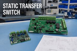
blank circuit board, https://www.bestpcbs.com/blog/2026/04/blank-circuit-board/

How to Make Circuit Board Blanks?

Circuit board blanks manufacturing involves precise, standardized multi-step processes that ensure consistency, electrical performance, and mechanical durability essential for high-reliability blank circuit board applications. Below are the key steps focusing on critical details that impact the quality of bare circuit boards:
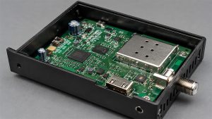
1. Material Preparation

  • Select the appropriate substrate material (FR-4, high-TG, aluminum, Rogers, or polyimide) based on the blank PCB’s intended use (e.g., Rogers for high-frequency aerospace applications, polyimide for flexible medical implants).
  • Laminate copper foil (typically 1oz-4oz) to the dielectric substrate under controlled high heat (170°C-200°C) and pressure ensuring strong adhesion between layers for multi-layer circuit board blanks.
  • Cut the laminated core material to the required panel size and prepare multilayer stacks with prepreg (insulating material) between layers to ensure electrical isolation and structural integrity.

2. Imaging Process

  • Apply a photosensitive photoresist (liquid or dry film) to both sides of the copper-clad substrate ensuring uniform coverage to protect the copper during etching.
  • Expose the photoresist-coated blank circuit board to UV light through a precision artwork film (containing the circuit pattern) hardening the photoresist in areas that will remain as conductive traces.
  • Develop the board to remove the unexposed (unhardened) photoresist revealing the copper areas that will be etched away leaving the desired circuit pattern on the blank PCB.

3. Etching Process

  • Etch the exposed copper using a chemical solution (typically ferric chloride or cupric chloride) removing unwanted copper to leave only the conductive traces, pads, and vias of the blank circuit board.
  • Strip the remaining hardened photoresist using a chemical stripper revealing the clean copper circuit pattern on the bare circuit board.
  • Clean and inspect the panels for etching defects (over-etching, under-etching, trace damage) using AOI or manual inspection ensuring the circuit pattern matches design specifications.

4. Drilling & Plating

  • Drill precision holes (through-hole or micro-vias for HDI boards) using CNC drilling equipment ensuring accurate hole size and location for component pins and interlayer connections in multi-layer blank PCBs.
  • Desmear the hole walls to remove resin residue from drilling then clean the holes to ensure proper copper adhesion for plating.
  • Apply electroless copper plating (thin, uniform copper layer) to the hole walls and board surface followed by electrolytic copper plating to achieve the desired copper thickness (1oz-4oz) for the blank circuit board.
  • Perform pattern plating (if needed) to thicken copper on critical traces (e.g., power traces) for enhanced current-carrying capacity ensuring the circuit board blanks meet electrical requirements.

5. Final Processing

  • Apply a solder mask (typically green but available in other colors) to the blank circuit board covering all areas except pads and vias to protect traces from oxidation, short circuits, and physical damage.
  • Add legend/identification printing (silk screen) to the solder mask marking component designators, logos, and polarity indicators for easy assembly and troubleshooting.
  • Apply the desired surface finish (HASL, lead-free HASL, ENIG, OSP, or immersion silver) to the pads ensuring strong solderability and corrosion resistance for the blank PCB.
  • Route or punch the panels to the final blank circuit board dimensions removing excess material and ensuring clean, precise edges.
  • Conduct final electrical testing (continuity, isolation, impedance) and visual inspection rejecting any bare circuit boards with defects to ensure only high-quality products are delivered.

Where to Buy Blank Circuit Boards?

For high-quality blank circuit boards, partner with specialized manufacturers like EBest. Key considerations when selecting a supplier:

Critical Selection Criteria

  • Technical Capabilities: Layer count, minimum trace/space, hole size
  • Quality Systems: Certifications (ISO 9001, IATF 16949, ISO 13485)
  • Material Selection: Range of substrates and surface finishes
  • Lead Times: Prototypes and mass production capabilities
  • Quality Control: Testing procedures and defect rates
  • Technical Support: DFM analysis and engineering assistance

EBest’s Advantages

  • One-Stop Solution: Design, prototype, and full production
  • Quick Quotes: 24-hour response for most inquiries
  • Flexible Order Quantities: From 1 to 100,000+ pieces
  • Global Shipping: Reliable worldwide delivery
  • Competitive Pricing: Volume discounts and cost-effective manufacturing
Blank Circuit Board, https://www.bestpcbs.com/blog/2026/04/blank-circuit-board/

How Much Does Blank Circuit Boards Cost?

Blank circuit board pricing varies based on multiple factors:

  • Board Size: Larger dimensions increase material usage
  • Layer Count: 1-layer ($2-$5) to 20-layer ($50-$200+)
  • Complexity: Trace/space, hole size, aspect ratio
  • Quantity: Prototypes ($5-$50/unit) vs. mass production ($0.50-$20/unit)
  • Material: Standard FR-4 vs. high-frequency or flexible substrates
  • Surface Finish: HASL (lowest), ENIG, immersion silver, gold plating
  • Special Requirements: Impedance control, heavy copper, testing

Below is a price chart for blank circuit boards:

TypePrototype (1-10 pcs)Mass Production (1,000+ pcs)
1-layer FR-4$2-$8$0.50-$3
2-layer FR-4$5-$15$1-$5
4-layer FR-4$15-$40$3-$10
6-layer FR-4$30-$70$5-$15
8-layer High-TG$50-$120$8-$20
Flexible (Polyimide)$20-$80$5-$25
Metal Core (Aluminum)$30-$100$10-$30

FAQs About Blank Printed Circuit Board

Q1: What’s the minimum order quantity for blank PCB?

A1: EBest accepts orders from 1 piece (prototypes) to mass production. No minimum order restrictions for standard blank circuit board specifications.

Q2: How long does blank circuit board production take?

A2: Standard prototypes: 3-5 days. Mass production: 7-10 days. Express service available (24-48 hours) for urgent requirements.

Q3: What surface finishes are available for blank PCB?

A3: Common options: HASL, lead-free HASL, ENIG (Electroless Nickel Immersion Gold), immersion silver, immersion tin, and OSP (Organic Solderability Preservative).

Q4: Can blank circuit boards withstand high temperatures?

A4: Standard FR-4 handles up to 130°C continuously. High-TG materials work up to 170°C+. Metal core and ceramic substrates handle even higher temperatures for specialized applications.

Q5: What testing is performed on blank circuit boards?

A5: Standard tests include: flying probe or fixture electrical test, AOI (Automated Optical Inspection), solder mask adhesion, and dimension verification. Special testing available upon request.

Q6: Can you manufacture custom-sized blank circuit boards?

A6: Yes, EBest produces fully customized blank circuit board dimensions, shapes, and specifications according to your design files.

Ready to Order Your Blank Circuit Boards?

EBest delivers high-quality blank circuit board solutions for medical, aerospace, industrial, and commercial applications. As a leading China blank printed circuit board manufacturer, we provide comprehensive services from design through mass production.

Our blank PCB products meet the strictest quality standards with fast delivery and competitive pricing. Whether you need prototypes or large-scale production, we offer tailored solutions to meet your exact requirements.

Contact us today to discuss your blank circuit board needs. Send your specifications and requirements to sales@bestpcbs.com for a free quote and DFM analysis. Partner with EBest for reliable circuit board blanks that power your success.

You may also like