Are you struggling with dense multilayer routing, limited board space, or unstable high-speed signals in PCB layouts caused by traditional through-hole structures? Blind via PCB offer the solution, and this guide breaks down all the practical design, fabrication, and cost-saving tips you need to implement them successfully.
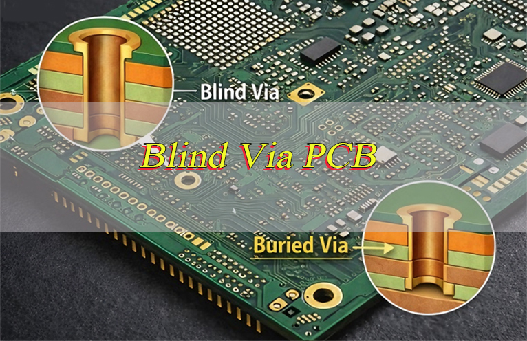
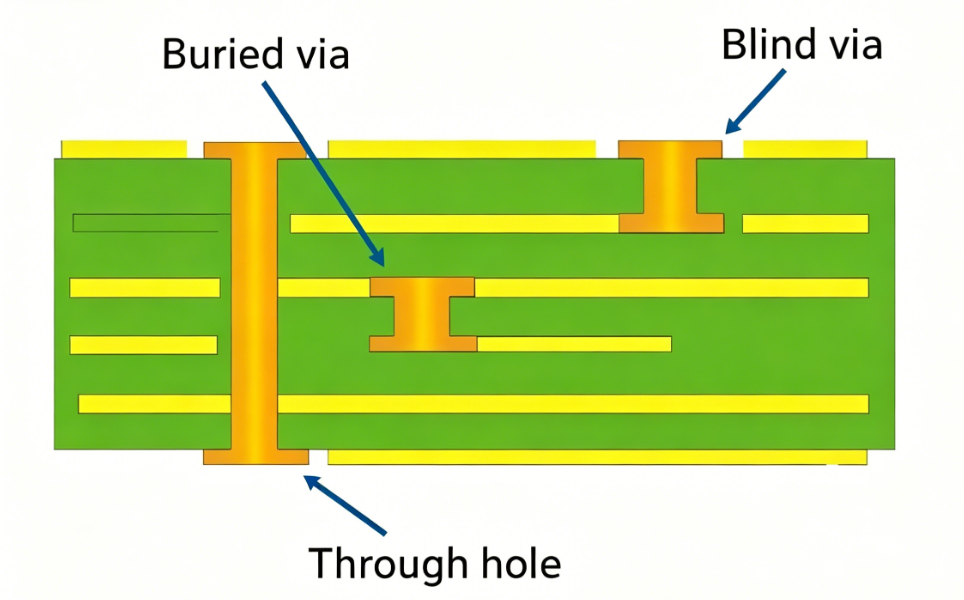
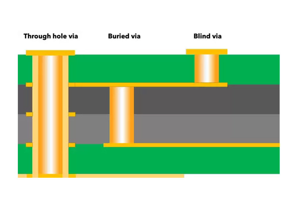
What Is a Blind Via PCB?
A blind via PCB is a type of multilayer printed circuit board that uses blind vias to connect outer layers to one or more inner layers without drilling through the entire board. Unlike traditional through-hole PCBs, blind vias do not penetrate the full board and are a core component of high-density interconnect (HDI) designs.
“Blind” means these vias are only visible from one side of the PCB and hidden from the other. They are precisely drilled to stop at a specific inner layer for targeted connections.
Blind vias solve issues in complex PCB layouts including limited space, poor signal integrity and mechanical instability. They enable compact component placement, shorter signal paths and a more balanced board structure for miniaturized, high-performance devices.
What are Differences Between Blind Via PCB and Through-Hole PCB?
Below is a comparison chart between blind via PCB and through-hole PCB:
| Comparison Items | Blind Via PCB | Through-Hole PCB |
| Board Space Utilization | High space efficiency, no full penetration, saves surface area for more components and traces; ideal for miniaturized devices. | Low space efficiency, holes penetrate the entire board, waste surface space and limit component density. |
| Signal Integrity (High-Frequency) | Excellent; shorter via paths reduce parasitic capacitance/inductance, minimize signal loss and crosstalk (suitable for ≥1 GHz designs). | Poor; longer through paths cause more signal degradation, unsuitable for high-frequency applications. |
| Manufacturing Cost | Higher; requires laser-controlled depth drilling and sequential lamination, suitable for high-performance projects. | Lower; uses simple mechanical drilling, cost-effective for basic, low-density designs. |
| Mechanical Stability & Reliability | Higher; balanced material stress reduces board warping after lamination, more reliable in harsh environments. | Lower; full penetration holes cause uneven stress, higher risk of warping and structural damage. |
| Application Suitability | Suitable for compact, high-performance devices (smartphones, medical equipment, industrial controls). | Suitable for basic, low-density devices (simple electronics, prototype boards, low-frequency equipment). |
| Fabrication Complexity | More complex; requires precise laser drilling and strict layer alignment, needs professional manufacturers. | Less complex; simple mechanical drilling, easier to fabricate, more widely available manufacturers. |
What Rules Should Be Followed for Blind Via PCB Design?
Following consistent layout standards keeps blind via PCB designs production-ready and electrically stable, reducing rework costs and production delays. Below are the non-negotiable rules for reliable designs:
- Controlled Via Sizing: Use standard drilled diameters ranging from 3 mil to 6 mil (4 mil is the industry sweet spot for balance of density and manufacturability). Keep the depth-to-diameter proportion at 1:1 or lower. Exceeding this ratio leads to poor plating coverage and voids inside the via.
- Balanced Layer Symmetry: Arrange layer structures in mirrored symmetry (top and bottom halves matching in material thickness and copper weight) to distribute thermal and mechanical stress evenly during lamination. Asymmetrical stacks almost always cause board warping.
- Fixed Clearance Requirements: Maintain a minimum 3.5 mil clearance between blind vias, regular traces, and surrounding pads (3 mil is the absolute minimum for high-volume production). This prevents short circuits and signal interference between different electrical networks.
- Proper Pad Sizing: Set pad dimensions to roughly 2–3 times the via opening size to preserve a complete annular ring (the copper ring around the via). A insufficient annular ring increases the risk of pad lifting and electrical failure.
- Avoid Via Placement Under SMT Pads: Never place blind via openings directly underneath surface mount component pads. This causes solder migration (wicking) into the via, weakening solder joints and leading to component failure.
- Adjacent Layer Connections Only: Arrange blind via connections only between adjacent layers; skipping remote internal layers complicates fabrication and increases the risk of misalignment.
- High-Tg Material Selection: Choose substrates with a glass transition temperature (Tg) of 170°C or higher to withstand repeated heating cycles during multilayer lamination. Lower Tg materials may soften or deform, ruining via integrity.
- IPC Standard Compliance: Follow IPC-2221 (design) and IPC-6012 (performance) benchmarks to match mainstream fabrication factory capabilities. Non-compliant designs often require custom tooling, increasing costs and lead times.
What Are the Specifications of Blind Vias in PCB Design?
Below are universally adopted blind via parameters for standard multilayer PCB projects, aligned with common fabrication limits and optimized for reliability. These specs balance density, manufacturability, and performance:
| Parameter | Standard Value | Minimum Value |
| Via Diameter | 4–6 mil | 3 mil |
| Pad Diameter | 8–12 mil | 6 mil |
| Aspect Ratio | 1:1 | 1.2:1 |
| Dielectric Thickness | 4–20 mil | 2 mil |
| Copper Thickness | 0.5–2 oz | 0.5 oz |
| Clearance (Via to Via) | 4 mil | 3 mil |
| Clearance (Via to Trace) | 4 mil | 3 mil |
| Solder Mask Opening | ≥2 mil larger than pad | ≥1 mil larger |
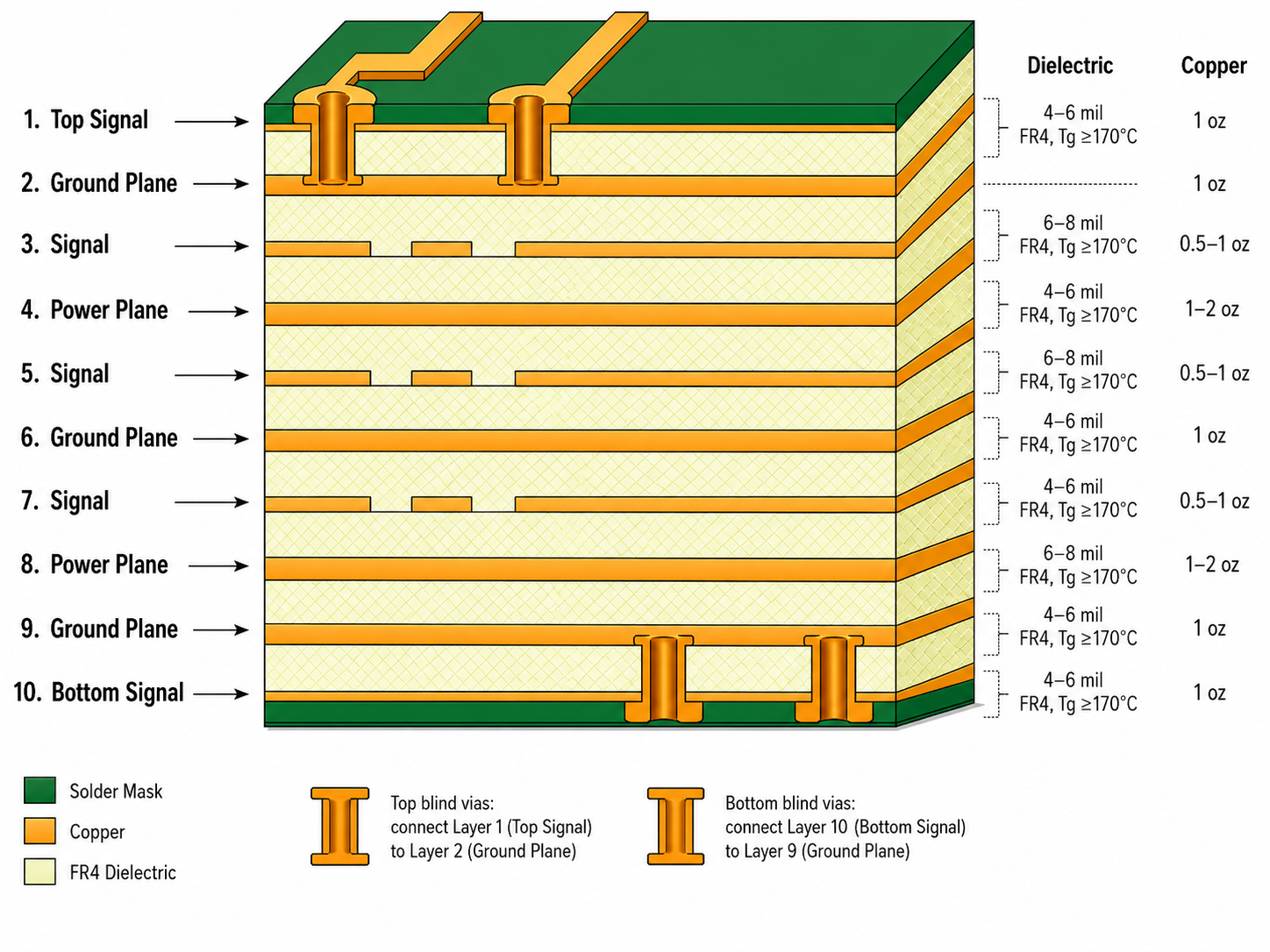
10-Layer Blind Via PCB Stackup
A widely adopted, production-friendly 10-layer blind via PCB stackup is optimized for high density, signal integrity, and manufacturability. This configuration leverages symmetric layer arrangement and standard materials to balance performance and cost, making it suitable for most high-performance 10-layer applications. The standard 10-layer stackup structure (from top to bottom, including dielectric thickness and copper weight) is as follows:
- Layer 1 (Top Signal): 1 oz copper, with blind vias connecting to Layer 2
- Dielectric (Layer 1–Layer 2): 4–6 mil (FR4, Tg ≥170°C)
- Layer 2 (Ground Plane): 1 oz copper (continuous reference plane for Layer 1 signals)
- Dielectric (Layer 2–Layer 3): 6–8 mil (FR4, Tg ≥170°C)
- Layer 3 (Signal): 0.5–1 oz copper
- Dielectric (Layer 3–Layer 4): 4–6 mil (FR4, Tg ≥170°C)
- Layer 4 (Power Plane): 1–2 oz copper (for high current distribution)
- Dielectric (Layer 4–Layer 5): 6–8 mil (FR4, Tg ≥170°C)
- Layer 5 (Signal): 0.5–1 oz copper
- Dielectric (Layer 5–Layer 6): 4–6 mil (FR4, Tg ≥170°C)
- Layer 6 (Ground Plane): 1 oz copper (central reference plane for inner signals)
- Dielectric (Layer 6–Layer 7): 4–6 mil (FR4, Tg ≥170°C)
- Layer 7 (Signal): 0.5–1 oz copper
- Dielectric (Layer 7–Layer 8): 6–8 mil (FR4, Tg ≥170°C)
- Layer 8 (Power Plane): 1–2 oz copper (for high current distribution)
- Dielectric (Layer 8–Layer 9): 4–6 mil (FR4, Tg ≥170°C)
- Layer 9 (Ground Plane): 1 oz copper (continuous reference plane for Layer 10 signals)
- Dielectric (Layer 9–Layer 10): 4–6 mil (FR4, Tg ≥170°C)
- Layer 10 (Bottom Signal): 1 oz copper, with blind vias connecting to Layer 9
How to Design 2 Sets of Blind Vias in PCB?
Two separate blind via groups (e.g., Top→Layer 2 and Bottom→Layer N-1) often appear in medium-density multilayer layouts. Proper step-by-step planning avoids layout conflicts and production defects, ensuring reliable performance:
1. Clarify Connection Requirements: Document exact layer pairs each via group needs to connect (e.g., Set 1: Top→Layer 2; Set 2: Bottom→Layer 3 in a 4-layer PCB). This prevents confusion during routing and fabrication.
2. Maintain Stackup Symmetry: Keep the overall layer arrangement symmetrical to balance stress from dual via group processing. Asymmetry can cause uneven plating and board warping.
3. Reserve Dedicated Zones: Allocate separate layout zones for each via set and maintain a minimum 4 mil clearance between groups. This avoids signal interference and simplifies drilling.
4. Standardize Via Sizing: Apply identical via (4–6 mil) and pad (8–12 mil) sizing standards to both groups for a unified production flow. Mixed sizes increase manufacturing complexity and cost.
5. Optimize Trace Routing: Route signal traces to match the nearest via group to keep trace lengths concise. Shorter traces improve signal integrity and reduce crosstalk.
6. Run DFM Checks: Use design-for-manufacturing (DFM) tools to confirm spacing, alignment, and drilling limits. Most manufacturers provide free DFM checks to catch issues early.
7. Simulate Signal Integrity: Complete basic signal simulation (using tools like Altium or Cadence) to rule out noise caused by improperly placed blind vias. This is critical for high-speed designs.
How to Design 4 Sets of Blind Vias in PCB?
Four independent blind via groups (e.g., Top→Layer 2, Top→Layer 3, Bottom→Layer N-1, Bottom→Layer N-2) are common in high-density 8+ layer designs (e.g., medical devices, aerospace components). Follow these steps to arrange structures without fabrication issues:
1. Map All Connections: Document every layer connection point for all four via groups across the full stackup. For example, in a 10-layer PCB: Set 1 (Top→Layer 2), Set 2 (Top→Layer 3), Set 3 (Bottom→Layer 8), Set 4 (Bottom→Layer 9).
2. Optimize Stackup for Density: Use thinner standard dielectric materials (4–6 mil) between layers with dense blind via placement. Thinner dielectrics reduce via depth, keeping the aspect ratio at 1:1.
3. Enforce Clearance Rules: Maintain aminimum 4 mil clearance between all separate via groups and avoid overlapping projections. This prevents short circuits and eases drilling alignment.
4. Use Staggered Placement: Position via openings in staggered patterns (not aligned vertically) to reduce concentrated mechanical stress. This improves board durability, especially in flexible or high-vibration applications.
5. Strengthen Inner Layers: Increase copper thickness (to 1–2 oz) on inner layers carrying multiple blind via current paths. This improves current-carrying capacity and reduces thermal buildup.
6. Coordinate with Sequential Lamination: Work with your manufacturer to align the design with sequential lamination steps (sub-assemblies) to accommodate four blind via sets. Sequential lamination ensures precise layer alignment.
7. Complete Full DFM Verification: Run a comprehensive DFM check covering size, spacing, layer alignment, and plating requirements. This step is non-negotiable for high-density designs to avoid rework.
What Are Common Blind Via PCB Design Problems and Solutions?
Layout teams regularly encounter repeatable blind via-related issues during project development. Below are the most common problems, along with practical fixes that apply directly to most multilayer PCB tasks:
Excessive Aspect Ratio: Aspect ratio >1:1 creates incomplete hole plating and internal gaps, leading to electrical failure.
Solution: Reduce dielectric thickness between connected layers or expand via diameter to bring the ratio back to 1:1. For example, a 4 mil via can safely span a 4 mil dielectric (1:1 ratio).
Insufficient Annular Ring: Small pad sizing or layer misalignment leaves insufficient copper around via edges, increasing pad lifting risk.
Solution: Expand pad dimensions to 2–3× the via diameter and ensure layer alignment tolerance ≤2 mil during file setup.
Via Overlap with SMT Pads: Blind vias under surface mount pads cause solder absorption into hole openings, weakening joints.
Solution: Relocate via positions outside pad boundaries or adopt solder mask-defined (SMD) pads for micro vias in pad (VIP) designs.
Signal Integrity Degradation: Uncontrolled via placement introduces extra capacitance and inductance, affecting high-speed signals.
Solution: Reduce unnecessary via usage, shorten signal paths, and place grounded shielding vias (stitch vias) beside sensitive signal lines to minimize noise.
Production Cost Overruns: Overly complex blind via arrangements push costs higher than necessary.
Solution: Stick to standard via sizes (4–6 mil), limit via group quantity to only essential connections, and reuse proven stackup layouts across projects.
Layer Misalignment: Minor layer shifting during lamination creates open circuits at blind via connections.
Solution: Add fiducial alignment marks to the PCB (for precise laser drilling) and verify layer alignment tolerance with your manufacturer before production.
What Stages Are in the PCB Blind Via Fabrication Process?
Production flow for boards with blind via structures follows a precise, ordered sequence different from regular PCB manufacturing. Each step is critical to ensuring via integrity and overall board quality:
1. Layer Preparation: Cut raw copper-clad substrates to required panel size and clean surface contaminants (oil, dust) thoroughly. Clean surfaces ensure strong adhesion between layers during lamination.
2. Inner Layer Patterning: Apply photoresist to inner layers, expose the circuit pattern using a photomask, develop the resist, and etch away excess copper. Strip the remaining photoresist to reveal the final inner circuit.
3. First Lamination: Combine prepared inner core layers with dielectric prepreg material under controlled heat (170–180°C) and pressure. This bonds the layers into a single core stack, forming the foundation of the blind via PCB.
4. Blind Via Drilling: Use laser equipment to drill blind openings with precise depth control from outer surfaces inward. Laser drilling ensures accuracy for small via sizes (3–6 mil) and consistent depth stopping at the target inner layer.
5. Desmear and Plating: Remove residual drilling debris (smear) from via walls using chemical or plasma cleaning. Apply electroless copper plating to line the via walls, then electroplate to the required thickness (0.5–2 oz) for electrical conductivity.
6. Outer Layer Patterning: Apply photoresist to outer layers, expose/develop the circuit pattern, and etch excess copper. This step creates the outer circuit traces and pads.
7. Solder Mask Application: Apply liquid solder mask to the board, cure it under UV light, and expose/develop openings for component pads and vias. Solder mask protects copper from oxidation and prevents short circuits.
8. Surface Finish: Apply a surface finish (ENIG, HASL, OSP) to protect exposed copper and enhance solderability. ENIG is preferred for blind via PCB designs due to its flat surface and compatibility with fine-pitch components.
9. Testing and Inspection: Perform electrical tests (continuity/insulation) to verify circuit integrity, automated optical inspection (AOI) to detect surface defects, and cross-section sampling to confirm via plating quality (no voids or uneven coverage).
What Affects Blind Via PCB Cost and How to Optimize It?
Production cost for boards with blind via structures is higher than standard PCBs due to complex processes like laser drilling and sequential lamination. Understanding cost factors and simple optimization strategies helps reduce expenses without sacrificing performance:
- Number of Blind Via Sets: Additional blind via groups add more drilling, plating, and lamination steps. Optimization: Limit group quantity to only the connections the layout truly requires. Combine signals where possible to reduce via count.
- Via Size and Density: Extremely small, densely packed vias demand slower laser processing time. Optimization: Use industry-standard 4–6 mil diameter vias and avoid overcrowding layout zones. Denser vias increase drilling time and defect rates.
- Stackup Complexity: Non-symmetric or non-standard thickness stacks require custom tooling. Optimization: Use symmetric stacks with standard dielectric thicknesses (4, 6, 8 mil) to leverage existing factory tooling and reduce costs.
- Material Selection: High-Tg or high-frequency materials (e.g., Rogers) cost more than standard FR4. Optimization: Use FR4 (Tg 150/Tg 170) for most applications; reserve special materials only for high-frequency or high-temperature circuits.
- Manufacturing Volume: Small-batch orders carry fixed setup costs per production run. Optimization: Consolidate similar projects into unified production panels to improve material utilization and spread setup costs.
- Testing Requirements: Additional tests (cross-section, X-ray) add cost. Optimization: Limit destructive testing (cross-section) to critical designs; use AOI and electrical testing for standard inspection.
What to Consider When Selecting a Blind and Buried Vias PCB Manufacturer?
Selecting a suitable fabrication partner ensures stable production quality for layouts with blind via features. Below are the key factors to evaluate before choosing a manufacturer:
- HDI Manufacturing Experience: Confirm hands-on experience building multilayer boards with blind/buried vias and sequential lamination. Ask for case studies or samples of similar projects to verify expertise.
- Laser Drilling Capability: Verify laser drill precision (minimum 3 mil diameter) and depth control. Manufacturers with advanced laser equipment (e.g., UV laser) produce more consistent blind vias.
- Layer Alignment Precision: Check layer registration tolerance (≤2 mil) to prevent misalignment. This is critical for dense blind via layouts. Poor alignment leads to open circuits and rework.
- Plating Quality: Ensure capability for uniform copper plating in blind vias (no voids or uneven thickness). Ask for cross-section reports to verify plating integrity.
- Material Range: Confirm availability of required materials (high-Tg, high-frequency, aluminum substrates) to avoid supply delays.
- Testing Facilities: Verify in-house AOI, electrical test, and cross-section analysis capabilities. In-house testing reduces lead times and ensures quality control.
- Quality Certifications: Look for ISO 9001, IPC-6012 compliance, and Class 3 certification if your project requires high reliability (e.g., medical, aerospace).
- Cost and Lead Time: Compare quotes while ensuring quality; confirm lead times for prototype and volume orders. Avoid manufacturers with unrealistically low prices. They often cut corners on plating or alignment.
How to Find Reliable PCB Fabricators with Blind and Buried Vias?
Sourcing dependable PCB suppliers for blind via projects follows a structured, practical approach to avoid costly mistakes. Use these steps to identify reliable partners:
- Review Technical Capabilities: Check the manufacturer’s website for blind via specifications (minimum size, aspect ratio, layer count). Ensure their capabilities match your design requirements (e.g., 3 mil vias, 10-layer stacks).
- Request Samples and References: Ask for customer references with similar blind via projects; contact references to feedback on quality, lead times, and communication. Request physical samples to inspect via quality and board finish.
- Evaluate Prototyping Services: Test manufacturer quality with a small prototype order before volume production. Prototypes reveal potential issues (e.g., misalignment, poor plating) early, avoiding costly volume rework.
- Assess DFM Support: Choose manufacturers that provide detailed DFM feedback to optimize your design for production. Good DFM support catches issues before fabrication, reducing costs and delays.
- Compare Quotes: Obtain quotes from 3–5 qualified manufacturers; balance cost with quality and capability. The lowest quote is not always the best. Prioritize reliability and process capability.
- Check Online Reviews: Look for reviews on industry forums and social media; avoid manufacturers with consistent quality complaints (e.g., layer misalignment, delayed orders).
FAQs About Blind Via PCB
Q1: What are the differences between blind and buried vias in PCB design?
A1: Blind vias connect outer layers to inner layers (visible on one surface), while buried vias connect only inner layers (not visible on any surface). Blind vias are simpler and cheaper to manufacture than buried vias, which require additional sequential lamination steps. Blind vias are ideal for medium-density designs, while buried vias are used for high-density layouts where surface space is extremely limited.
Q2: What are the minimum dimensions for blind vias in aluminum PCB?
A2: Aluminum PCBs with blind vias typically have a minimum via diameter of 4 mil and an aspect ratio ≤1:1. The thermal conductivity of aluminum requires careful thermal management during manufacturing. Laser drilling must be controlled to avoid overheating the substrate, which can cause warping or delamination. Additionally, copper plating thickness should be at least 1 oz to ensure good thermal and electrical conductivity.
Q3: Can blind vias be used in FR4 PCB for high-frequency applications?
A3: Yes. FR4 PCB with blind vias is suitable for high-frequency designs up to 10 GHz. Shorter blind via paths reduce signal loss and improve integrity compared to through holes, which have longer paths and higher parasitic capacitance. For frequencies above 10 GHz, consider high-frequency materials (e.g., Rogers) paired with blind vias to further minimize signal degradation.
Q4: What are the design considerations for blind vias in rigid-flex PCB?
A4: Blind via placement on rigid-flex PCB must stay clear of all flexible circuit regions. Vias in flex zones will crack or break during bending. Use larger vias (≥6 mil) in rigid areas to improve reliability, and maintain a minimum 4 mil clearance from flex boundaries. Additionally, use flexible dielectrics (e.g., polyimide) between layers with blind vias to ensure the board retains its flexibility.
Q5: How to design blind vias for sinkpad PCB in power applications?
A5: Sinkpad PCB blind vias should be arranged in arrays under power components to maximize thermal transfer. Use 6–8 mil diameter vias with 0.5–1 oz copper plating, and connect the vias to a ground plane to efficiently dissipate heat. Space vias evenly (4–6 mil apart) to ensure uniform heat distribution, and avoid placing vias too close to component edges to prevent solder joint issues.