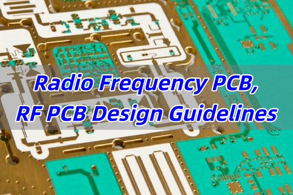
Have you ever wondered why engineers talk about high frequency PCB and high speed PCBs as if they’re completely different technologies—even though they both deal with signals in the GHz range? It’s a common point of confusion, and the truth is that these two types of circuit boards serve very different purposes, even if they sometimes overlap in the same system.
Whether you’re designing RF modules, 5G antennas, or high-speed digital hardware, this article gives you the clarity you need to make the right technical decisions.
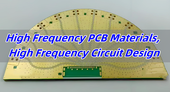
What Is a High Frequency PCB?
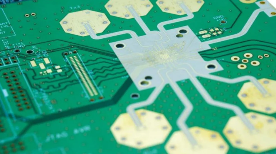
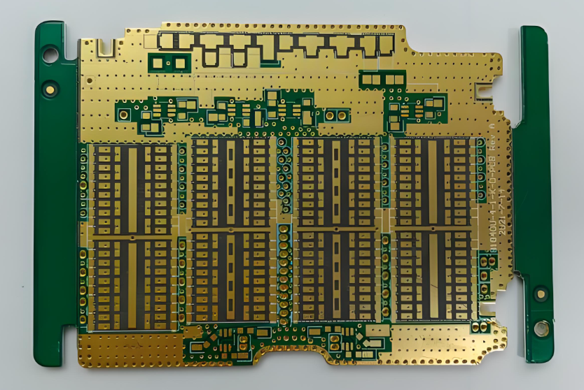
A high frequency PCB is a printed circuit board designed to operate at frequencies above 500 MHz, and in RF/microwave applications typically from 1 GHz to 77 GHz (and beyond). These circuits carry analog RF signals where signal integrity depends heavily on dielectric behavior, phase stability, and transmission line accuracy.
Because electromagnetic waves at these frequencies are extremely sensitive to loss, materials and PCB structures must remain consistent across the entire board.
Key characteristics of high frequency PCBs include:
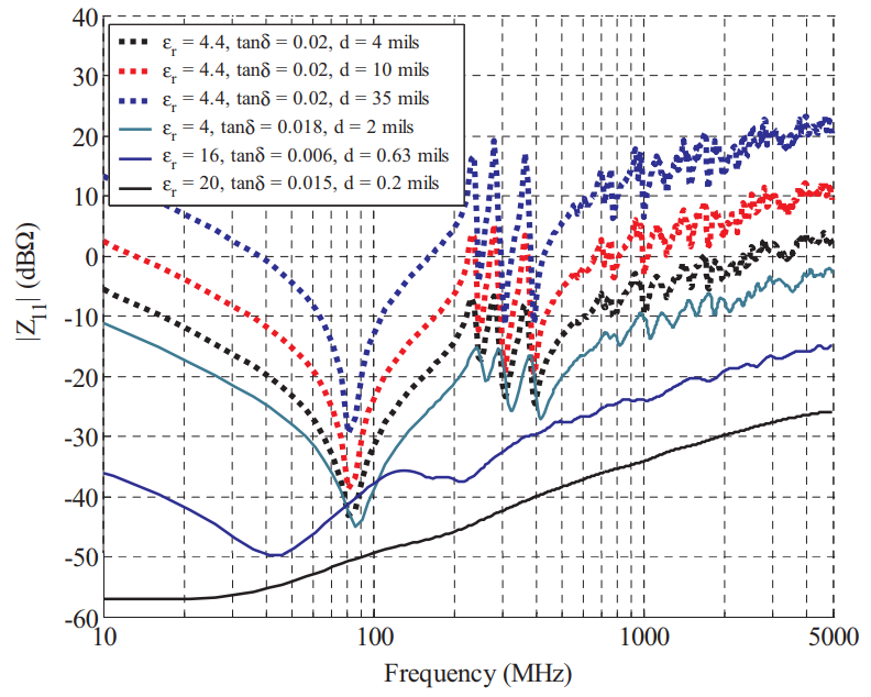
- Very low dielectric loss (Df ≤ 0.005 in many RF materials)
- Stable dielectric constant (Dk tolerance within ±0.03)
- High dimensional and thermal stability
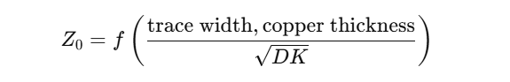
- Precise impedance-controlled transmission lines
- Use of specialized laminates like Rogers, Taconic, or PTFE-based materials
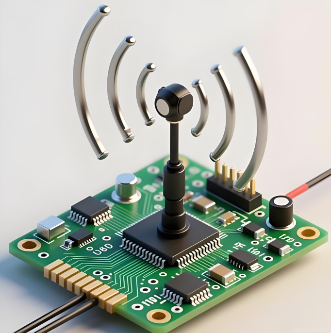
High frequency PCBs are essential in RF, 5G millimeter wave, radar, satellite systems, and microwave communications.

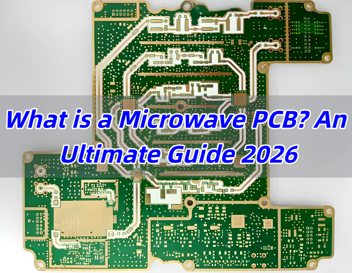
What Is a High Speed PCB?
A high speed PCB focuses on the integrity of digital signals with fast rise/fall times (not necessarily high analog frequency). In high-speed digital design, the primary goal is to ensure that the signal transitions propagate without distortion, crosstalk, jitter, or timing failures.
High speed PCBs usually operate in the hundreds of MHz to several GHz, but the defining parameter is edge rate, not the signal frequency.
Key characteristics of high-speed PCBs:
- Strong emphasis on impedance control for DDR, USB, PCIe, HDMI, and SerDes
- Controlled routing for skew, timing, return path, and crosstalk
- Use of PCB materials with low loss (Df 0.008–0.02) for digital integrity
- Multilayer stackups optimized for reference planes, differential pairs, and power integrity
High-speed PCBs are used in servers, automotive ADAS, AI hardware, IoT devices, consumer electronics, and cloud networking systems.
High Frequency PCB vs High Speed PCB: What Are the Key Differences?
Both board types deal with fast signals, yet they solve different engineering problems. A high frequency PCB focuses on electromagnetic behavior in continuous-wave or modulated analog systems. A high speed PCB focuses on digital edges and their timing.
Below is a clear comparison:
| Feature | High Frequency PCB (HF / RF / Microwave) | High Speed PCB (HS / Digital) |
| Signal Type | Analog RF, microwave, millimeter-wave | Digital signals with fast edge rates |
| Operating Range | 500 MHz – 100 GHz+ | 100 MHz – several GHz |
| Main Priority | Dk stability, loss tangent, phase accuracy | Signal integrity, timing, skew, crosstalk |
| Materials | PTFE, Rogers RO3003/RO4350B, Taconic, Teflon | FR4, Megtron 6, Isola I-Speed, low-loss epoxies |
| Routing Focus | Transmission lines (microstrip/coplanar) | Differential pairs, length tuning, return paths |
| Loss Sensitivity | Extremely sensitive | Medium to high sensitivity |
| Typical Industries | Radar, 5G, RF front-end, satellite, microwave sensors | Servers, CPUs, AI accelerators, telecom hardware |
Summary:
- High frequency PCB = analog RF performance
- High speed PCB = digital signal integrity
Both require impedance control, but HF PCBs rely heavily on material performance, while HS PCBs depend on layout and timing engineering.
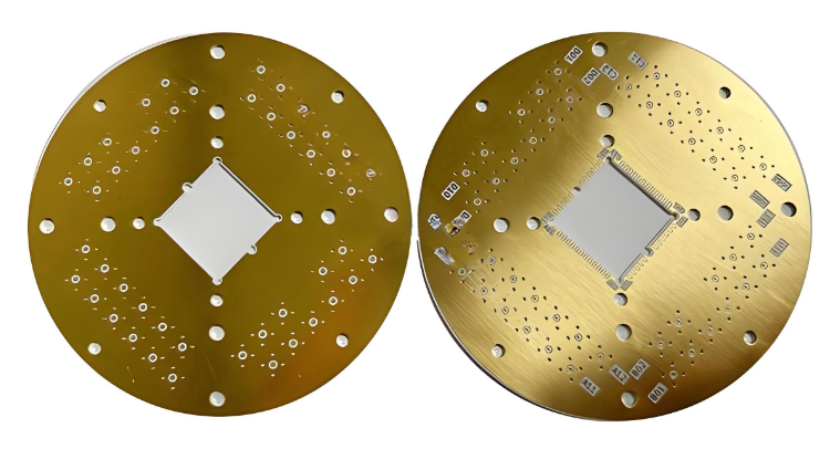
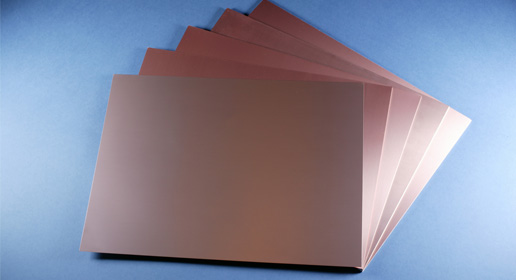
What is Best Material for High Frequency PCB Design?
Material selection is very important in a PCB manufacturing. A good laminate must hold a stable dielectric constant and maintain low loss across temperature, humidity, and frequency. These attributes reduce insertion loss and stabilize impedance.
Common high frequency PCB materials include:
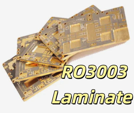
1. Rogers RO3003 laminate
A popular low-loss RF laminate.
- Dk ≈ 3.00
- Tight tolerance across the board
- Widely used for 24 GHz and 77 GHz radar, antennas, and precision RF paths
2. Rogers RO4350B laminate
A hydrocarbon ceramic material with stable electrical performance.
- Dk ≈ 3.48
- Very good loss performance for mid-GHz RF
- Easier to fabricate compared with PTFE
3. PTFE-based laminates (RO5880, Taconic, etc.)
PTFE delivers ultra-low loss and excellent Dk stability.
- Ideal for satellite work
- Strong performance in microwave and millimeter-wave designs
4. Hybrid stackups
Some designs combine PTFE layers with FR4 or hydrocarbon layers to balance cost and RF stability. This approach reduces material expense while keeping critical layers low-loss.
High frequency PCB materials must remain stable under frequency sweep. Even small Dk drift changes phase velocity and affects filter tuning, antenna gain, and RF link range. Material planning is one of the most important steps in high frequency PCB design.
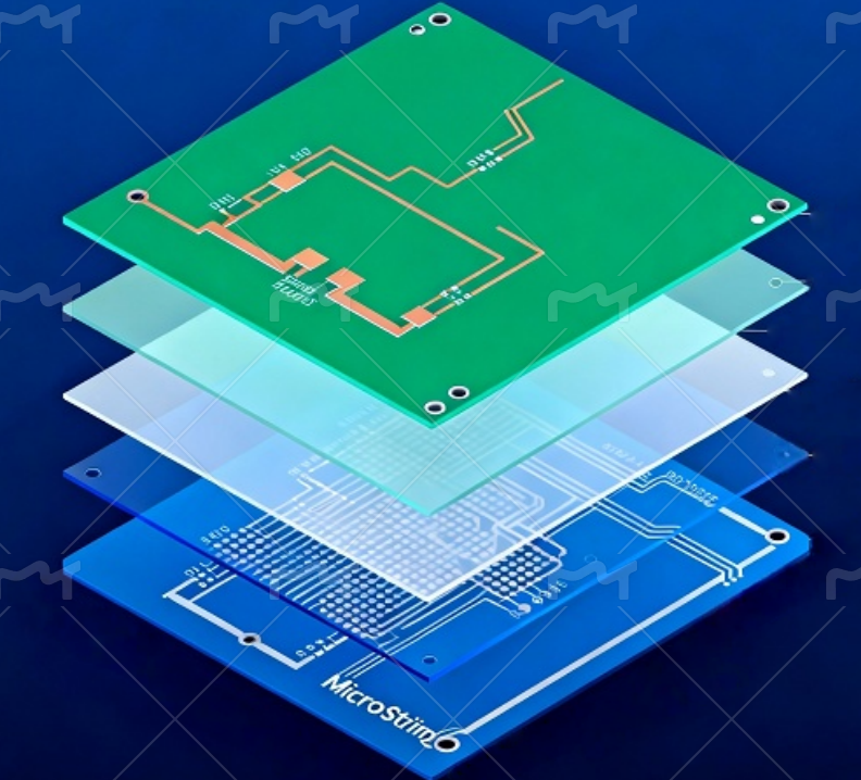
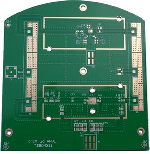
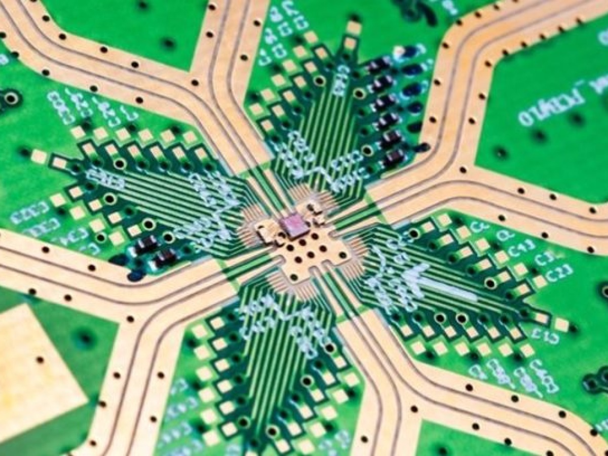
High Frequency PCB Stackup and Impedance Control
High frequency stackups require precise control over dielectric thickness, copper profile, and trace geometry.
Key stackup considerations:
- Dielectric thickness tolerance ±2–3%
- Low-profile copper (VLP / RTF) to minimize conductor loss
- Use of microstrip, stripline, and coplanar waveguides
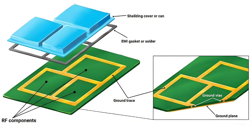
- Multiple ground layers for shielding
- Tight impedance control (±5% or better)
Common impedance targets:
- 50Ω single-ended
- 75Ω for some RF systems
- 100Ω differential for high-speed digital + RF hybrids
High Frequency PCB Routing Rules for RF, 5G, and Microwave Designs
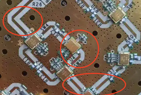
1. Use controlled-impedance transmission lines (microstrip/CPWG/stripline).
2. Maintain consistent reference planes beneath RF traces.
3. Avoid 90° bends; use 45° bends or arc routing.
4. Keep RF traces short and direct.
5. Use via stitching around RF paths for shielding.
6. Minimize via transitions (each via adds inductance).
7. Match electrical lengths precisely for filters and antennas.
8. Place RF components in a clean, isolated zone far from noisy digital circuits.
5G and millimeter wave applications require extremely tight control of conductor surface roughness, dielectric uniformity, and grounding structure.
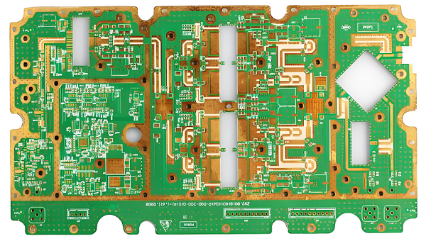
Typical High Frequency PCB Applications
High frequency PCBs are widely used in systems requiring fast electromagnetic wave propagation.
Main application fields:
- 5G base stations & mmWave antennas
- Radar systems (24 GHz, 77 GHz automotive radar)
- RF power amplifiers
- Satellite communication (Ku/K/Ka band)
- Microwave sensors
- LNBs, filters, couplers, RF transceivers
- Wireless routers, IoT RF modules, Bluetooth, Wi-Fi 6/7 devices
Wherever RF accuracy and low loss are critical, high frequency PCB materials dominate.
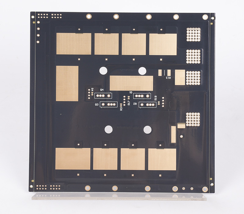
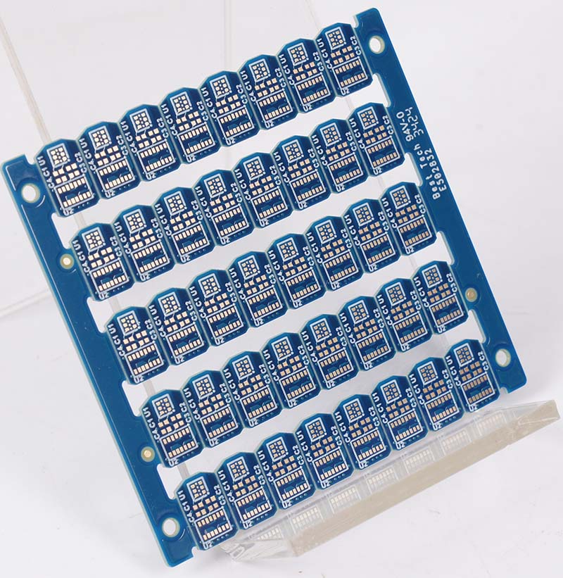
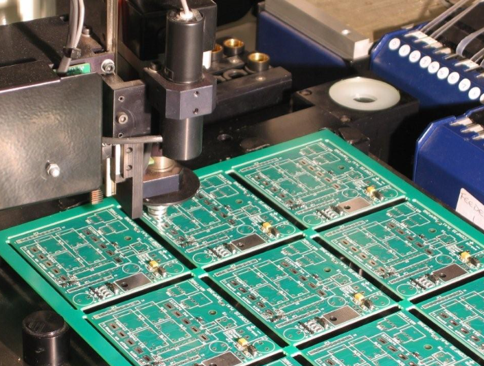
Why Choose EBest Circuit (Best Technology) as Your High Frequency PCB Supplier?
As a leading RF and microwave PCB manufacturer, EBest Circuit (Best Technology) provides stable production for demanding RF, 5G, and microwave applications. EBest Circuit (Best Technology) offers:
- Over 17 years of RF PCB manufacturing experience
- Support for Rogers, Taconic, PTFE, hydrocarbon, and hybrid stackups
- High-precision impedance control ±5% or better
- Ability to fabricate 1–40 layer HF multilayers
- Low-profile copper and high-frequency plating capability
- Advanced AOI, laser drilling, back-drill, and tight-tolerance machining
- Full engineering DFM support for RF layouts
- Proven reliability in defense, telecom, automotive radar, and aerospace projects
If you need RF or microwave PCB manufacturing with consistent performance, EBest Circuit (Best Technology) provides fast lead times, stable quality, and expert engineering support. Contact us get your PCB prototype right now!
FAQs
1. Is a high frequency PCB the same as an RF PCB?
Not exactly. RF PCBs are a subset of high frequency PCBs and usually refer to analog circuits under 6 GHz, while high frequency PCBs may go up to 100 GHz or more.
2. Can FR4 be used for high frequency PCB design?
FR4 can be used up to ~1 GHz, but losses become too large beyond that. Rogers or PTFE materials are recommended for low loss.
3. What is the typical impedance for RF PCBs?
50Ω single-ended and 100Ω differential are the most common.
4. What frequency is considered “high speed digital”?
Generally above 100 MHz clock, or any signal with rise times <1 ns.
5. Why is copper roughness important?
Rough copper increases conductor loss, especially above 10 GHz.
6. Can I combine FR4 and Rogers in the same PCB?
Yes, hybrid stackups reduce cost and are common in 5G and IoT RF modules.
7. What determines material selection for RF PCBs?
Loss tangent (Df), dielectric constant stability, thermal reliability, and manufacturing tolerance.