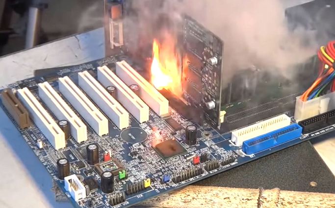
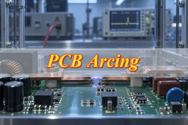
PCB arcing occurs when insulation between two conductive points breaks down and an ionized path carries current across air or along a surface. The visible flash may last only an instant, yet it can pit copper, melt solder, damage components, or carbonize the laminate. That carbonized path can lower the resistance between the same nodes and make another discharge easier to start.
The practical task is to find where the discharge traveled, what voltage actually appeared across that path, and why the insulation system could not withstand it. Those answers determine whether the correction belongs in the circuit, PCB layout, component selection, mechanical assembly, cleaning process, protective coating, or verification plan. A visibly charred board should remain de-energized until its damage and stored-energy hazards have been assessed.
What Is PCB Arcing, and What Happens When It Occurs?
PCB arcing is a high-current electrical discharge across a path that was intended to be insulating. It can jump through air between conductors, travel over a contaminated board surface, or connect a PCB node to a lead, connector shell, heatsink, screw, shield, or enclosure.
The discharge begins when the local electric field exceeds what the air, surface, or insulation system can withstand. Once a conductive plasma path forms, the current depends on the source impedance and available energy. A current-limited test source may produce a short flash; a low-impedance supply or charged capacitor can sustain the arc long enough to remove copper and damage the substrate.
Damage can continue after the first event:
- Metal erosion: The arc can pit traces, connector pins, component leads, and solder joints, changing their current capacity and geometry.
- Thermal damage: Local heat can melt solder, crack a package, delaminate the board, or ignite nearby material.
- Carbonization: Burned resin can become partially conductive, creating a lower-resistance surface path for repeat tracking or arcing.
- Circuit disturbance: A brief discharge can reset a processor, corrupt sensing, trip protection, or place an unexpected voltage on a low-voltage domain.
- Hidden insulation loss: Damage may extend below a component or into the laminate even when the board powers up again.
The burn mark is therefore evidence of a failed insulation path, not a complete root-cause diagnosis. The initiating event may have been a transient, contamination, a loose connection, a layout feature, or a component failure that no longer exists after power is removed.
What Causes PCB Arcing?
PCB arcing occurs when voltage stress, insulation weakness, and available fault energy combine at one physical path. A cause analysis should separate five families because each one requires a different correction.
- Electrical stress: Excessive working voltage, switching overshoot, inductive kickback, surge, hot-plug transients, transformer ringing, or motor regeneration can exceed the intended insulation level.
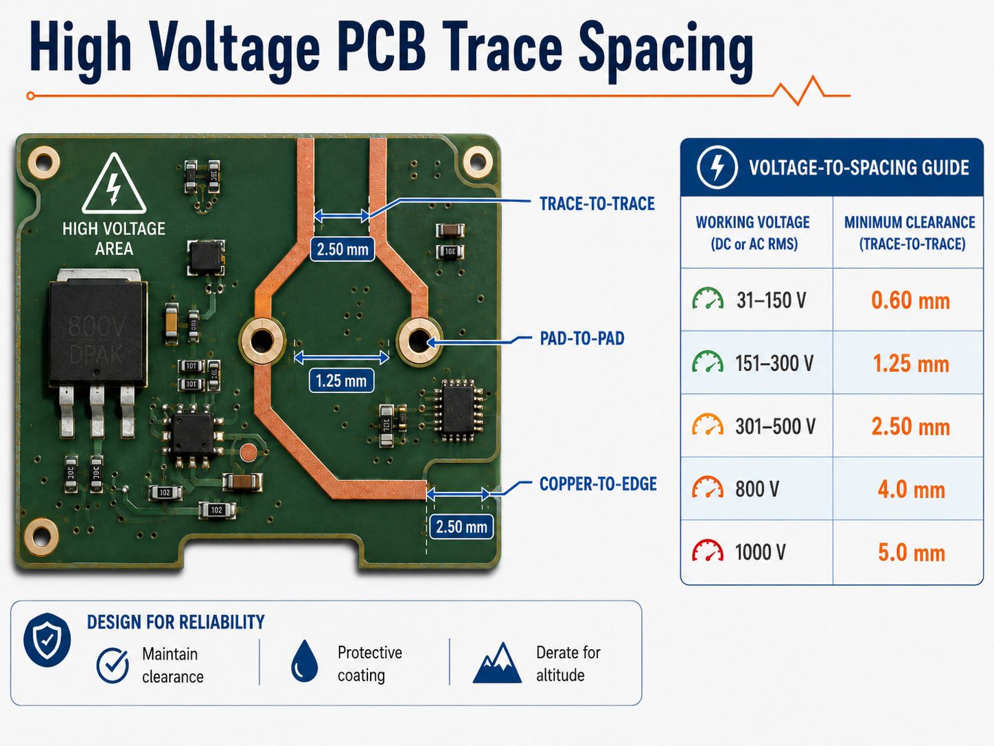
- Layout and geometry: Insufficient clearance or creepage, sharp copper tips, exposed pads, closely spaced test points, board-edge copper, and copper beneath an isolation component can concentrate the field or shorten the path.
- Environment: Condensation, conductive dust, salt, oil, and ionic residue can reduce surface resistance. Lower air density at altitude reduces air insulation strength and makes clearance more demanding.
- Materials and protection: A laminate with unsuitable tracking resistance, damaged solder mask, voided coating, cracked potting, or aged insulation may no longer provide the assumed barrier.
- Components and assembly: Wrong packages, long or bent leads, solder spikes, loose terminals, conductive hardware, contaminated connectors, and shifted components can defeat a correct nominal PCB gap.
The source also controls the outcome. The same weak path may create only leakage on a limited source but develop into destructive arcing when a capacitor bank, mains input, battery, or high-power converter supplies enough current. Root-cause work must identify both what initiated breakdown and what allowed the event to continue.
Why Can PCB Arcing Occur Even When the Nominal Voltage Seems Safe?
Nominal voltage can hide the peak differential voltage across the actual discharge nodes. PCB arcing responds to the instantaneous electric field, including transients and floating-node movement, rather than the number printed on the supply label.
A 48 V motor controller, for example, may expose a switching node to ringing or regenerative voltage well above the DC bus during braking. Opening a relay or interrupting current through an inductor can generate a short kickback pulse. Startup, shutdown, load dump, hot-plugging, and transformer leakage inductance can produce similar stress. A regulator input rated for the steady rail does not prove that every board gap sees only that rail voltage.
Measure the voltage between the two points that define the suspected arc path. Trace-to-ground measurements can miss a larger differential between two switching nodes, a node and a heatsink, or a primary-side conductor and a floating secondary assembly. Capture the relevant startup, shutdown, load, fault, and environmental states with probes and methods rated for the expected voltage and common-mode stress.
This distinction also explains why an unpowered resistance check may show no short. The initiating transient disappears when power is removed, and an air gap can read open until its breakdown voltage is exceeded. Conversely, carbonized damage may become more conductive with humidity or voltage even if a handheld meter does not reveal a hard short.
How Do Creepage and Clearance Affect PCB Arcing?
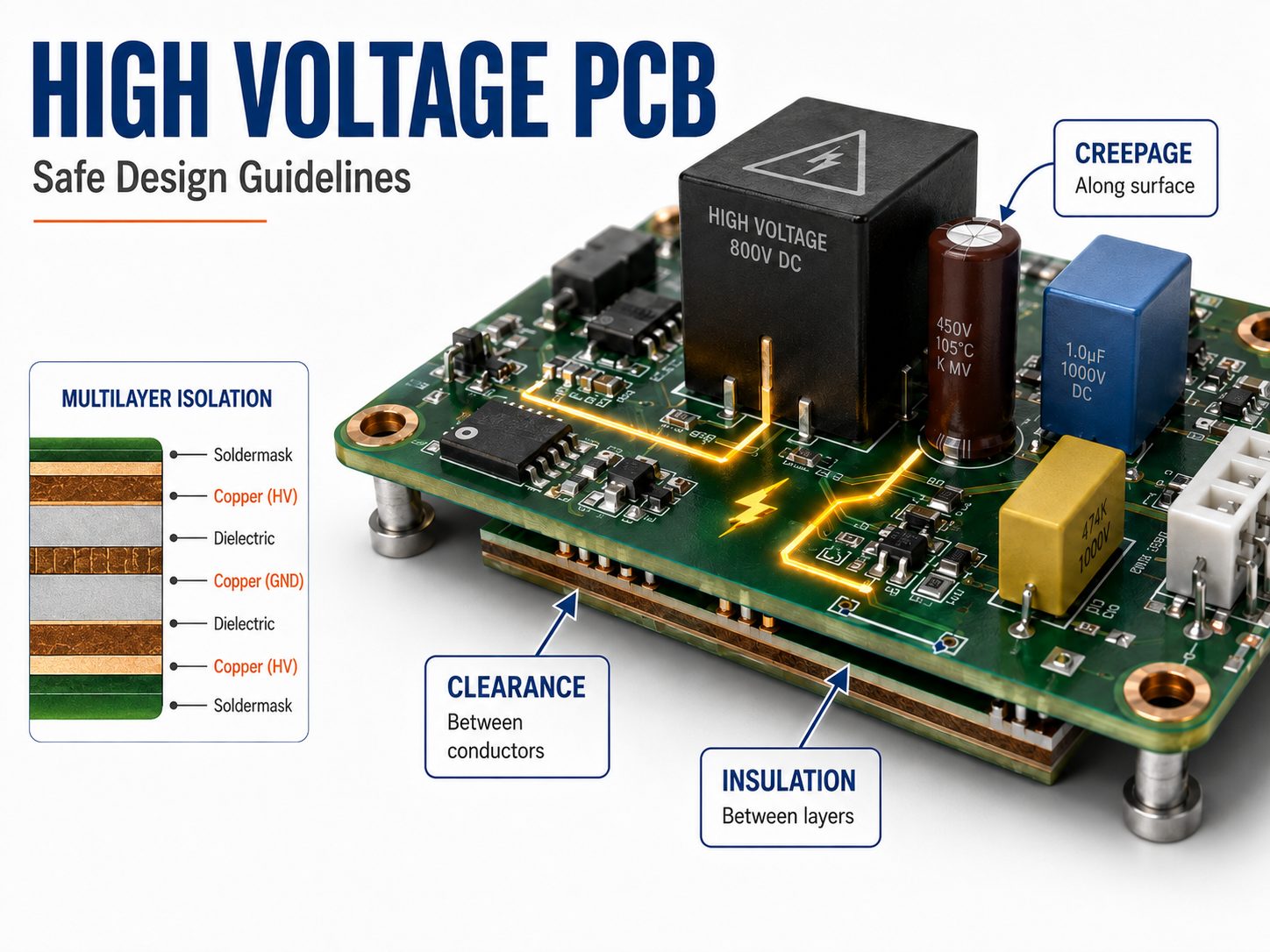
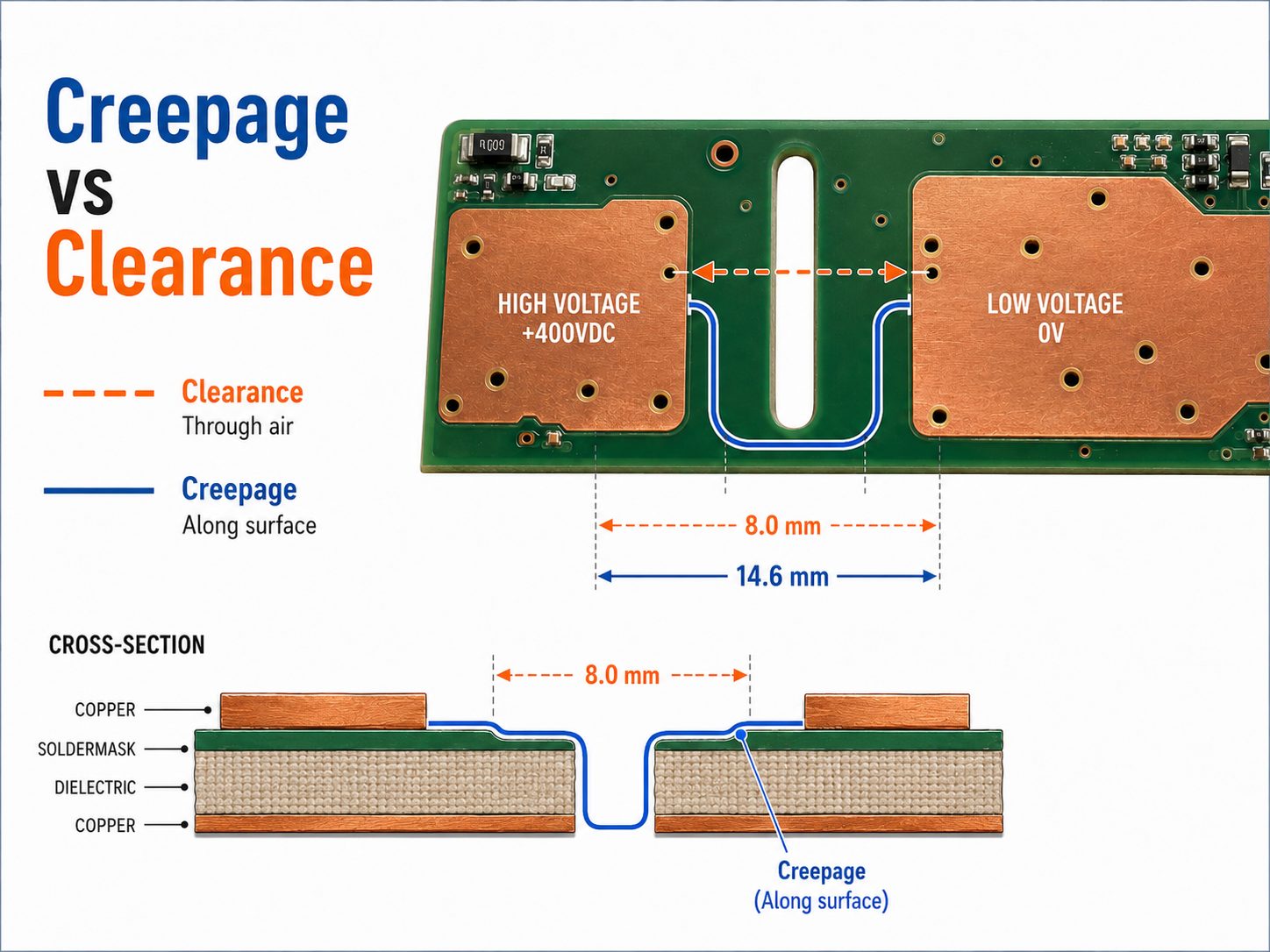
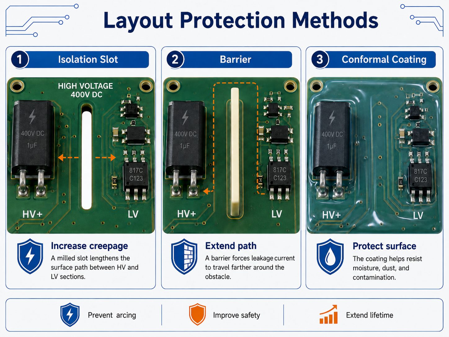
Clearance controls the shortest path through air, while creepage controls the shortest path along an insulating surface. Both must be evaluated because an assembly can have adequate copper-to-copper spacing in one view and still contain a shorter three-dimensional path.
Clearance may run from a trace to a component lead, connector shell, heatsink, shield, screw, standoff, or enclosure wall. Creepage can follow the board surface around a pad, along a slot wall, beneath a component, or across residue and coating. The copper gap shown in CAD is only one part of these paths.
The insulation function matters as much as the distance. Functional insulation keeps a circuit operating, while basic, supplementary, or reinforced insulation may protect against electric shock under specified conditions. The applicable product standard determines which insulation function is required and how working voltage, transients, pollution, materials, and altitude are applied.
For a practical review, mark voltage domains on the schematic and assembly, then inspect every boundary in three dimensions. Include tolerances, lead forming, solder fillets, component overhang, board movement, and conductive hardware. A connector or optocoupler package with inadequate pin spacing cannot be corrected by increasing only the adjacent PCB trace gap.
How Much PCB Spacing Is Needed to Prevent Arcing?
There is no universal PCB arcing distance based on voltage alone. The minimum spacing comes from the applicable end-product standard and the actual insulation conditions, not a general millimeters-per-volt rule.
The calculation or standards lookup needs these inputs:
- Voltage waveform: Identify working voltage, repetitive peak voltage, transient level, frequency, and the exact two nodes under review.
- Insulation requirement: Define functional, basic, supplementary, or reinforced insulation and whether the path is part of a safety barrier.
- Environment: Establish pollution degree, condensation risk, contamination control, and the maximum operating altitude.
- Material behavior: Use the laminate material group or comparative tracking index where the governing method requires it.
- Geometry and construction: Include the air path, surface path, slots, component packages, coating or potting system, and manufacturing tolerances.
- Applicable standard: Use the product or system standard that governs the equipment; it may modify or add to the insulation-coordination method.
A PCB spacing calculator can help organize those inputs or retrieve a table value, but its answer is only as valid as the selected standard, categories, units, and waveform. Treat a calculator result as an engineering input to review, not as proof that the entire assembled product is safe.
Which PCB Layout and Component Features Increase Arcing Risk?
The highest-risk locations combine a short physical path with high differential voltage, field concentration, contamination exposure, or assembly variation. Review actual copper and hardware instead of relying only on a global design-rule check.
- Sharp copper and exposed metal: Acute trace ends, pointed pours, narrow pad necks, test points, via rings, and solder spikes can concentrate the electric field.
- Isolation-boundary copper: Planes, thermal copper, stitching vias, and unused pads under transformers, relays, optocouplers, or connectors may shorten the intended barrier.
- Component leads and packages: Formed leads, terminal screws, relay pins, transformer windings, and power-device tabs can create paths that the bare-board spacing report does not include.
- Ground and shield features: A ground pour can reduce the distance from a high-voltage node even when it improves EMI behavior elsewhere. Connector shells and shields may be grounded, floating, or transiently driven.
- Mechanical hardware: Heatsinks, clips, mounting screws, standoffs, and enclosure walls can move within tolerance or collect contamination near a high-field node.
- Board edges and slots: Copper too close to a routed edge, incomplete slot length, plating or burrs near a cutout, and conductive debris in a slot can reduce the real path.
- Hidden assembly areas: Flux trapped beneath a component, solder balls, wire strands, metal swarf, and residue around through-hole leads can create an intermittent surface path.
Assign voltage-specific clearance rules where the EDA tool supports them, but finish with an assembly-level review. The relevant measurement is the shortest credible path after fabrication and assembly tolerances are applied.
How Do Contamination, Humidity, Altitude, and PCB Materials Affect Arcing?
Environmental conditions can turn a board that passes a clean bench test into a field failure by weakening its air or surface insulation. The mechanisms differ, so the environmental correction must match the path.
Moisture alone does not automatically create an arc. The greater surface risk appears when moisture combines with ionic flux residue, salt, dust, or another contaminant. That film can lower surface resistance, allow leakage current, create local heating, and begin tracking. Repeated discharge can carbonize the laminate until the surface becomes a much easier path.
Condensation is more severe than a stable humidity percentage because it can form a continuous conductive film. Power cycling, cold starts, outdoor enclosures, washdown, and rapid temperature changes should therefore be considered even if room-temperature operation looks acceptable.
Altitude primarily reduces the strength of air insulation, so clearance may need correction as air pressure decreases. It does not automatically increase the physical creepage path, although the product environment can still change surface contamination and moisture behavior.
Material selection affects resistance to tracking. CTI or the corresponding material group may be an input to creepage requirements, but it does not replace clearance, cleanliness, or a suitable coating process. Solder mask is a process coating with openings and tolerances; it should not be credited as safety insulation unless the applicable construction and standard explicitly permit that use.
Field failures should be compared with the real service environment: contaminant type, cleaning history, humidity and condensation cycle, altitude, temperature, airflow, enclosure sealing, and maintenance. A dry, clean prototype test cannot represent all of those conditions.
Which Design Measures Can Help Prevent PCB Arcing?
The effective correction removes the verified initiating mechanism and preserves the insulation path after manufacturing and environmental variation. Adding a coating or slot without identifying that mechanism can leave the actual hazard unchanged.
- Correct excessive voltage stress: Clamp inductive kickback, reduce switching overshoot and ringing, control hot-plug or surge energy, and confirm component ratings at the measured waveform.
- Increase the relevant path: Increase clearance for an air path and creepage for a surface path. Remove unnecessary copper and keep high-voltage domains away from hardware, edges, connectors, and low-voltage circuitry.
- Reduce field concentration: Round sharp copper features, avoid pointed pours and solder spikes, and reposition exposed high-voltage pads. Smooth geometry supplements adequate distance; it does not replace it.
- Use slots for a defined purpose: A slot can lengthen a surface path and remove contaminated board material from that route. Its length, width, edge quality, tolerance, and relationship to component leads must be specified and inspected.
- Control contamination: Match flux, cleaning, handling, drying, and cleanliness acceptance to the assembly and environment. Cleaning cannot restore carbonized laminate.
- Apply coating or potting as a system: Select a material compatible with voltage, temperature, contamination, repair, and certification needs. Control coverage, thickness, cure, adhesion, bubbles, voids, cracks, and masked areas.
- Coordinate fault energy: Fuses, current limiting, precharge, and protection can reduce damage after an arc starts. They do not create adequate insulation or prevent the first breakdown.
- Lock the assembly geometry: Dimension connectors, formed leads, heatsinks, standoffs, screws, shields, and enclosure clearances so production tolerances cannot close the approved gap.
Approve each corrective measure against the identified arc path and a measurable acceptance condition. A larger gap does not correct switching overshoot, a transient clamp does not remove contamination, and coating does not restore carbonized laminate. The revised assembly should pass the voltage, environmental, insulation, and post-test inspection checks that correspond to the original failure mechanism.
How Can You Tell PCB Arcing From Corona, Tracking, or Electrical Breakdown?
Use the location, waveform, sound, residue, and material damage together because these mechanisms can overlap or evolve into one another. A black mark alone does not show which process occurred first.
| Observed evidence | Likely interpretation | Next verification |
| Distinct strike path, pitted metal, melted lead, or heavy soot between conductive points | A high-current arc crossed an air or surface path | Reconstruct peak voltage, source energy, and the shortest three-dimensional path |
| Faint glow, hiss, ozone odor, or electrical noise near a high-field point without a complete bridge | Corona or another partial discharge may be occurring | Inspect sharp features and voids; use qualified partial-discharge methods when required |
| Dark branching marks or a glossy conductive trail along an insulating surface | Surface tracking has developed through contamination or insulation degradation | Check moisture, residue, material group, leakage path, and coating condition |
| Insulation no longer withstands the applied electric field, with or without a visible arc | Electrical breakdown is the broader failure condition | Identify whether the failed path is through air, along a surface, or through solid insulation |
| Scorched material remains conductive or the discharge repeats at a lower stress | Carbonization has become a secondary fault path | Remove the assembly from service and assess replacement rather than relying on cleaning |
How Should You Troubleshoot a PCB After Arcing Occurs?
Troubleshooting should preserve evidence, identify the two discharge nodes, reconstruct the worst voltage event, and separate the initiating cause from secondary damage. Repeatedly energizing the board to watch it spark can enlarge the damage and expose the operator to hazardous energy.
- Make the assembly safe. Disconnect every source, control stored energy, verify the de-energized state with correctly rated equipment, and follow the product’s electrical-safety procedure.
- Preserve the failure evidence. Record board revision, serial or lot identity, operating state, load, supply, temperature, humidity, enclosure condition, protection response, odor, sound, and photographs before cleaning or removing parts.
- Identify both ends of the path. Inspect the board, component bodies, connector, heatsink, hardware, and enclosure with magnification. Look for pits, soot, melted metal, branching tracks, cracked coating, loose joints, and carbonized laminate.
- Reconstruct the electrical stress. Review startup, shutdown, switching, braking, hot-plug, surge, load changes, and fault behavior. Measure the suspected node-to-node waveform with qualified probes and a safe test method.
- Find the shortest credible route. Measure air and surface paths through the assembled geometry, including tolerances, leads, solder, slots, board edges, shields, screws, and movement.
- Separate cause from consequence. Decide whether spacing, a transient, contamination, loose metal, component failure, or insulation damage initiated the event. Treat carbonization as a new conductive path even if it began as a result.
- Define the disposition and correction. Replace a board when laminate, isolation barriers, inner layers, or safety-related spacing are damaged and cannot be restored and verified. Otherwise document the approved repair, design change, and required retest.
A board that powers up after cleaning is not automatically serviceable. Darkened resin may remain conductive below the surface, and an arc across a safety barrier can invalidate the insulation system even if the visible residue is removed.
How Can You Verify That a PCB Arcing Problem Has Been Solved?
Verification must reproduce the worst credible stress on the revised assembly and compare measurable results with acceptance criteria defined before the test. “No visible spark” during one nominal bench run is not sufficient.
- Recheck the physical insulation paths: Measure the minimum clearance and creepage on the assembled product, including component leads, solder, coating boundaries, slots, hardware, enclosure parts, and tolerances.
- Capture the worst voltage waveform: Verify working voltage, repetitive peaks, startup, shutdown, switching overshoot, braking, hot-plug, surge, load transients, and fault states at the actual nodes under review.
- Reproduce the service environment: Apply the relevant temperature, humidity or condensation exposure, contamination assumptions, altitude, vibration, and enclosure condition rather than relying only on a clean laboratory state.
- Use the required insulation tests: Perform insulation-resistance, dielectric-withstand, leakage, or partial-discharge testing when the applicable standard and insulation design require them. Define nodes, level, waveform, ramp, duration, limits, and safe failure response.
- Test more than the repaired sample: Use a justified sample plan that can reveal tolerance, assembly, coating, cleanliness, component, and lot variation. A hand-selected prototype cannot prove production control.
- Inspect after electrical stress: Look for new pits, discoloration, tracking, coating cracks, leakage change, abnormal sound, ozone, or thermal damage even when the circuit continues operating.
- Freeze the verified configuration: Record schematic and PCB revision, stackup, materials, exact components or approved alternates, manufacturing site, coating process, firmware or load state, test setup, results, and acceptance decision.
Any change that affects voltage stress or the insulation path requires impact review. Substituting a relay, connector, transformer, coating, laminate, heatsink, screw, or assembly process can invalidate an earlier result without changing the nominal circuit function.
For fabrication or assembly review, send the voltage-domain drawing, working and transient voltages, applicable insulation requirement, environment, stackup, material or CTI requirement, Gerber or ODB++, drill and route data, slots, BOM, assembly drawing, coating or potting specification, quantities, target schedule, failure evidence, and acceptance tests. EBest Circuit can use that controlled data for a free DFM review and quotation discussion. Send the files and requirements to sales@bestpcbs.com.
FAQs About PCB Arcing
Q1: Can a PCB arc even if a multimeter shows no short after power is removed?
A1: Yes. An air gap normally reads open until voltage exceeds its breakdown condition, and a transient may disappear when the circuit is unpowered. Carbonized or contaminated material can also behave differently with humidity, voltage, and temperature. Use the physical evidence and the actual energized node-to-node waveform; do not repeatedly power a damaged board to force the fault to reappear.
Q2: Does DC arc differently from AC on a PCB?
A2: Yes. AC has repeated current zero crossings that may help an arc extinguish, whereas DC has no natural zero crossing and may sustain current when the source can support it. Initiation and damage still depend on peak voltage, path geometry, contamination, source impedance, polarity, switching behavior, and protection. Apply the standard and test method for the actual waveform.
Q3: Can an arc jump from a PCB to a heatsink or metal enclosure?
A3: Yes. A heatsink, screw, standoff, shield, connector shell, or enclosure wall may be the closest conductor. Its voltage can be grounded, floating, or capacitively driven, so measure the potential difference and clearance to the real metal part across assembly tolerances.
Q4: Can PCB arcing start underneath a component?
A4: Yes. Hidden copper, solder residue, a voided coating, long leads, thermal pads, or contamination can create a shorter path under relays, transformers, connectors, optocouplers, and power devices. Inspect beneath the suspect package and verify the package’s own pin and body insulation distances.
Q5: Will a fuse prevent PCB arcing?
A5: A fuse may limit the duration or energy of a sustained fault, but it does not prevent insulation from breaking down. The arc current may also be too low or too brief to open the fuse promptly. Coordinate protection with spacing, transient control, materials, source impedance, and the required safe-failure behavior.
Q6: Can an arcing PCB be cleaned and returned to service?
A6: Cleaning may remove conductive residue when the laminate and insulation system remain undamaged, but it cannot reverse carbonization, delamination, cracked insulation, or eroded conductors. Replace the board when the damage reaches a safety barrier or cannot be fully inspected and verified. Any permitted repair needs an approved process and the same acceptance tests required for a conforming assembly.
Q7: Can conformal coating replace creepage and clearance?
A7: Not by default. Coating can protect a clean, compatible assembly from moisture and contamination, but missed areas, bubbles, pinholes, cracks, poor cure, and rework can create weak paths. Credit coating as insulation only when the applicable standard, material system, process control, inspection, and qualification support that use.