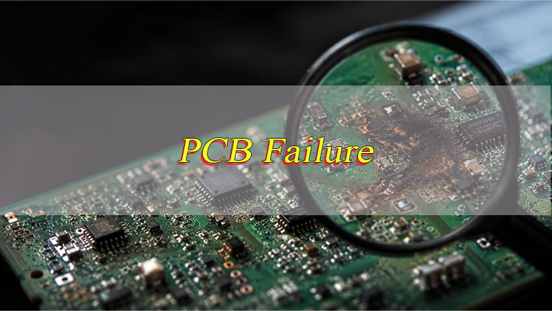
Can PCB failure stop a device even when the board looked normal during early testing? the answer is yes. A PCB may pass a basic check, but hidden problems inside copper traces, plated holes, laminate, solder mask, surface finish, or internal layers can still affect power, signal transmission, heat flow, or long-term stability.
PCB failure may come from poor layout, unsuitable materials, fabrication defects, moisture, heat, vibration, electrical overstress, contamination, or aging. Some problems appear during first testing, while others only happen after the board runs under real load for weeks or months. This guide explains common failure modes, warning signs, analysis methods, prevention steps, and how a PCB manufacturer can help reduce failure risk before production becomes costly.
What Is a PCB Failure?
A PCB failure means the printed circuit board can no longer support its intended electrical, thermal, mechanical, or insulation function. The problem may affect current flow, signal quality, heat transfer, dielectric strength, or long-term reliability.
It does not always mean the board is completely dead. Some boards still work under light load but fail when voltage, temperature, humidity, vibration, or current increases.
Common bare board problems include open traces, short circuits, weak plated holes, delamination, solder mask defects, inner-layer defects, poor insulation resistance, or incorrect copper thickness.
The difficult part is that many board failures are hidden. A PCB may look clean from the surface but still have a cracked via, internal short, weak plating, poor layer bonding, or moisture-related leakage path.
That is why PCB failure analysis should not rely on appearance alone. A reliable review should combine visual inspection, electrical testing, internal structure checks, and material evaluation when needed.
What Are Common PCB Failure Modes?
PCB failure modes describe how a board becomes unstable, unsafe, or unable to work as designed. Understanding these modes helps separate design-related, material-related, fabrication-related, and environment-related problems.
- Open circuit failure: This happens when an electrical path is broken. The break may appear in a copper trace, plated through hole, via, pad, or inner-layer connection. Common causes include copper cracking, over-etching, weak plating, pad lifting, drilling defects, or mechanical stress.
- Short circuit failure: This happens when two points that should stay separated become electrically connected. It may occur between adjacent traces, vias, pads, or internal copper layers. Short circuits may cause overheating, leakage current, or complete circuit shutdown.
- CAF PCB failure: CAF means conductive anodic filament. It is a hidden electrochemical path that can form inside the PCB laminate between nearby conductors. It is often related to moisture, voltage bias, close conductor spacing, laminate quality, and ionic contamination.
- Via and plated hole failure: Vias and plated holes connect different copper layers. If plating is too thin, cracked, or poorly bonded, the electrical connection may become unstable. A board may pass a simple room-temperature test but fail later after heat, vibration, or long-term use.
- Delamination and blistering: Delamination means the PCB layers begin to separate. Blistering is a visible surface sign. This may be caused by moisture absorption, unsuitable laminate, weak lamination quality, excessive thermal stress, or material mismatch.
- Corrosion failure: Corrosion can attack copper traces, pads, vias, and exposed metal surfaces. Humidity, ionic residue, chemical vapor, salt mist, or poor storage conditions can lead to corrosion. Over time, it may cause leakage, high resistance, open circuits, or unstable signals.
- Thermal failure: Thermal failure happens when heat cannot move away from high-current paths or heat-sensitive board areas. Weak copper design, insufficient copper thickness, poor thermal vias, or unsuitable material can increase temperature rise. Heat control should be planned during PCB design and material selection.
- Solder mask failure: Solder mask protects copper and helps maintain insulation between conductors. If it is too thin, poorly cured, misaligned, cracked, or contaminated, the board may face higher risk of leakage, corrosion, or short circuits.
What Causes PCB Failure?
PCB board failure reasons are often connected. A board may fail because several weaknesses combine, such as limited design margin, unsuitable material, unstable fabrication control, harsh environment, or incomplete testing.
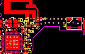
- Poor PCB layout: Trace width, copper spacing, via size, annular ring, grounding, return path, creepage distance, and heat flow all affect reliability. If a high-current trace is too narrow, it may overheat. If high-voltage spacing is too small, leakage or arcing may occur.
- Unsuitable material selection: PCB material should match the working environment. Tg, CTI, copper thickness, dielectric properties, moisture resistance, solder mask quality, and surface finish all matter. A PCB used in heat, humidity, high voltage, or outdoor equipment needs stronger material planning.
- Fabrication defects: Defects can create hidden risks before the board is used. Examples include under-plated vias, over-etched traces, poor lamination, resin voids, copper nicks, inner-layer misregistration, solder mask misalignment, or poor surface finish.
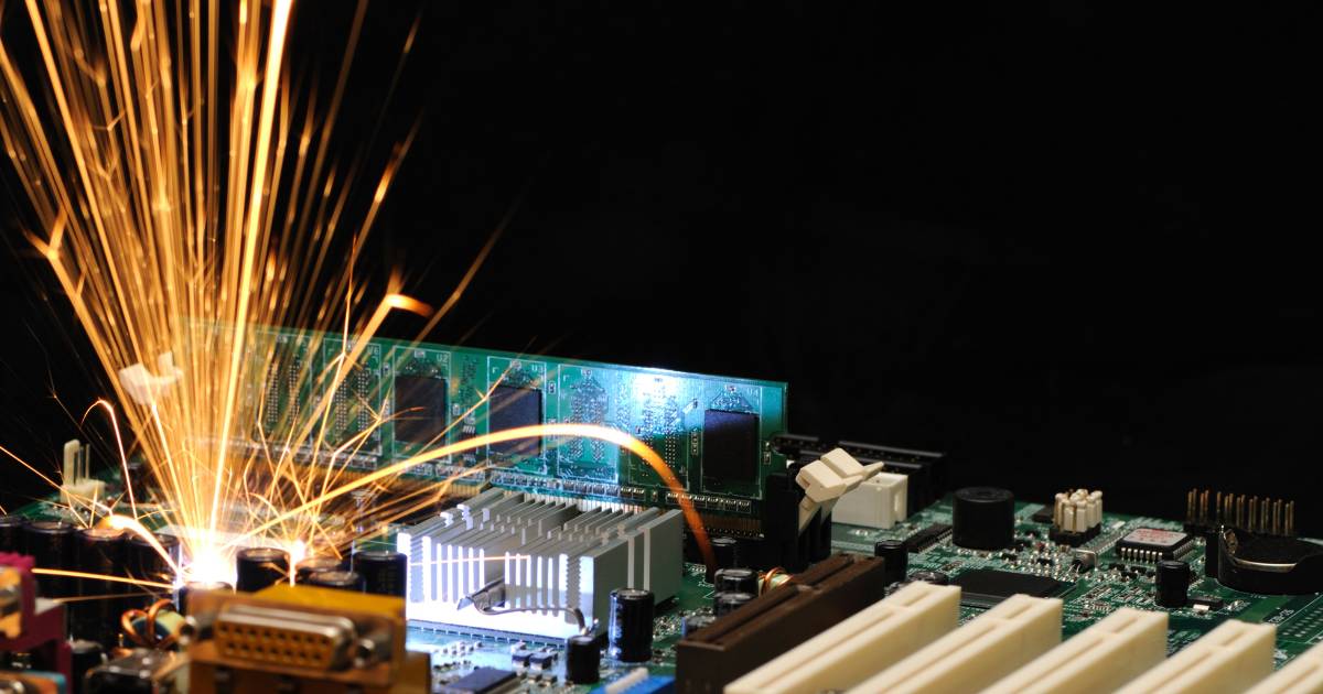
- Electrical overstress: Surge, ESD, overvoltage, overcurrent, reverse polarity, and unstable power input can damage copper paths, insulation areas, and protection zones. Some damage is visible, while some appears only after continued use.
- Heat and mechanical stress: Repeated heating and cooling can fatigue plated holes, vias, copper connections, and laminate structures. Vibration, shock, bending, connector force, and enclosure pressure can also damage copper or weaken internal connections.
- Moisture and contamination: Dust, fingerprints, ionic residue, cleaning residue, and chemical contamination can reduce insulation resistance. In serious cases, they may cause corrosion, leakage current, or CAF. Cleanliness directly affects long-term electrical stability.
- Long-term aging: During long-term service, copper surfaces may corrode, insulation may weaken, and plated holes may fatigue under repeated temperature or mechanical stress. Aging becomes faster under high temperature, high humidity, high current, vibration, or frequent power cycling.
How Do I Know If the Problem Is PCB Failure?
A device symptom does not always prove the PCB is the source of the problem. Power adapters, cables, connectors, sensors, displays, motors, software, and external loads can create similar symptoms. Still, some signs strongly suggest a board-level fault.
- No power response: If there is no response after power input, the issue may be related to an open trace, damaged power path, short circuit, weak plated hole, or poor copper connection.
- Startup and shutdown loop: Random restart, unstable booting, or shutdown after a few seconds may point to voltage drop, leakage current, overheating, poor insulation, or intermittent copper connection.
- Burn marks or discoloration: Dark FR4, melted solder mask, charred copper areas, or local discoloration usually indicates excessive current, poor heat dissipation, or electrical overstress.
- Burning smell: A burnt smell near the board surface may suggest overheating, carbonized material, damaged copper paths, or local insulation breakdown.
- Unstable signals: Communication errors, unstable output, signal drift, or random data errors may come from poor impedance control, weak grounding, cracked vias, internal connection defects, or contamination.
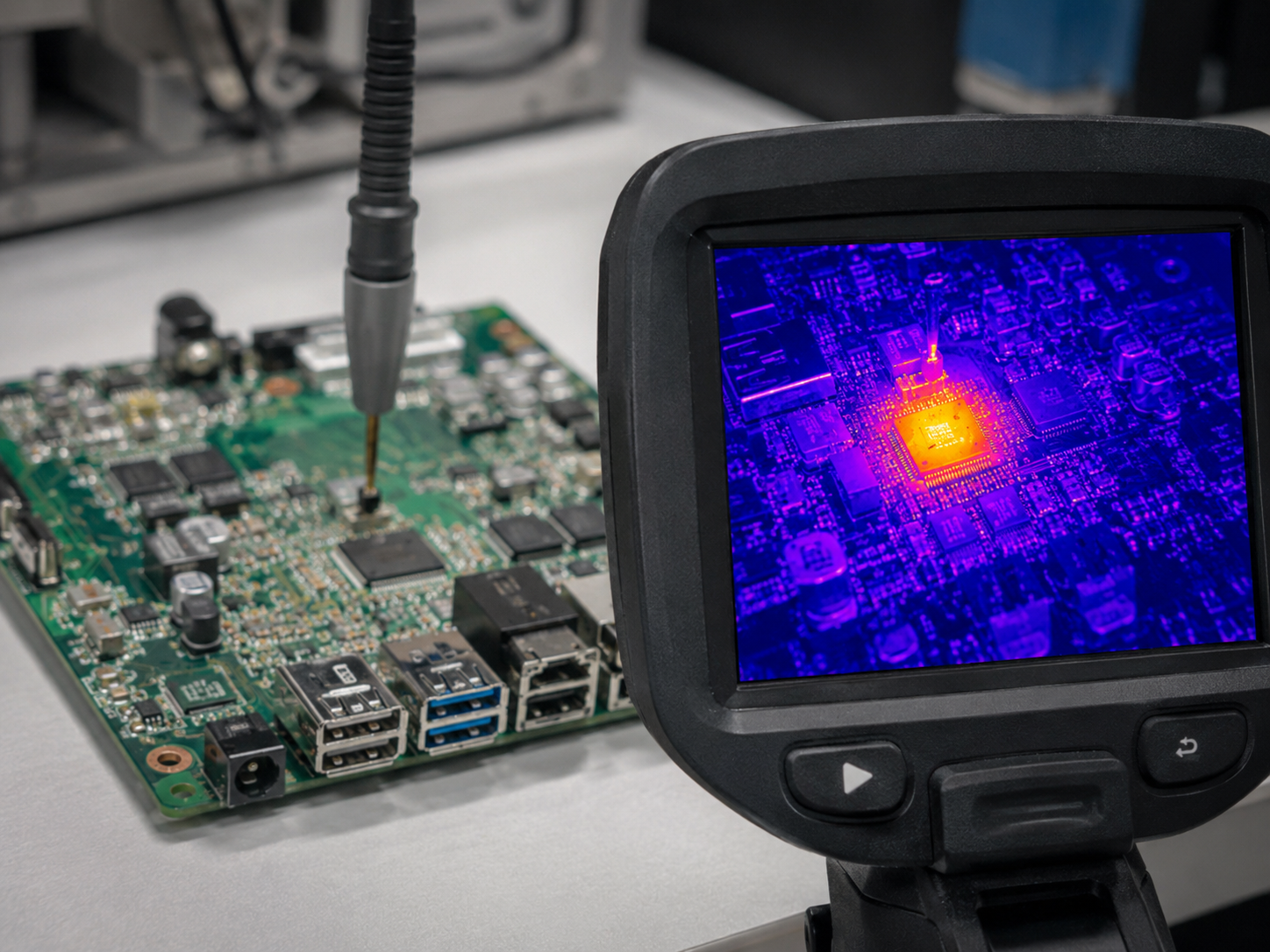
- Abnormal hot area: If one area is much hotter than the rest of the board, the fault may be near that location. Thermal imaging can help locate high-resistance paths, overloaded copper areas, or poor thermal spreading.
- Corrosion or white residue: White residue, green corrosion, darkened pads, or dull exposed metal areas may indicate moisture, ionic residue, or chemical contamination.
- Condition-based failure: If the issue appears only after warm-up, vibration, high load, or humidity exposure, it may be an intermittent PCB defect. These cases usually need deeper analysis because the board may look normal during a quick bench test.
How to Perform a PCB Failure Analysis?
PCB failure analysis should follow the evidence, not assumptions. The practical sequence is simple: confirm the symptom, inspect the board, measure electrical behavior, check hidden areas, and verify the root cause.
- Record the failure condition first: Record the board revision, batch number, working time, input voltage, load condition, failure rate, and actual symptom. A board that fails during first power-on may involve a short circuit, open trace, wrong copper spacing, or fabrication issue. A board that fails after several months may involve heat, moisture, vibration, corrosion, CAF, or aging.
- Inspect the board surface: Check the board under good lighting and magnification. Look for burn marks, lifted pads, darkened FR4, corrosion, white residue, solder mask damage, copper exposure, delamination, scratches, and board edge damage.
- Check high-risk areas first: Start with power input areas, high-current traces, high-voltage spacing, vias, plated holes, dense routing areas, board edges, and places with visible discoloration or residue.
- Measure before applying power: Use a multimeter to check resistance, continuity, insulation behavior, and power paths. This step helps find short circuits, open circuits, broken traces, damaged vias, or poor plated hole connections.
- Power the board only when safe: Increase voltage gradually and monitor current, voltage behavior, and surface temperature. A sudden current rise often suggests a short or leakage path. A hot spot may point to excessive copper resistance, poor heat spreading, insulation breakdown, or conductive contamination.
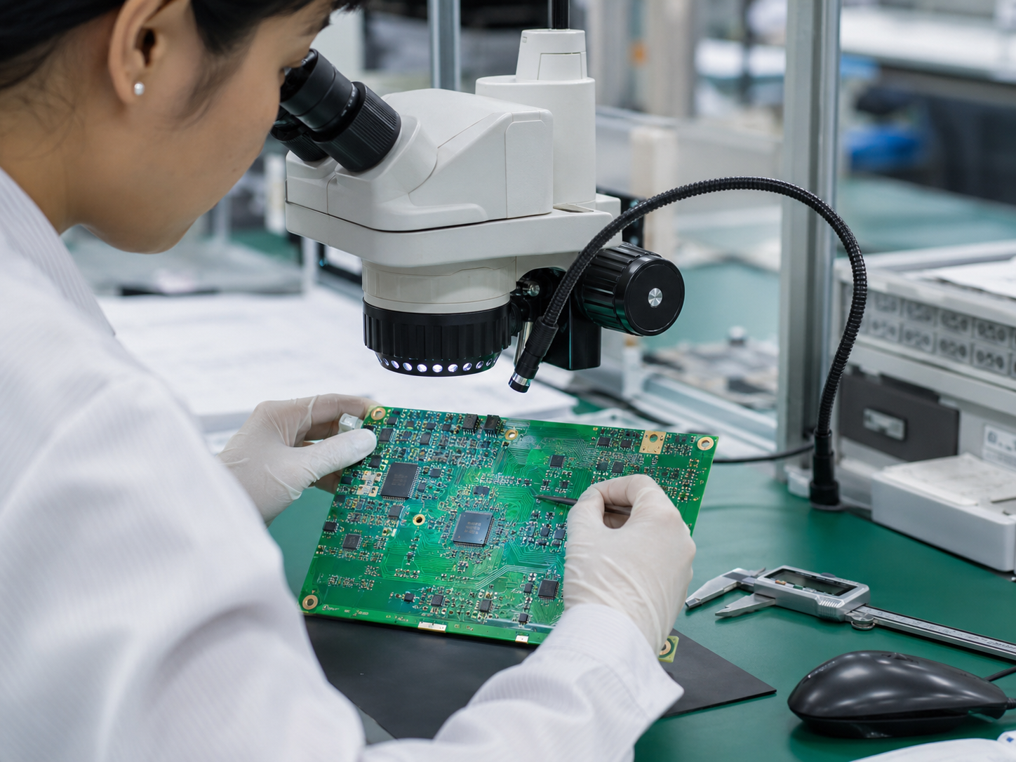
- Use magnification for small defects: A microscope can reveal fine copper defects, scratches, small residues, solder mask cracks, pad damage, and early corrosion that cannot be seen by eye.
- Use X-Ray for hidden concerns: X-Ray inspection can help check dense via areas, buried structure issues, inner abnormalities, and defects that cannot be reviewed from the surface.
- Use cross-section analysis for internal problems: Cross-sectioning can reveal thin copper plating, barrel cracks, resin voids, inner-layer separation, laminate defects, and poor hole-wall connection. It is especially useful when the PCB looks normal but fails intermittently.
- Check contamination when leakage or corrosion appears: Ionic contamination testing, SIR testing, SEM/EDS, and FTIR can help identify residue, corrosion products, chemical contamination, and metal migration. These methods are useful for boards used in humid, outdoor, automotive, and industrial environments.
- Confirm the root cause clearly: The final result should answer three questions: what failed, why it failed, and how to prevent it from happening again. Corrective action may include layout revision, material change, via structure adjustment, copper thickness adjustment, solder mask improvement, surface finish change, storage control, or stronger inspection before shipment.
What PCB Failure Analysis Techniques Are Commonly Used?
Different failure types need different analysis methods. A burnt copper path, cracked via, internal layer defect, CAF path, and corrosion problem cannot be checked with the same tool.
- Visual inspection: This checks burn marks, corrosion, scratches, lifted pads, exposed copper, board edge damage, discoloration, and visible surface defects. It should be the first check because it is fast and does not damage the board.
- Microscope inspection: This checks fine copper defects, small cracks, pad damage, solder mask defects, tiny residue, and early corrosion. It is useful for dense routing areas and small surface problems that are hard to see by eye.
- Electrical testing: This checks shorts, opens, voltage behavior, current paths, leakage, and insulation resistance. It helps confirm whether the issue is electrical, structural, or insulation-related.
- Bare board AOI: This checks trace width, spacing, copper defects, shorts, opens, and pattern accuracy. It is useful during PCB fabrication because it can find repeated process problems before shipment.
- X-Ray inspection: This helps review hidden structures, dense via areas, buried defects, and internal abnormalities. It is useful when the board surface looks normal but the electrical behavior is unstable.
- Thermal imaging: This shows hot copper areas, high-resistance paths, poor heat spreading, and abnormal temperature rise. It is useful for overheating faults and high-current board areas.
- Cross-section analysis: This checks plating thickness, via cracks, delamination, laminate voids, inner-layer connection, and hole-wall quality. This method is destructive, so it is usually used after other checks narrow down the suspected area.
- SEM/EDS analysis: This checks corrosion products, metal particles, foreign residue, and material composition. It is useful when the source of contamination or corrosion is unclear.
- SIR and ionic testing: These tests check insulation reliability, ionic residue, leakage risk, and CAF risk. They are useful for moisture-related failure, corrosion concerns, and boards used in harsh environments.
- Practical sequence: Start with simple, non-destructive checks, then move to deeper testing only when the evidence requires it. This protects useful failure evidence and avoids unnecessary destructive testing.
Can PCB Failure Be Simulated Before Production?
PCB failure simulation can reduce risk before boards are built. It cannot replace real testing, but it helps identify weak areas before fabrication begins.
- Thermal simulation: This is useful for boards with high-current traces, dense copper areas, heat-sensitive zones, and limited board space. It shows whether copper area, via quantity, board thickness, and heat-spreading path are suitable for the expected load.
- Signal and power integrity simulation: This helps review impedance, return path, crosstalk, switching noise, voltage ripple, and high-speed signal quality. It is useful for communication boards, RF boards, control boards, and compact high-density layouts.
- Mechanical stress simulation: This can predict bending, vibration, connector force, enclosure pressure, and thermal expansion mismatch. These checks are valuable for automotive electronics, industrial control modules, UAV modules, and outdoor equipment.
- High-voltage and high-current review: Spacing, creepage distance, copper width, via current capacity, and heat path should be reviewed before the board layout is released.
- Better use of simulation: Simulation works best when it is combined with DFM review, prototype testing, fabrication process validation, and electrical verification. It helps reduce repeated layout changes after production starts.
How Can PCB Failure Be Prevented?
PCB failure prevention starts before fabrication. A final test can find some defects, but it cannot fix weak layout, wrong material choice, poor heat design, unstable plating, or hidden contamination risk.
- Review the design before fabrication: Check trace width, copper spacing, via size, annular ring, solder mask clearance, creepage distance, high-current paths, high-voltage spacing, and thermal areas before releasing production files. This step catches many problems early.
- Choose materials for the real working environment: Material selection should match heat, humidity, voltage, vibration, and service life requirements. For high-temperature products, select suitable Tg and copper thickness. For high-voltage boards, review CTI, creepage, and clearance.
- Control heat from the layout stage: Use wider copper, proper copper weight, thermal vias, heat-spreading areas, and suitable copper distribution. If heat cannot leave the board, copper paths, insulation, and laminate materials may age faster.
- Reduce contamination risk: Dust, fingerprints, chemical residue, moisture, and ionic contamination can cause corrosion, leakage current, or CAF over time. Use clean handling, proper storage, controlled production conditions, suitable cleaning requirements, and moisture control.
- Control PCB fabrication parameters: Drilling, desmear, plating, imaging, etching, lamination, solder mask, and surface finish must be controlled within stable process windows. Stable fabrication reduces open circuits, short circuits, under-plated holes, over-etched traces, weak insulation, and solder mask defects.
- Use testing that matches the board risk: A simple board may only need visual inspection and electrical testing. A dense, high-current, high-speed, or high-reliability board needs stronger inspection. Common choices include bare board AOI, electrical test, flying probe, impedance testing, ionic contamination testing, cross-section checks, thermal review, and reliability testing.
- Keep traceability records: Record PCB lot, laminate batch, copper thickness, surface finish, fabrication process data, inspection result, and test report. When a problem appears later, traceability helps narrow the cause quickly.
- Use trial builds before volume production: A trial build can expose heat concentration, weak spacing, plating risk, panelization issues, warpage risk, and test coverage gaps. After the trial build, update the layout, stackup, material selection, process settings, inspection method, or test requirement before volume production starts.
How Does a PCB Manufacturer Support Failure Reduction?
A PCB manufacturer can reduce many risks before boards reach final use. This is especially important for products with compact layout, high current, high voltage, high speed, strict reliability needs, or harsh working environments.
- DFM and file review: A PCB manufacturer can review Gerber files, stackup, drill design, copper spacing, solder mask, surface finish, impedance features, panelization, and tolerance requirements before production.
- Material and stackup guidance: The manufacturer can suggest suitable FR4, high Tg laminate, high-frequency material, metal core PCB, ceramic PCB, heavy copper PCB, or rigid-flex construction based on working conditions.
- Controlled PCB fabrication: Stable lamination, drilling, plating, imaging, etching, solder mask, surface finish, and electrical testing help reduce hidden bare board defects.
- Process inspection and testing: Bare board AOI, electrical testing, flying probe testing, impedance testing, cross-section checks, microsection review, and reliability testing can help detect many problems before shipment.
- Failure review support: When a problem appears, a PCB manufacturer can compare design files, material records, fabrication data, inspection results, test data, and batch history to support root cause analysis.
- Prototype to volume production support: Trial builds help refine material selection, stackup, copper design, via structure, impedance control, inspection standards, and test plans before the same issue repeats in a larger batch.
FAQs About PCB Failure
Q1: What is main PCB failure?
A1: Main PCB failure means the primary control board in a device cannot support its power distribution, communication, or signal control function correctly. It may cause no power, startup failure, display error, control fault, or communication loss.
Q2: What are signs of 4R70W PCB board failure?
A2: In a 4R70W transmission-related circuit board, possible signs may include shift irregularity, electrical fault codes, sensor signal errors, or control problems. Wiring, connectors, sensors, and related control circuits should be checked together before confirming board damage.
Q3: What are hard drive PCB failure symptoms?
A3: Common hard drive PCB failure symptoms include no spin, no power response, burning smell, visible burn marks, drive not detected, or repeated clicking after power-on. Board replacement is not always simple because firmware or ROM data may need to match the original drive.
Q4: Why does CAF happen inside a PCB?
A4: CAF can happen when moisture, voltage bias, weak glass fiber interface, close conductor spacing, and ionic contamination appear together inside the laminate. It is more likely in dense via areas, fine conductor spacing, and high-humidity working conditions.
Q5: Can X-Ray find every board fault?
A5: No. X-Ray is useful for hidden structures, dense via areas, internal abnormalities, and some buried defects. However, it cannot replace electrical testing, microscope inspection, cross-section analysis, or contamination testing.
Q6: How long does board-level analysis take?
A6: Simple visual or electrical faults may be identified quickly. Complex cases involving CAF, intermittent faults, thermal cycling, corrosion, or cross-section testing need more evidence and a controlled analysis process.
Conclusion
Want to reduce PCB fault risks before production starts? Send your Gerber files and project requirements to EBest for a free DFM analysis. Our team can review layout risks, material selection, stackup, copper spacing, via design, solder mask clearance, and manufacturability before fabrication, helping you prevent hidden PCB problems and move into production with more confidence. And we provide a full range of PCB manufacturing services, including FR4 PCB, MCPCB, ceramic PCBs and others PCBs. Contact us for a quotation at sales@bestpcbs.com.