PCB manufacturing PCB manufacturing
Home > Blog

Custom Number Pad PCB Manufacturer for USB-C, Hot-Swap and Wireless Designs

July 28th, 2026

A custom number pad PCB combines the key-switch circuit, controller, interface and optional lighting or wireless functions in a board shaped for a specific keypad. Releasing it for production requires four matching elements: switch footprints aligned with the plate and enclosure, firmware mapped to the matrix, a verified USB or wireless interface, and repeatable functional-test criteria.

EBest Circuit supports custom number pad PCB prototyping, fabrication and assembly for projects that need USB-C, hot-swap sockets, programmable keys or wireless functions. Send your layout, Gerber files, BOM, firmware requirements, mechanical drawings and order quantity to sales@bestpcbs.com for a manufacturability review and quotation.

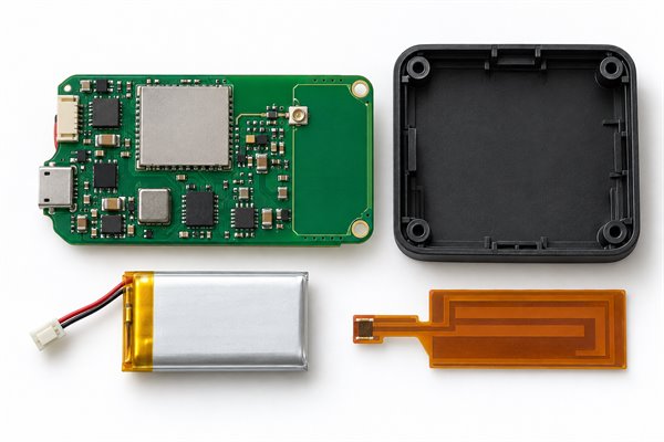
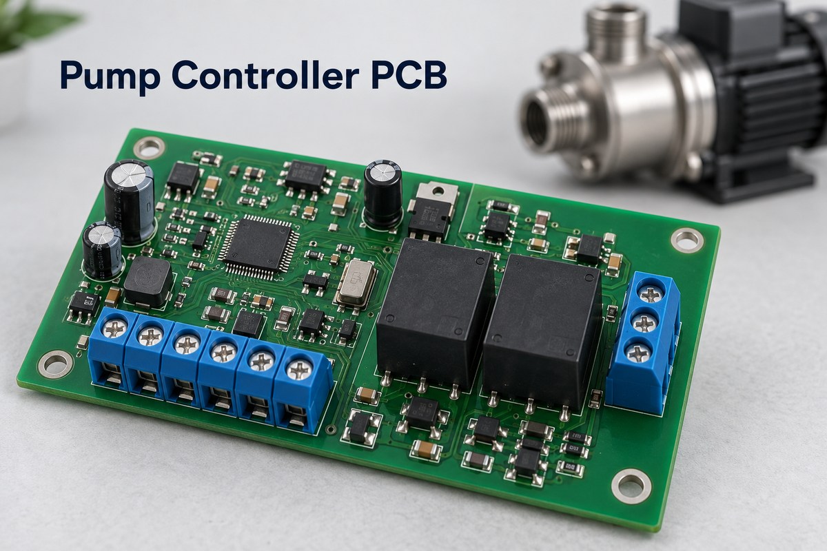
Custom number pad PCB with USB-C connector, hot-swap sockets and assembled components

What Is a Custom Number Pad PCB and How Does It Work?

A custom number pad PCB detects key presses through a switch matrix, converts them into commands and sends those commands to a computer or host system. The board can be a simple wired numeric keypad, a programmable macro pad, a wireless data-entry device or part of an industrial control panel.

Most designs arrange switches into rows and columns. When a key closes, the controller identifies the connected row and column. A diode at each switch controls current direction and reduces ghosting when several keys are pressed. Firmware then maps that switch position to a number, command, shortcut or macro.

The PCB locates switches, stabilizers, LEDs, encoders, displays, connectors and mounting holes. Electrical and mechanical design must therefore be checked together: a working circuit can still fail assembly if the USB connector misses the enclosure opening or a socket collides with a mounting boss.

During a key scan, the controller drives one matrix line at a time and reads the others. Firmware filters contact bounce, applies the selected key map and sends the resulting USB or wireless report. This signal path creates four separate verification points: switch continuity, diode direction, matrix coordinates and host output. Checking all four makes it possible to distinguish a soldering fault from a routing or firmware error.

Which Custom Number Pad PCB Type Fits Your Application?

Custom number pad PCBs are best classified by system architecture: wired fixed-function, wired programmable, wireless programmable or host-integrated industrial. Hot-swap sockets are a switch-mounting option that can be added to wired or wireless programmable designs, not a separate PCB class.

System Architecture Host Connection Control and Switch Options Best Fit Main Trade-Off
Wired fixed-function USB-C or fixed cable Preset key map; soldered switches are typical Stable numeric entry with no user remapping Simple to control, but later function changes require firmware or hardware revision
Wired programmable USB-C QMK, VIA or custom firmware; soldered or hot-swap switches Macros, layers, shortcuts and configurable input Requires controller compatibility, programming access and firmware control
Wireless programmable Bluetooth or other selected radio Programmable control; soldered or hot-swap switches Portable or cable-free products Adds antenna, battery, charging, sleep-current and regulatory requirements
Host-integrated industrial USB, serial or host-specific interface Fixed or programmable functions matched to the host system Equipment panels, terminals and access-control interfaces Connector retention, ESD strategy and acceptance tests are application-specific

Choose the architecture first, then specify soldered or hot-swap switches, lighting, encoders and displays as options within that architecture. This prevents overlapping features from being treated as incompatible PCB types.

What Should Be Defined Before Starting a Custom Numpad PCB Design?

Define the product requirements before drawing the schematic because key count, layout, connection, firmware and enclosure decisions control the entire board. A written input sheet prevents late changes that alter footprints, controller pins, board outline or assembly cost.

  1. Lock the key layout. Record the number of keys, key-unit spacing, rotated switches, stepped keys, 2U keys and any nonstandard left-hand arrangement.
  2. Select the switch system. Define soldered or hot-swap switches, switch family, plate-mounted or PCB-mounted construction and required stabilizers.
  3. Define user functions. List numeric input, shortcuts, layers, custom macros, rotary encoders, displays, RGB lighting and status indicators.
  4. Choose the connection. State whether the product uses USB-C, a fixed cable, Bluetooth or another host interface.
  5. Set the power architecture. Identify USB power, battery type, charging method, sleep behavior and the maximum expected LED load.
  6. Freeze the mechanical envelope. Provide the board outline, mounting points, connector opening, plate file, enclosure model and maximum component heights.
  7. Define firmware ownership. Confirm who supplies the source code, compiled firmware, key map, bootloader and programming instructions.
  8. Define production acceptance. Specify which electrical, programming, key, LED, wireless and current tests determine whether an assembled board passes.

How Should a Custom Number Pad PCB Switch Matrix Be Designed?

Design the switch matrix from the physical key map, required simultaneous-key behavior, available GPIO pins and firmware scan direction. A 4 × 5 matrix supports 20 positions with nine row-and-column signals, reducing pin use compared with direct wiring while keeping each key individually identifiable.

  1. Create a physical key map. Give every switch a reference designator and record its row, column, key size and firmware position. Include encoders, layer keys and any alternate-layout positions so no input is assigned only in firmware.
  2. Choose practical matrix dimensions. Select row and column counts that fit the controller’s available GPIO pins and produce clear routing. Compare candidate arrangements before fixing the schematic; a balanced matrix is not useful if it creates long crossings around the connector, LEDs or mounting holes.
  3. Confirm the scan direction. Decide whether firmware drives columns and reads rows or drives rows and reads columns. Use the same direction in the schematic net names, diode orientation and firmware configuration.
  4. Use one diode per key for multi-key operation. Per-key diodes prevent unintended current paths when several switches close at once. Match the diode footprint polarity mark, assembly drawing and firmware setting so correctly soldered parts cannot be installed in the wrong direction.
  5. Separate matrix and lighting circuits. Keep row and column routes away from LED power switching, high-current RGB paths and noisy regulators where practical. Provide stable return paths and follow the controller reference design for pull resistors, reset and interface protection.
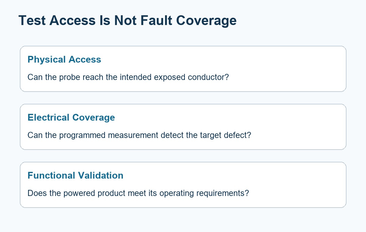
  6. Provide diagnostic access. Add accessible row, column, power, reset and programming points when fixture testing or fault isolation is required. Test access allows an open switch, reversed diode or broken matrix trace to be located without probing under installed switches.
  7. Control debounce and scan behavior in firmware. Verify that the scan rate, debounce method, layer handling and simultaneous-key behavior match the intended use. Test normal typing, held keys, rapid repeated input and required key combinations on the assembled prototype.
  8. Cross-check all released files. Compare switch references, net names, matrix coordinates, diode direction and controller pins across the schematic, PCB and firmware definition. Generate a matrix verification sheet that states the expected host output for every physical key.

Typical failures include swapped key positions, a complete dead row or column, ghost inputs and keys that work only in one firmware build. Diagnose them in order: check switch continuity, diode polarity, row and column continuity, controller pin assignment and final key-map output. This sequence separates assembly defects from PCB routing and firmware errors.

How Should USB-C and Wireless Connectivity Be Designed for a Custom Numpad PCB?

USB-C and wireless designs require different power, protection, placement and test plans. USB-C prioritizes connector anchoring, correct USB-C pin configuration, ESD protection and data routing. Wireless designs add antenna clearance, battery safety, charging control and low-power firmware.

USB-C Numpad PCB Design

  • Define the USB-C device role. A typical wired numpad is a USB 2.0 peripheral that receives 5 V from the host, so configure it as an upstream-facing port and power sink. Unless a USB-C or power-delivery controller requires another implementation, connect separate 5.1 kΩ Rd pull-down resistors from CC1 and CC2 to ground so the numpad is detected in either plug orientation. Do not use Rp pull-ups, which advertise a power-source role.
  • Join the duplicated USB 2.0 contacts correctly. On a full USB-C receptacle, connect A6 and B6 to the same D+ net and A7 and B7 to the same D− net close to the connector, then route D+ and D− as one differential pair to the controller. Verify the exact receptacle pinout because connector symbols and reduced-pin USB 2.0 receptacles can differ.
  • Control the connector mechanically. Position the receptacle from the final enclosure datum. Verify shell tabs, locating posts, insertion direction, cable clearance, board-edge distance and support against repeated cable force.
  • Protect power and data lines. Place suitable ESD protection close to the receptacle, provide a defined shield connection and size the VBUS path for the intended current. Keep protection-device stubs and the D+/D− route short.
  • Route the data pair consistently. Keep D+ and D− together over a continuous reference path, minimize branch length where the duplicated contacts join, avoid unnecessary vias and do not cross plane gaps. Review the controller reference design, receptacle breakout and ESD-device layout before fixing the route.
  • Verify the assembled interface. Test enumeration, every key function, cable movement and connector alignment with the final firmware and representative enclosure. A continuity check alone cannot confirm stable host communication.

Wireless Numpad PCB Design

  • Select the radio architecture. Confirm the controller or module, supported firmware, antenna type, programming method and target-market requirements before layout. Module approval does not remove the need to review the final antenna implementation and product configuration.
  • Protect the antenna area. Follow the radio supplier’s keepout dimensions and placement guidance. Keep copper, batteries, displays, cables, metal fasteners and enclosure features out of restricted antenna regions.
  • Design the complete power path. Match battery chemistry, protection, charging circuit, connector and charge current. Calculate active, LED-on, sleep and charging current separately so firmware power states and expected operating time can be evaluated.
  • Plan battery and enclosure integration. Verify battery space, cable routing, service access, heat sources and mechanical retention in the 3D assembly. The enclosure material and nearby metal parts can change radio performance.
  • Test the finished wireless product. Check pairing, reconnection, input response, operating range, sleep current and charging behavior with the intended battery and enclosure. Open-board range is not representative of the final assembly.

How Can a Programmable Custom Number Pad PCB Support QMK, VIA and Custom Macros?

A programmable custom number pad PCB needs a supported controller, correct matrix definition, sufficient firmware resources and a controlled programming process. QMK can implement layers, tap functions, rotary encoders and custom key behavior. VIA can allow compatible key maps to be changed without rebuilding firmware, while application-specific macros can be implemented in firmware or host software.

  • Controller support: verify that the selected microcontroller, bootloader and available pins match the intended firmware before finalizing the PCB.
  • Matrix definition: keep row pins, column pins, diode direction and physical layout consistent across the schematic, PCB and firmware files.
  • Programming access: provide an accessible reset or boot method and the pads or connector required by the chosen programming process.
  • Version control: identify the firmware filename, version, checksum and approved key map on the production package.
  • Functional limits: confirm memory use, LED current, encoder behavior, sleep mode and wireless functions on the actual assembled prototype.

The production package should contain the approved compiled file, version, checksum, programming voltage, access location and readback method. Assign each key-map variant a distinct part number or configuration code. Test macros that depend on host software, operating-system permissions or timing in the target environment; continuity testing cannot detect an incorrect pin map or bootloader.

How Should Hot-Swap Socket, Switch and Stabilizer Clearances Be Set?

Clearances must be checked as a complete mechanical stack that includes the PCB, socket, switch, plate, stabilizer, enclosure and nearby components. A correct schematic symbol does not prove that a hot-swap socket can be soldered, that a switch will seat fully or that a stabilizer will move without interference.

  1. Use the approved socket footprint. Confirm pad shape, socket orientation, switch-pin holes and manufacturer drawing against the selected part number.
  2. Check the underside keepout. Prevent sockets from colliding with mounting posts, batteries, controller modules, connectors or enclosure ribs.
  3. Confirm stabilizer format. Match PCB-mounted or plate-mounted stabilizers to the plate cutout, switch position and large-key orientation.
  4. Verify plate-to-PCB spacing. Model the switch, plate, PCB and any foam or gasket that changes seating depth.
  5. Protect solder joints. Avoid flexing the PCB during switch insertion and removal, and review pad support around sockets near the board edge.
  6. Inspect with a 3D assembly. Overlay the PCB model, plate drawing and enclosure before prototype release, then physically test representative keys on the first assembly.

Use dimensions from the selected socket, switch and stabilizer drawings instead of a visually similar library footprint. The mechanical review should include solder-joint access, tool access for rework and the direction of force during switch replacement. On the first assembled unit, inspect representative center and edge sockets before installing all switches; edge locations often experience the greatest board flex.

Hot-swap custom number pad PCB showing switch socket, stabilizer and enclosure clearance

Which PCB Materials, Layer Counts and Surface Finishes Suit a Mechanical Numpad PCB?

FR-4 is the normal starting material, while layer count and surface finish should follow routing, wireless, connector and assembly needs. A simple wired matrix can often be routed on two layers. Four layers can provide cleaner power and ground distribution when the board adds dense lighting, a wireless module, a display or more demanding routing.

Construction Choice When It Fits Main Benefit Main Trade-Off What to Confirm
Two-layer FR-4 Basic wired matrix and moderate component count Simple, economical construction Less routing and plane flexibility Ground return paths and connector routing
Four-layer FR-4 Wireless, dense RGB, display or compact routing Dedicated plane options and easier routing control Higher fabrication cost than two layers Final stackup and antenna requirements
HASL finish General through-hole or larger-pitch assembly Common and practical Surface planarity is less uniform than ENIG Fine-pitch pads and socket assembly needs
ENIG finish Fine-pitch parts, flat pads and mixed assembly Flat solderable surface Higher cost than common HASL options Project storage and assembly requirements
OSP finish Flat copper pads with a defined assembly flow Flat surface with a thin coating Handling and storage controls matter Assembly timing and rework plan

EBest Circuit’s general PCB capability workbook lists standard FR-4 production from 1 to 10 layers, with 8-layer and higher standard builds requiring high-Tg material. It lists 10 to 32 layers as a special process range. For a number pad, extra layers should solve a real routing, plane or wireless requirement rather than serve as a generic quality upgrade.

Board thickness is also a mechanical input because it affects switch seating, USB connector alignment, stiffness and the available space below the plate. Copper weight should follow current and routing needs rather than be increased by default. Select the surface finish with the smallest assembled pads and planned storage interval in mind, then confirm solder-paste design and reflow compatibility for fine-pitch USB parts, LEDs and hot-swap sockets.

What Should Be Verified on a Custom Number Pad PCB Prototype?

A custom number pad PCB prototype must verify electrical operation, mechanical fit, firmware behavior and the proposed production test, not merely power on. Approval should use a written checklist so that a repaired sample does not become the undocumented reference for later production. This validation sequence complements the broader controls used for a fast-turn PCB prototype.

  1. Inspect the bare board. Confirm outline, slots, mounting holes, connector position, surface finish, solder mask openings and identification marks.
  2. Check assembly orientation. Verify diodes, controller, USB components, LEDs, sockets, encoders and polarized parts against the assembly drawing.
  3. Power the board safely. Check for shorts and abnormal current before connecting the complete product.
  4. Program the approved firmware. Record the build version and verify that the boot or reset method remains accessible.
  5. Test every input. Exercise all keys, layers, macros, encoders and special functions, including combinations that could reveal ghosting or mapping errors.
  6. Verify the interface. Test USB enumeration and cable movement, or wireless pairing, reconnect behavior and current consumption as applicable.
  7. Assemble the mechanics. Fit the PCB with the final plate, switches, stabilizers, keycaps, enclosure and battery to identify interference.
  8. Close all deviations. Update Gerber, BOM, drawings, firmware and revision records before approving low-volume production.

Record the result for every checklist item instead of using a single “prototype passed” decision. The approval record should identify the PCB revision, BOM revision, firmware checksum, enclosure revision and any rework performed. A repaired unit may prove the proposed correction, but repeat production should use updated source files and a clean build rather than rely on undocumented jumper wires or component changes.

How Are Custom Number Pad PCBs Manufactured and Assembled?

Production converts the released data package into bare boards, assembled PCBAs, programmed units and test records through a controlled sequence. The exact route depends on whether the design combines SMT electronics, through-hole switches, hot-swap sockets, controller modules, displays or manual hardware.

  1. Review the data package. Check Gerber or ODB++, drill files, stackup, BOM, centroid data, assembly drawings, firmware and acceptance criteria.
  2. Complete DFM and DFA review. Identify footprint, polarity, clearance, panelization, solder-mask, test-access and mixed-assembly risks before release.
  3. Prepare the production panel. Select panel rails, tooling holes, fiducials and routing or V-cut methods that support assembly and depanelization.
  4. Fabricate the bare PCB. Process imaging, etching, drilling, plating, solder mask, legend, surface finish, profiling and electrical testing under the approved construction.
  5. Source and verify components. Match manufacturer part numbers, packages and approved alternatives, with special attention to controllers, USB connectors, radio modules and hot-swap sockets.
  6. Assemble SMT components. Print solder paste, place components, reflow and inspect the board before operations that reduce access.
  7. Complete through-hole and manual assembly. Install switches, headers, encoders, modules or connectors according to the approved route.
  8. Program, clean and test. Load the approved firmware, inspect workmanship and run the specified electrical and functional tests before packing.

Sequence the operations around access and heat exposure. Fine-pitch USB parts, controllers and LEDs are normally inspected before large switches, sockets or modules restrict the view. Manual operations need defined orientation and solder criteria, while programming must use the released firmware identity. Final cleaning requirements depend on the flux and assembly route, and completed boards should be protected against connector or switch damage during packing.

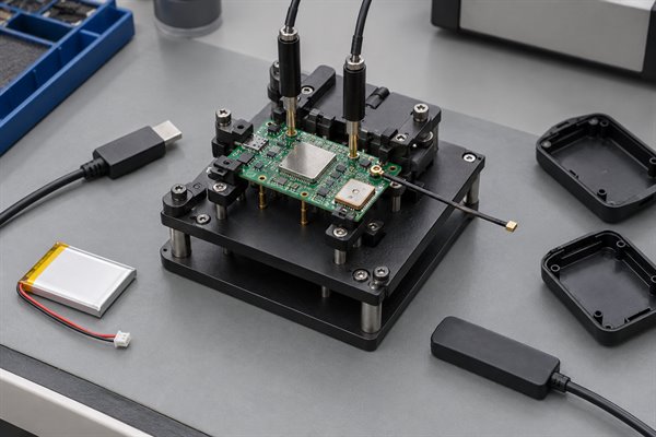
Custom number pad PCBA assembly and functional key testing process

What Changes When a Custom Number Pad PCBA Moves to Low-Volume Production?

Low-volume production replaces prototype flexibility with documented materials, fixtures, test limits and revision control. The objective is to reproduce the approved behavior without relying on manual knowledge from the first build.

Control Point Prototype Build Low-Volume PCBA Reason for the Change
BOM Parts may be purchased in small quantities Manufacturer part numbers and approved alternates are frozen Prevents uncontrolled substitutions
Panelization Single boards may be acceptable Panel format supports placement, handling and depanelization Improves repeatability and throughput
Programming Manual loading may be used Firmware file, version and work instruction are controlled Prevents mixed firmware
Testing Bench checks may find obvious faults Fixtures or repeatable procedures apply defined pass limits Creates consistent acceptance
Change control Rework may be exploratory All changes update design files, BOM, firmware and revision marks Keeps repeat orders traceable

Approve a golden sample or equivalent reference, close every prototype deviation and verify the panel, assembly sequence, programming and test method in a short pilot batch. Track failures by cause. Any component alternate must be checked for footprint, pinout, firmware, electrical behavior and height, then recorded across the affected fabrication, BOM, placement, drawing, firmware and test files.

Which Tests Should a Custom Number Pad PCBA Pass?

A reliable test plan must prove board integrity, correct programming and the behavior of every user input and interface. Test coverage should reflect the actual product configuration rather than apply the same generic checklist to wired, wireless and RGB designs.

Test Stage What Is Checked Typical Failure Found Acceptance Evidence
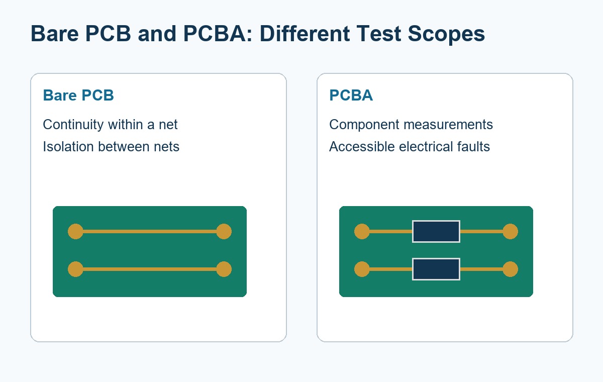
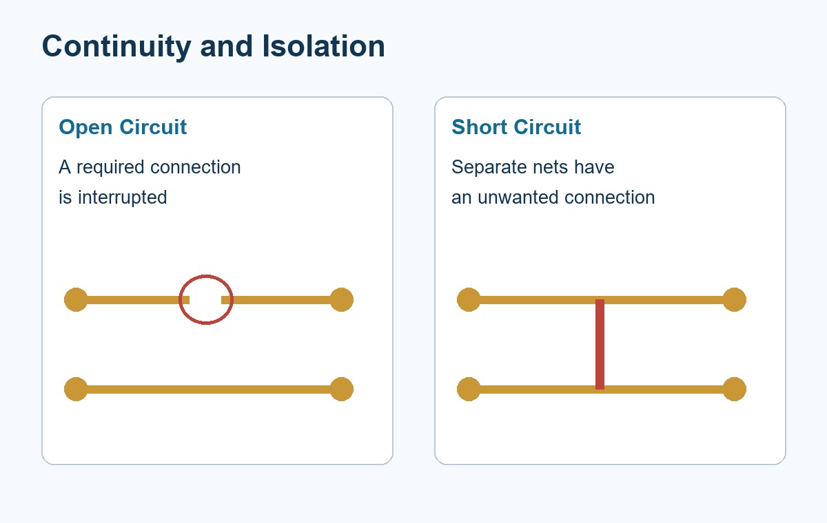
Bare-board electrical test Continuity and isolation of PCB nets Open or short circuit Electrical test result for the fabricated board
Visual or automated inspection Polarity, placement and solder-joint condition Missing, shifted, reversed or poorly soldered part Inspection result under the agreed assembly criteria
Programming verification Firmware identity and successful loading Wrong build, failed programming or inaccessible boot mode Recorded firmware version or checksum
Matrix and full-key test Every switch position and key combination Open key, swapped position, wrong diode or ghosting Pass record for all defined inputs
Interface test USB enumeration or wireless pairing and reconnect Unstable connection or interface configuration error Functional connection result
Feature test LEDs, encoders, display, macros and layers Wrong mapping, color, direction or function Approved function checklist

For wireless designs, add operating, sleep and charging-current checks with the intended battery system. For USB-C designs, test enumeration and physical connector behavior with the representative enclosure. Environmental or lifecycle testing should be defined only when the final application’s risk and service conditions require it.

Each test needs a defined setup, expected result and disposition rule. “Key works” is insufficient when the required output, layer or macro is unclear. Map every physical position to its expected report and log failed coordinates. For hidden socket or connector joints, decide during DFM whether electrical coverage, X-ray inspection or a mechanical check is required.

What Determines Custom Number Pad PCB Cost and Lead Time?

Cost and lead time depend on board construction, component availability, assembly mix, firmware handling, test coverage and order quantity. A small PCB is not automatically a simple PCBA if it contains a scarce controller, fine-pitch USB components, hot-swap sockets, a display and manual through-hole work.

  • PCB construction: layer count, board thickness, copper weight, surface finish, outline complexity and panel utilization affect fabrication.
  • Component sourcing: controller, radio module, connector, hot-swap socket and display availability can control the schedule.
  • Assembly route: SMT, through-hole soldering, hand-installed modules and mechanical hardware require different operations.
  • Programming: custom firmware, bootloader handling, serialization or multiple variants add preparation and control work.
  • Testing: full-key fixtures, wireless checks, LED inspection and current measurements add coverage but reduce escaped defects.
  • Quantity and variants: several layouts, colors or firmware versions can split material and setup across smaller batches.
  • File readiness: unresolved footprints, missing centroid data or unclear substitutions delay review and quotation.

Compare quotations by separating bare PCB, components, assembly, programming, testing and one-time tooling. Cost can often be reduced by consolidating variants, using available packages, improving panel utilization and standardizing firmware and testing. Lead time is most exposed to controllers, radio modules, displays and special connectors, so approve suitable alternatives before sourcing begins.

What Files Are Needed for a Custom Number Pad PCB Quote?

A complete quote package should describe the bare PCB, every assembled part, mechanical interfaces, firmware and test expectations. Missing information forces assumptions that can change price, schedule or deliverable scope later.

  • PCB fabrication data: Gerber or ODB++ files, NC drill files, board outline, layer count, thickness, copper weight, solder-mask color, legend and surface finish.
  • Bill of materials: reference designators, quantity, manufacturer name, manufacturer part number, package and approved alternatives.
  • Placement data: centroid or pick-and-place file with side, X/Y position and rotation.
  • Assembly drawings: polarity, do-not-fit parts, socket orientation, connector details and manual assembly notes.
  • Mechanical files: plate drawing, enclosure model, mounting points, connector opening and height limits when fit is part of the review.
  • Firmware package: approved binary, version, programming method, boot instructions and required configuration data.
  • Test requirements: full-key map, USB or wireless behavior, LED and encoder functions, current limits and required records.
  • Commercial inputs: prototype quantity, low-volume quantity, target schedule, delivery location and required packaging.

All files should carry the same revision and use consistent reference designators. The BOM must distinguish customer-supplied, manufacturer-sourced and do-not-fit parts, while the placement file must match the assembly side and board origin used in the drawings. If the quotation includes programming or functional testing, provide executable files and expected outputs, not source code alone.

How Should You Compare Custom Keypad PCB Manufacturers and Suppliers?

Compare suppliers by the controls included in the quoted scope and the evidence they can return, not by the total price alone. Use the following checks to identify omitted work, uncontrolled substitutions and test gaps before selecting a source.

  • Review the DFM and DFA scope. Ask whether the review covers footprints, solder-mask openings, hot-swap socket orientation, stabilizer and enclosure clearances, connector access, panelization and test access. Strong evidence is a marked review tied to your submitted revision; a generic “files are manufacturable” response does not show which risks were checked.
  • Confirm component control. Require manufacturer part numbers for the controller, USB connector, radio module, LEDs, sockets and other function-critical parts. Proposed alternatives should need approval after pinout, package, electrical rating, height and firmware impact are checked.
  • Define every assembly operation. Identify which party handles SMT, through-hole soldering, hot-swap sockets, switches, encoders, displays, headers and mechanical parts. This prevents a low quotation from excluding manual operations that are essential to the finished unit.
  • Verify programming responsibility. State who supplies the binary, bootloader and configuration files; how the approved version is identified; and whether programming success is read back. Request a record containing the firmware version or checksum when traceability is required.
  • Specify functional-test coverage. Confirm whether testing covers every key position, layers, macros, encoders, LEDs, USB enumeration or wireless pairing, and current measurements. Agree on the fixture, pass limits and result format instead of accepting “functional test included” without a test definition.
  • Check prototype-to-production control. Ask how prototype rework, BOM changes and firmware corrections are transferred into repeat orders. Strong control keeps Gerber, BOM, placement, assembly drawing, firmware and test revisions aligned with the approved sample.
  • Separate one-time and recurring costs. Request individual lines for bare PCBs, components, assembly, programming, testing, fixtures, tooling and customer-supplied-part handling. Quotations are comparable only when they cover the same operations and deliverables.
  • Review sample evidence. Before ordering, request one representative DFM response and one test-record example with confidential details removed. The format should show that issues, revisions, pass limits and results can be recorded clearly.

Why Choose EBest Circuit as Your Custom Number Pad PCB Manufacturer?

EBest Circuit reviews the PCB data, BOM, mechanical constraints, firmware and test requirements together, helping prevent late footprint changes, unapproved substitutions and missing assembly operations. The quotation can then identify included fabrication, sourcing, programming, manual assembly and testing work before the order is released.

  • Reduce avoidable revisions: free DFM review can identify footprint, spacing, panelization, connector and assembly concerns before fabrication.
  • Simplify project coordination: PCB fabrication, component sourcing, SMT assembly, through-hole work, programming and functional testing can be evaluated within one project package.
  • Protect BOM intent: manufacturer part numbers and proposed alternatives can be reviewed before substitution, reducing pinout, package and firmware risks.
  • Improve prototype decisions: the review can connect design files, plate and enclosure constraints, firmware and test expectations instead of checking the bare board alone.
  • Prepare for repeat orders: controlled Gerber, BOM, assembly drawing, firmware and test revisions help keep later low-volume batches aligned with the approved design.
  • Match capability to the project: standard and special PCB processes are separated during review so nonstandard construction is confirmed rather than assumed.

Submit the fabrication package, BOM, placement data, mechanical constraints, firmware and acceptance checklist together. EBest Circuit can identify missing inputs and special-process requirements before prototype or low-volume release.
FAQs About Custom Number Pad PCBs

Q1: Are per-key RGB lighting and RGB underglow the same feature?

A1: No. Per-key RGB places an LED at each switch, while underglow places LEDs on the PCB underside to illuminate the case or desk surface. They use different footprints, optical paths and power budgets, so the required lighting effect must be stated before layout.

Q2: Can one numpad PCB support both 1U and 2U key positions?

A2: It can when alternate switch holes, hot-swap sockets and stabilizer locations do not conflict. Each supported arrangement needs a defined plate and assembly variant; otherwise an electrically valid option may be impossible to assemble.

Q3: Does a hot-swap PCB automatically support every alternate layout?

A3: No. A hot-swap socket fixes the switch position and orientation, so overlapping layouts may require separate PCB variants or soldered positions. Layout support must be confirmed from the exact footprint and plate combination, not from the term “hot-swap.”

Q4: Does a USB-C daughterboard make a numpad PCB compatible with any enclosure?

A4: No. A daughterboard separates the USB opening from the main PCB, but it does not make the main PCB universally enclosure-compatible. Compatibility still depends on the board outline, mounting pattern, internal height, cable path, daughterboard location and case fastening method.

Q5: Can soldered and hot-swap versions use the same firmware file?

A5: Sometimes, if both versions use the same controller pins, matrix coordinates, diode direction and optional-feature assignments. Firmware compatibility must be verified against both schematics; similar key layouts do not prove identical electrical mapping.

Q6: What keeps a hot-swap PCB and plate together when all switches are removed?

A6: The enclosure may use PCB screws, plate fasteners, standoffs or retention features independent of the switches. If switches provide most of the retention, removing them together can let the PCB separate or flex, so the mechanical design should support the PCB independently of the switches.

Q7: Can low-profile switches use a standard MX hot-swap footprint?

A7: Usually not. Low-profile and MX switch systems generally require different verified footprints because their pin positions, stabilizers, plate openings and sockets can differ. Select the exact switch and socket part numbers before creating the PCB and plate libraries.

Q8: Can a custom numpad support both wired and wireless operation?

A8: Yes, when the controller, power-path selection, battery charging, USB interface and firmware support both modes. The power path must prevent uncontrolled interaction between USB and battery power, and the design must define mode switching and operation while USB is connected.

Q9: Can a USB hub be added to a custom number pad PCB?

A9: Yes, but it requires a suitable hub controller, additional USB routing, ESD protection, connector space and a complete power budget. Every downstream port must be tested for enumeration and current behavior while the numpad operates at maximum lighting load.

Q10: Can the same numpad PCB be used for right-hand and southpaw layouts?

A10: It is possible with a reversible main PCB, separate left/right variants or a daughterboard architecture that preserves connector access. Both orientations need independent mechanical and electrical verification, including diode direction, component-side clearance, stabilizer positions, firmware mapping and enclosure mounting.

Ready to request a custom number pad PCB quotation? Send your Gerber or ODB++ data, BOM, placement file, assembly drawings, firmware requirements, test checklist, prototype quantity and low-volume forecast to EBest Circuit at sales@bestpcbs.com.

Circuit Board Encapsulation: Materials, Potting Process, DFM, and Testing

July 28th, 2026

circuit board encapsulation protects a PCB or PCBA with epoxy, silicone, polyurethane, gel, or another protective compound. It helps resist moisture, chemicals, vibration, corrosion, and electrical leakage in automotive, industrial, outdoor, marine, and high-voltage electronics.

Reliable encapsulation depends on more than resin selection. Material viscosity, hardness, curing, heat transfer, masking, air release, test access, and repair requirements must be reviewed together. This guide covers the materials, methods, potting process, DFM rules, defects, and testing requirements. Have an encapsulation project? Send your Gerber files, BOM, enclosure drawing, and operating requirements to sales@bestpcbs.com for an engineering review and quotation.

circuit board encapsulation

What Is Circuit Board Encapsulation?

Circuit board encapsulation is the process of covering a printed circuit board, assembled PCBA, or selected component area with a protective material that cures into a solid, flexible, or gel-like layer.

An encapsulated circuit board may use:

  • Full enclosure filling
  • Partial or selective encapsulation
  • Dam-and-fill around a component group
  • Glob top protection over an IC
  • Gel filling for sensitive electronics
  • Low-pressure molding around the assembly

Encapsulation is the broad protective concept. Potting is a common method in which liquid compound is dispensed into a housing, mold, or cavity that contains the material while it cures.

The purpose is not always to make the PCB completely waterproof. The selected protection method must match the operating environment, electrical requirements, thermal load, expected service life, enclosure structure, and repair policy.

When Does a PCB or PCBA Need Encapsulation?

Encapsulation is normally considered when an enclosure or conformal coating cannot provide enough environmental, electrical, or mechanical protection.

Typical applications include:

  • Outdoor control modules
  • Automotive electronic assemblies
  • LED drivers and lighting controls
  • Industrial power supplies
  • Battery management systems
  • Marine electronics
  • High-voltage modules
  • Railway and transportation equipment
  • Sensors exposed to humidity or contamination

A PCBA may need encapsulation when it faces condensation, salt spray, chemicals, vibration, mechanical impact, wide temperature changes, or additional dielectric-isolation requirements.

Full potting is not automatically the best solution. It increases weight, material consumption, curing time, and repair difficulty. It can also change how heat moves from components to the enclosure.

A practical selection process is:

  • Identify the dominant environmental risk.
  • Determine whether the risk affects the full assembly or only one area.
  • Review voltage, heat, vibration, and mechanical requirements.
  • Decide whether the product must remain repairable.
  • Select the least complex protection method that meets the reliability target.

For light condensation, conformal coating may be sufficient. Selective encapsulation may protect only a high-voltage or moisture-sensitive section. Full potting is more appropriate when the entire assembly needs environmental sealing and mechanical support.

Potting vs Encapsulation vs Conformal Coating: What Changes in Production?

These terms are related, but they describe different protection structures and production controls.

Protection methodStructureMain advantageMain limitation
Conformal coatingThin film covering the PCB surfaceLow weight and easier inspectionLimited mechanical support
Full pottingCompound fills an enclosure or cavityStrong environmental and vibration protectionDifficult rework and higher material use
Selective encapsulationResin covers one defined areaProtects only the high-risk zoneRequires accurate masking and dispensing
Low-pressure moldingMolded material surrounds the assemblyRepeatable sealing and geometryRequires tooling and process validation

Conformal coating follows the contours of the PCB and components. Potting creates a much thicker protective mass around components, solder joints, and wires.

The manufacturing controls also differ. Conformal coating focuses on coverage, thickness, masking, curing, and coating inspection. PCB potting additionally requires:

  • Resin-to-hardener ratio control
  • Material temperature management
  • Vacuum degassing when required
  • Resin-flow planning
  • Fill-height control
  • Cure-exotherm management
  • Pre-potting functional testing
  • Post-cure electrical verification

The expected failure mode should determine the choice. Condensation may only require conformal coating. Heavy vibration, chemical exposure, or high-voltage isolation may justify full circuit board encapsulation.

Which Materials Are Used for Circuit Board Encapsulation?

The main circuit board potting materials are epoxy, silicone, and polyurethane. Silicone gel and specialty thermally conductive compounds are also used for specific electrical, mechanical, or thermal requirements.

circuit board encapsulation

Epoxy encapsulants

Epoxy normally cures into a hard, rigid structure. It offers strong adhesion, chemical resistance, dielectric performance, and mechanical support.

Typical applications include:

  • Industrial control modules
  • Transformers and coils
  • Relays
  • Power electronics
  • Permanently sealed assemblies

Its main limitation is rigidity. Cure shrinkage and thermal-expansion mismatch may transfer stress to solder joints, ceramic capacitors, connectors, or component bodies.

Silicone encapsulants

Silicone remains flexible across a broad temperature range. It is often selected for assemblies exposed to thermal cycling, vibration, or temperature extremes.

Common applications include:

  • Sensors
  • Outdoor electronics
  • Automotive modules
  • High-temperature assemblies
  • Delicate components and solder joints

Silicone generally places less mechanical stress on the assembly than rigid epoxy. However, its flow behavior and adhesion characteristics must be checked against the PCB, enclosure, and masking materials.

Polyurethane encapsulants

Polyurethane provides useful moisture resistance and greater flexibility than rigid epoxy. It is frequently used in outdoor controls and assemblies that need environmental protection without excessive stiffness.

Its properties vary by formulation. Engineers should verify hydrolysis resistance, operating temperature, hardness, chemical resistance, and cure behavior instead of selecting it by material name alone.

Specialty encapsulation materials

Other options include:

  • Silicone gel for low-stress protection
  • Thermally conductive potting compound
  • Flame-retardant encapsulant
  • Optically clear resin
  • Low-viscosity material for narrow gaps
  • Flexible encapsulant for vibration-sensitive assemblies

Epoxy vs Silicone vs Polyurethane: How Should Engineers Choose?

The best PCB encapsulant is the material that fits the assembly, operating environment, and production process.

FactorEpoxySiliconePolyurethane
Mechanical behaviorHard and rigidSoft to flexibleFlexible to semi-rigid
Thermal cyclingModerateExcellentGood
Moisture resistanceGoodExcellentVery good
Component stressHigherLowModerate to low
Chemical resistanceStrongGoodGood
ReworkabilityDifficultBetter with some gradesLimited
Typical useIndustrial and power modulesSensors and high-temperature electronicsOutdoor and mixed-environment controls

Engineers should compare the following properties:

  • Mixed viscosity
  • Pot life
  • Cure time and temperature
  • Cure exotherm
  • Hardness
  • Coefficient of thermal expansion
  • Dielectric strength
  • Volume resistivity
  • Thermal conductivity
  • Water absorption
  • Chemical resistance
  • Flame-retardant rating
  • Reworkability

Viscosity directly affects production yield. A low-viscosity circuit board potting compound can flow beneath dense components but may leak into connectors, screw holes, switches, or cable entries. A high-viscosity material is easier to contain but may leave voids beneath transformers, relays, shields, or tall capacitors.

Large resin volumes also require cure control. Excessive exotherm can deform plastic housings, damage temperature-sensitive parts, or create internal stress. Thick sections may require staged filling or a lower-exotherm formulation.

Thermal conductivity should be reviewed as part of the complete heat path. A thermally conductive resin only helps when it connects the heat-generating component to a suitable enclosure, heat spreader, or heat sink.

Which Circuit Board Encapsulation Method Fits the Assembly?

The encapsulation method should match the board layout, enclosure structure, production quantity, and required protection level.

Full potting

The compound fills most or all of the enclosure. This method provides strong environmental and mechanical protection but increases weight, material cost, and rework difficulty.

It is commonly used for:

  • Power modules
  • Outdoor controllers
  • Transformers
  • High-voltage assemblies
  • Non-serviceable industrial electronics

Partial encapsulation

Only selected areas are covered. Connectors, calibration points, heat sinks, switches, or repairable components remain accessible.

Partial encapsulation is useful when one section requires protection but the full board does not need to be permanently sealed.

Dam-and-fill

A higher-viscosity material forms a boundary, while a lower-viscosity compound fills the enclosed area. This method helps control resin flow around component groups or sensitive circuits.

The dam must remain stable during dispensing and curing. Its height, adhesion, spacing, and compatibility with the fill material should be validated during prototype production.

Glob top

A controlled amount of encapsulant is placed over a single component, chip, or die. It provides local environmental and mechanical protection without covering the entire PCBA.

Gel encapsulation

A soft gel protects delicate components while placing minimal mechanical stress on wire bonds, solder joints, or sensitive packages.

Low-pressure molding

Thermoplastic material is molded around the assembly at relatively low pressure. It can provide consistent geometry and sealing for higher-volume products but requires tooling and process validation.

For prototypes and small batches, conventional dispensing is often more practical because fill points, material volume, masking, and cure conditions can be adjusted without dedicated molding tools.

How Does the Circuit Board Encapsulation Process Work?

A reliable circuit board encapsulation process begins before the resin is mixed.

  • Inspect the PCBA: Check component orientation, soldering quality, connector placement, polarity, and visible contamination.
  • Program and test the assembly: Complete firmware programming, power-on checks, current measurement, communication testing, and functional verification.
  • Clean and dry the board: Remove flux, dust, oil, cleaning residue, and moisture that could weaken adhesion or become trapped beneath the compound.
  • Mask critical areas: Protect connectors, switches, screw holes, LEDs, test points, vents, adjustment devices, and heat-transfer surfaces.
  • Prepare the material: Confirm shelf life, storage conditions, material temperature, mixing ratio, and pot life.
  • Mix and degas: Mix the resin carefully to avoid introducing excessive air. Vacuum degassing may be used when required by the material, board geometry, or insulation specification.
  • Dispense the compound: Fill from a controlled location and provide an escape path for displaced air.
  • Allow settling and bubble release: The resin needs time to flow beneath components and into narrow spaces.
  • Cure to the specified profile: Follow the recommended time and temperature. A hard surface does not always mean the material is fully cured internally.
  • Inspect and retest: Verify fill height, masking, overflow, cure condition, appearance, and electrical operation.
circuit board encapsulation

Complex assemblies may require staged filling. This can reduce trapped air, control exotherm, and allow the resin to reach restricted spaces before additional material is added.

What PCB Design and DFM Rules Should Be Set Before Encapsulation?

Encapsulation should be reviewed during PCB and enclosure design rather than added after the assembly is complete.

Important DFM points include:

  • Keep connectors, test points, switches, and adjustment devices outside the fill area.
  • Leave enough clearance around tall components for resin flow.
  • Avoid closed air pockets under transformers, relays, shields, and capacitors.
  • Define the fill point, vent path, target fill height, and leakage barriers.
  • Review compatibility with solder mask, labels, wire insulation, gaskets, and enclosure plastics.
  • Confirm the cure-temperature limits of sensors, batteries, displays, and connectors.
  • Keep heat sinks and thermal-interface surfaces free from unwanted resin.
  • Review stress around BGAs, QFNs, ceramic capacitors, and large solder joints.
  • Define how failed units will be repaired, analyzed, or scrapped.
  • Complete programming and functional testing before critical areas become inaccessible.

The design package should clearly identify:

  • Potting area
  • Keep-out zones
  • Masking boundaries
  • Target fill height
  • Resin specification
  • Enclosure dimensions
  • Fill and vent locations
  • Test requirements
  • Acceptance criteria

Resin flow should be treated as a mechanical design issue. A narrow gap, tall component, shield can, or enclosed cavity can block flow and trap air. The enclosure drawing and PCB layout should therefore be reviewed together.

circuit board encapsulation

What Encapsulation Defects Occur, and How Are They Prevented?

Most PCB encapsulation defects are related to material handling, surface preparation, assembly geometry, dispensing control, or curing conditions.

DefectLikely causePrevention
Air bubblesFast mixing or dispensingSlow mixing, degassing, and controlled filling
Internal voidsPoor venting or blocked resin flowReview fill points, vents, and component spacing
Poor adhesionFlux, oil, dust, or moistureClean and dry the PCBA
Incomplete curingIncorrect ratio or low temperatureControl material ratio and cure profile
CrackingHigh shrinkage or CTE mismatchUse a more compliant material or staged cure
Resin overflowUnsealed gaps or excess materialSeal openings and control fill volume
Thermal hot spotsWeak heat-transfer pathValidate the resin, enclosure, and heat sink together
Component damageHigh exotherm or excessive rigiditySelect suitable chemistry and cure conditions
circuit board encapsulation

Defect acceptance should match the electrical and environmental risk. A small surface bubble may be cosmetic, while a void between high-voltage conductors can reduce dielectric reliability.

Prototype builds can reveal hidden flow problems before volume production. Depending on the project, validation may include:

  • X-ray inspection
  • Sample sectioning
  • Thermal cycling
  • Humidity testing
  • Vibration testing
  • Dielectric-strength testing
  • Destructive analysis

Case Study: FR-4 Potting Dam for Selective Circuit Board Encapsulation

A U.S. customer required a custom FR-4 potting dam to control resin flow during selective circuit board encapsulation.

circuit board encapsulation

Project requirements

Copper-free FR-4 structure

Board thickness: 3.175 mm

Stable resin boundary

Clean breakaway after potting

No damage to nearby components

The main challenge was balancing dam rigidity with controlled separation. Our engineering team prepared three V-score options with remaining thicknesses of:

  • 0.762 mm
  • 0.508 mm
  • 0.254 mm
  • The prototypes allowed the customer to evaluate:
  • Dam stability during resin dispensing
  • Breakaway force after curing
  • Resin overflow control
  • Fit with the PCB and enclosure

The project showed that circuit board encapsulation is not only a material-selection task. Potting dams, masking boundaries, fill direction, venting, resin height, and pre-potting testing must be reviewed together.

Best Technology supports encapsulation projects from DFM review and prototype validation through PCB assembly, controlled dispensing, testing, and volume production.

How Are Encapsulated PCBAs Tested, Inspected, and Quoted?

Testing should be divided into pre-potting and post-potting stages.

Before encapsulation

Complete inspections that will become difficult after curing:

  • AOI
  • X-ray for hidden solder joints when required
  • Firmware programming
  • Power-on testing
  • Current-consumption checks
  • Communication and I/O testing
  • Connector and polarity verification
  • Functional testing

After encapsulation

Final inspection may include:

  • Fill-level and coverage checks
  • Masking and keep-out verification
  • Cure-state inspection
  • Surface bubble and overflow review
  • Electrical insulation testing
  • Final functional testing
  • Thermal, humidity, vibration, or burn-in testing
  • Lot and material traceability
  • A complete RFQ for PCB encapsulation services should include:
  • Gerber files
  • BOM
  • CPL or pick-and-place file
  • Assembly drawing
  • Enclosure drawing
  • Potting area and target fill height
  • Masking requirements
  • Preferred material or required properties
  • Operating temperature
  • Moisture and chemical exposure
  • Voltage and thermal requirements
  • Test specification
  • Prototype and production quantity

When the resin has not yet been selected, provide the operating conditions and reliability requirements. The manufacturer can then compare epoxy, silicone, polyurethane, or gel options and validate the process through a pilot build.

FAQs About Circuit Board Encapsulation

Is circuit board encapsulation the same as PCB potting?

Not exactly. Encapsulation is the broader term for surrounding a PCB, PCBA, or component with protective material. Potting is a common encapsulation method in which the compound fills an enclosure or cavity.

Is an encapsulated circuit board waterproof?

It can provide strong moisture protection, but waterproof performance depends on complete coverage, connector sealing, cable entries, enclosure design, material selection, and cure quality.

Which material is best for circuit board encapsulation?

Epoxy is suitable when hardness, adhesion, and chemical resistance are priorities. Silicone performs well under thermal cycling and wide temperature ranges. Polyurethane provides a practical balance of moisture resistance and flexibility.

Can an encapsulated circuit board be repaired?

Some assemblies can be repaired when softer compounds or selective encapsulation are used. Full epoxy potting is usually difficult and time-consuming to remove.

How are bubbles prevented during PCB potting?

Manufacturers control material temperature, mixing speed, resin ratio, vacuum degassing, fill direction, dispensing rate, venting, and settling time.

Does potting compound improve heat dissipation?

A thermally conductive compound can improve heat transfer when it forms a continuous path to an enclosure or heat sink. It cannot compensate for an inadequate thermal design.

Finally, turn your encapsulation design into a production-ready PCBA. Best Technology supports PCB fabrication, component sourcing, PCBA assembly, programming, functional testing, conformal coating, and circuit board encapsulation for prototypes, small batches, and volume production. Send your Gerber files, BOM, assembly drawing, enclosure details, potting area, operating environment, and test requirements to sales@bestpcbs.com. Our engineering team will review the encapsulant options, masking boundaries, resin flow, thermal risks, DFM issues, and inspection plan before production-helping you reduce trial builds, avoid potting defects, and move into production with fewer revisions.

What Is an Annular Ring in PCB Design? Formula, Minimum Size, IPC Requirements, and Failure Prevention

July 28th, 2026

A PCB annular ring is the copper area that remains around a drilled hole. It appears on vias and plated through-holes as the circular copper border between the hole edge and the outer edge of the pad.

The basic formula is simple:

Annular ring width = (pad diameter − hole diameter) ÷ 2

That result is only the nominal design value. On a finished board, the narrowest part of the ring can be smaller because of drill movement, layer misregistration, etching variation, material movement, and hole-size tolerance.

This guide explains how annular rings are calculated, how they differ across PCB via types, what affects the minimum size, and how designers can prevent tangency and breakout before fabrication.

PCB annular ring guide showing a highlighted copper ring around a plated via

What Is an Annular Ring in PCB Design?

An annular ring is the copper land surrounding a drilled or laser-formed hole on a PCB layer. It can appear around:

  • Through vias
  • Blind vias
  • Buried vias
  • Laser microvias
  • Plated through-holes for components

The ring is not a separate part. It is simply the copper left between the hole and the edge of the pad.

For example, a via with a 0.60 mm pad and a 0.30 mm hole has a nominal annular ring of 0.15 mm:

(0.60 mm − 0.30 mm) ÷ 2 = 0.15 mm

This calculation assumes the hole is centered. In production, the actual ring should be judged at its narrowest point.

A through via may also have more than one annular ring: one on the top layer, one on the bottom layer, and additional rings on connected inner layers.

PCB annular ring anatomy showing the pad, plated hole, and surrounding copper ring

Why Is the PCB Annular Ring Important?

The annular ring supports both electrical continuity and manufacturing reliability.

Its main functions are to:

  • Connect the plated barrel to traces or copper planes
  • Provide room for normal drill and registration variation
  • Maintain continuity when the hole is slightly off-center
  • Support soldering around plated component holes
  • Improve the mechanical strength of pads used for connectors, headers, switches, and terminals

A narrow ring is not always a defect. Fine-pitch and HDI designs often use small lands on purpose. The problem begins when the designed ring leaves less margin than the fabrication process can reliably maintain.

A practical annular ring should therefore balance two competing needs:

  • Smaller pads improve routing density.
  • Larger pads provide more manufacturing margin.

The right value is not the largest possible ring. It is the smallest geometry that still matches the selected PCB process.

Annular Ring vs Via, Pad, and Plated Through-Hole

These terms are related, but they are not interchangeable.

Term Meaning Main function
Via A conductive hole connecting selected PCB layers Provides vertical electrical connection
Pad or land Copper surrounding a hole or component terminal Connects the hole to traces, planes, or solder
Annular ring Copper remaining between the hole edge and pad edge Maintains copper continuity around the hole
Plated through-hole A plated hole passing through the full board Connects layers or accepts a component lead
Via barrel Copper plating on the hole wall Carries current between layers
Antipad Clearance around a hole in an unconnected plane Prevents unwanted electrical contact
Finished hole Final opening after plating and processing Controls component fit or final via size

The via is the complete interconnection structure. The annular ring is only the copper surrounding that hole on a particular layer.

How Do You Calculate Annular Ring Size?

For a centered circular pad and hole, use:

Annular ring width = (pad diameter − hole diameter) ÷ 2

Example in Millimeters

  • Pad diameter: 0.80 mm
  • Hole diameter: 0.40 mm
  • Annular ring: 0.20 mm

Example in Mils

  • Pad diameter: 24 mil
  • Hole diameter: 12 mil
  • Annular ring: 6 mil
Annular ring calculation formula using pad diameter and hole diameter

The same logic applies to most round vias. For oval or irregular pads, measure the shortest distance between the hole edge and the nearest pad boundary.

Before calculating, confirm which hole value is being used:

  • Drill tool diameter: the nominal drill selected by the fabricator
  • Drilled hole diameter: the opening before copper plating
  • Finished hole diameter: the final usable hole after plating

These values are not always the same. For a plated component hole, the finished hole controls lead fit. The manufacturer normally drills a larger opening so the final plated hole reaches the required size.

For design review, always label the hole value clearly. Mixing drill size and finished-hole size can produce an annular ring that looks correct in CAD but fails manufacturing review.

How Do You Calculate the Required Pad Diameter?

If the hole size and target ring width are known, reverse the formula:

Pad diameter = hole diameter + 2 × target annular ring

For a 0.30 mm hole and a target ring of 0.15 mm:

Pad diameter = 0.30 + 2 × 0.15 = 0.60 mm

This gives the nominal CAD pad diameter. A production design may still need extra allowance for:

  • Drill-position tolerance
  • Inner-layer registration
  • Material expansion and contraction
  • Etching variation
  • Copper plating
  • Finished-hole tolerance
  • Board thickness and layer count
  • IPC class or customer-specific requirements

A more practical relationship is:

Required pad diameter = reference hole diameter + 2 × required finished ring + manufacturing allowance

The allowance should come from the intended PCB manufacturer. A standard four-layer board, a thick-copper board, and a high-layer-count HDI board may require different land sizes even when the hole diameter is identical.

PCB Annular Ring Size Chart for Vias and PTHs

The table below complements a broader standard PCB via sizes reference and shows nominal geometry only. It should not be treated as a universal fabrication capability chart.

Hole diameter Pad diameter Nominal annular ring
0.20 mm 0.40 mm 0.10 mm
0.20 mm 0.45 mm 0.125 mm
0.25 mm 0.50 mm 0.125 mm
0.30 mm 0.60 mm 0.15 mm
0.30 mm 0.70 mm 0.20 mm
0.40 mm 0.80 mm 0.20 mm
0.60 mm 1.00 mm 0.20 mm
0.80 mm 1.30 mm 0.25 mm
1.00 mm 1.60 mm 0.30 mm

A 0.20 mm hole inside a 0.40 mm pad creates a nominal 0.10 mm ring. If the hole shifts 0.05 mm toward one side, the narrowest ring becomes about 0.05 mm.

That is why the nominal number alone is not enough. Finished results also depend on:

  • Drill accuracy
  • Layer count
  • Board thickness
  • Copper weight
  • Panel size
  • Material stability
  • Registration capability

For release to production, replace generic numbers with the actual capability values of the selected factory.

What Is the Minimum Annular Ring for a PCB?

A PCB minimum annular ring rule must account for the selected drilling process and factory capability; there is no single minimum annular ring for every PCB.

The appropriate value depends on:

  • Mechanical or laser drilling
  • Board thickness
  • Layer count
  • Copper weight
  • Via type
  • Material system
  • Product class
  • Factory capability

Mechanical drills usually require more positional allowance than laser-drilled microvias. Plated component holes may also need larger pads because the land supports both soldering and mechanical stress.

Three different values should be kept separate:

  1. Designed annular ring: the nominal CAD value
  2. Process minimum: the smallest value the factory accepts in the design data
  3. Finished annular ring: the copper left at the narrowest point after fabrication

A factory may require a larger designed ring so the completed board still retains enough copper after drilling and registration variation.

This becomes especially important in:

  • BGA fan-out
  • Fine-pitch connector areas
  • Thick boards
  • Heavy-copper PCBs
  • High-layer-count boards
  • Designs using small mechanical vias
Comparison of large, standard, small, and minimal PCB annular ring sizes

Confirm the minimum pad-to-hole relationship before routing is finalized. Fixing a pad-size problem after the layout is complete usually affects clearances, trace escape paths, and plane spacing.

IPC Annular Ring Requirements for Class 1, Class 2, and Class 3

IPC documents separate design guidance, fabrication performance, and finished-board acceptance.

Commonly referenced standards include:

  • IPC-2221 for generic PCB design
  • IPC-2222 for rigid-board design
  • IPC-2226 for HDI design
  • IPC-6012 for rigid-board qualification and performance
  • IPC-A-600 for printed-board acceptability

The product class also matters:

  • Class 1: general electronic products with limited-life requirements
  • Class 2: dedicated-service products where continued performance is expected
  • Class 3: high-performance products where failure or downtime may be critical

Annular ring acceptance may vary by:

  • Internal or external layer
  • Plated-hole type
  • Product class
  • Standard revision
  • Industry addendum
  • Customer drawing requirements

Avoid placing a single “IPC minimum annular ring” number on every drawing. Instead, specify the applicable standard, revision, class, and any additional acceptance criteria.

For Class 3 or other high-reliability work, the fabrication drawing should also clarify whether special internal-layer registration, microsection, coupon, or inspection requirements apply.

Inner-Layer vs Outer-Layer Annular Rings

Outer-layer rings are visible on the board surface and can usually be inspected directly.

Inner-layer rings are harder to evaluate. They may require:

  • Registration data
  • X-ray inspection
  • Process coupons
  • Microsection analysis
  • Controlled quality records

Inner layers are particularly sensitive to movement during imaging, lamination, and drilling. A via can look centered on the outer surface while an internal land sits close to tangency.

Outer layers have their own variables, including copper plating and final etching. For that reason, inner and outer annular rings may use different inspection references.

A multilayer DFM review should compare the drill file against every connected copper layer, not only the top and bottom Gerbers.

Annular Ring Rules for Through Vias, Blind Vias, Buried Vias, and Microvias

Different hole structures need different pad rules.

Through Vias

A PCB via annular ring for a through via must tolerate drill movement across the full board thickness and registration variation among all connected layers. Through vias are usually mechanically drilled after lamination.

Blind Vias

Blind vias connect an outer layer to one or more inner layers. Depending on the stack-up, they may be mechanically drilled or laser formed.

Buried Vias

Buried vias connect inner layers and are fabricated within a laminated subassembly. Their geometry must match the subassembly thickness and sequential-lamination process.

Microvias

Microvias are normally laser drilled and often connect adjacent layers. They can use smaller lands, but the design must still consider:

  • Capture and target land size
  • Dielectric thickness
  • Copper plating quality
  • Via filling
  • Stacked or staggered construction
  • Reliability requirements

Plated Through-Holes

PTH pads must account for component lead size, finished-hole tolerance, soldering, and mechanical loading. A connector or terminal block often needs a wider land than a small signal via.

Cross-section comparison of through via, blind via, buried via, and microvia structures

Do not apply one global rule to every hole. Set separate constraints for through vias, microvias, blind or buried vias, and component holes.

How Does Drill Tolerance Cause Tangency, Breakout, and Pad Rupture?

Annular ring quality is judged at the narrowest point around the hole.

Four conditions are common:

  1. Centered hole: copper is distributed evenly around the opening.
  2. Reduced ring: the hole is off-center, but copper remains around it.
  3. Tangency: the hole edge reaches the pad edge.
  4. Breakout: the hole extends beyond the pad boundary.
PCB annular ring defects showing centered hole, reduced ring, tangency, and breakout

Typical causes include:

  • Drill wander
  • Layer misregistration
  • Pads that are too small
  • Incorrect finished-hole assumptions
  • Material movement during lamination
  • Etching variation
  • Incomplete DRC or DFM rules

Designers can reduce the risk by:

  • Increasing pad diameter where routing space allows
  • Confirming whether hole values are drilled or finished dimensions
  • Using separate rules for different via types
  • Adding teardrops where narrow traces enter pads
  • Checking drill registration on every copper layer
  • Stating the required IPC class in the fabrication notes
  • Requesting a DFM review before release

Larger pads improve tolerance, but they also consume routing space and increase plane clearance. The practical goal is a stable design, not an oversized one.

FAQs About PCB Annular Rings

What Is the Annular Ring on a PCB?

The annular ring is the copper area between the edge of a drilled hole and the outer edge of its pad. It connects the plated hole wall to traces, planes, or component pads.

How Do You Calculate PCB Annular Ring Width?

For a circular pad and centered hole, subtract the hole diameter from the pad diameter and divide the result by two:

Annular ring = (pad diameter − hole diameter) ÷ 2

What Is the Difference Between a Via and an Annular Ring?

A via is the complete conductive structure used to connect PCB layers. The annular ring is only the copper surrounding the via hole on a particular layer.

What Is the Minimum Annular Ring for a Standard PCB?

There is no universal value. The minimum depends on drill type, board construction, layer count, product class, and factory capability. Use the PCB manufacturer’s published design minimum rather than a generic number.

Can Inner and Outer Layers Use the Same Annular Ring Size?

They can use the same nominal CAD pad size, but their manufacturing and acceptance conditions may differ. Internal layers are especially sensitive to layer registration and lamination movement.

What Causes Annular Ring Breakout?

Breakout occurs when the drilled hole extends beyond the pad edge. Common causes include insufficient pad diameter, drill-position variation, layer misregistration, material movement, and incorrect hole-size assumptions.

Is Annular Ring Measured from the Drilled Hole or Finished Hole?

The reference depends on the layer, hole type, fabrication specification, and inspection requirement. Component-hole design often begins with the finished-hole requirement, while manufacturing calculations may also use the drilled diameter.

Do Microvias Need an Annular Ring?

Yes. A microvia requires capture and target lands, although its geometry may be smaller than that of a mechanically drilled via. The design must match the laser-drilling and plating process.

What Is a PTH Annular Ring?

A PTH annular ring is the copper surrounding a plated through-hole. The hole may provide an electrical interconnection, accept a component lead, or perform both functions.

Can Teardrops Prevent Annular Ring Breakout?

Teardrops reinforce the area where a narrow trace enters a pad and can preserve trace-to-pad continuity when registration is marginal. They do not replace the need for an adequate pad diameter or suitable drilling tolerance.

Get an Annular Ring DFM Review Before Fabrication

At EBest Circuit, our engineering team reviews the relationship between pad diameter, drill size, finished-hole size, and the required annular ring before production. For multilayer and HDI boards, we also check internal-layer registration, via structure, copper clearance, and whether the proposed geometry matches the selected drilling process.

If a pad or via falls outside a stable manufacturing range, we provide practical DFM feedback before fabrication begins. This helps reduce engineering questions, avoid PCB annular ring breakout, and keep the PCB layout compatible with the required density and reliability level.

Send your PCB files to sales@bestpcbs.com for a DFM review and quotation. Our team can help verify the annular ring design before your boards enter production.

ENIG PCB Surface Finish: Process, Benefits, Limits, and Selection

July 28th, 2026

ENIG is a two-layer PCB surface finish in which electroless nickel is deposited over exposed copper and a thin immersion-gold layer protects the nickel until assembly. The finish creates flat, solderable pads that suit fine-pitch SMT, BGA, QFN, and many mixed-technology boards.

ENIG is not automatically the best finish for every design. Its value depends on pad geometry, storage and assembly plans, wear requirements, signal frequency, cost targets, and how well the plating process is controlled. This guide explains the layer structure, ENIG plating process, thickness requirements, black pad risk, inspection methods, and the decisions that should appear on a fabrication drawing.

ENIG PCB surface finish on fine-pitch component pads

What Is ENIG in PCB Manufacturing?

ENIG means Electroless Nickel Immersion Gold, a chemically deposited finish that protects exposed copper and provides a flat surface for soldering. The nickel layer is the functional barrier and solderable surface; the much thinner gold layer mainly prevents the nickel from oxidizing before assembly.

ENIG Element Main Function Engineering Meaning
Immersion gold Protects nickel during storage and handling Dissolves into solder during reflow; it is not a wear-resistant hard-gold layer
Electroless nickel Provides the solderable barrier over copper Controls joint-interface behavior and can affect high-frequency conductor loss
Copper pad Carries current and anchors the plated finish Cleaning and micro-etch quality affect adhesion and uniform deposition

The word “gold” can be misleading. ENIG does not place a thick, mechanically durable gold layer on the board. Edge connectors, sliding contacts, or repeated insertion surfaces normally need an electrolytic hard-gold specification rather than immersion gold.

Cross-section of immersion gold, electroless nickel, copper pad, and FR4 in an ENIG PCB

How Does ENIG Plating Work?

ENIG plating uses controlled chemical reactions rather than external plating current, so isolated pads can receive a uniform finish without electrical bus bars. A typical production sequence includes:

  1. Clean and condition the copper: Remove oil, oxide, fingerprints, and residues that could interrupt deposition.
  2. Micro-etch: Expose a fresh, controlled copper surface for activation and adhesion.
  3. Activate the surface: Establish catalytic sites so electroless nickel can initiate consistently.
  4. Deposit electroless nickel: Build the nickel-phosphorus barrier to the specified thickness.
  5. Apply immersion gold: Replace a small amount of surface nickel with gold through a displacement reaction.
  6. Rinse and dry: Remove chemistry without leaving ionic residue or water marks.
  7. Inspect and measure: Check appearance, coverage, thickness, and any project-specific acceptance requirements.

Bath chemistry, temperature, pH, dwell time, loading, solution movement, rinsing, and maintenance all affect the result. A board can look uniformly gold while still carrying an interface problem, so appearance is only one part of acceptance.

PCB production line stages for the ENIG plating process

What ENIG Thickness Should Be Specified?

ENIG thickness should be stated by layer and tied to an agreed standard or drawing requirement. Public IPC material for IPC-4552 identifies 3–6 µm (118.1–236.2 µin) for electroless nickel. The immersion-gold deposit is much thinner; the 2012 amendment discussed a 0.04 µm (1.6 µin) lower limit with additional process and measurement restrictions, while 0.05 µm (about 2 µin) is a common minimum reference.

Layer Common Reference Purpose
Electroless nickel 3–6 µm (118.1–236.2 µin) Copper diffusion barrier and solderable interface
Immersion gold Drawing- and standard-controlled; commonly around 0.05–0.10 µm Temporary oxidation protection for nickel

Do not copy a thickness range without identifying the applicable revision and procurement conditions. The project drawing remains the controlling document. Our detailed IPC-4552 ENIG specification guide explains why the revision, measurement pad, statistical requirement, and acceptance language matter.

Thicker gold is not automatically better. A longer immersion reaction can increase nickel attack, while insufficient coverage can leave the nickel vulnerable during storage. The correct target is a stable, qualified process that meets the specified deposit requirement.

What Are the Advantages of an ENIG Surface Finish?

An ENIG surface finish is most valuable when flatness, solderability, storage protection, and isolated-pad coverage matter more than the lowest bare-board cost. Its main advantages are:

  • Flat pads: The chemical deposit does not create the solder domes associated with HASL, which helps fine-pitch printing and placement.
  • Fine-pitch compatibility: BGA, QFN, CSP, and small passive pads benefit from controlled coplanarity.
  • Lead-free assembly compatibility: A properly controlled finish supports common lead-free reflow processes.
  • Coverage of isolated features: Electroless deposition does not require every pad to connect to a plating bus.
  • Storage protection: The gold protects nickel from oxidation before assembly when packaging and storage remain controlled.
  • Useful contact performance: ENIG can suit low-wear contact surfaces, test pads, and membrane-switch contacts when the application is qualified.

These benefits are conditional. ENIG does not replace hard gold for abrasive contacts, and it does not remove the need to control stencil design, solder paste, reflow, storage, and handling.

What Causes ENIG Black Pad?

ENIG black pad is associated with excessive or abnormal corrosion of the electroless-nickel surface during immersion-gold deposition. The affected interface can become phosphorus-rich and brittle, allowing a solder joint to fracture at or near the nickel surface even when the exposed pad originally looked gold.

Risk rises when the process allows aggressive nickel attack or uneven exchange. Contributing conditions can include:

  • unstable or poorly maintained nickel and gold baths;
  • excessive immersion time or an overly aggressive gold reaction;
  • uncontrolled nickel-phosphorus composition;
  • poor copper preparation, contamination, or uneven activation;
  • local chemistry stagnation around small or restricted features;
  • weak process monitoring and incomplete failure analysis.

Prevention depends on process control, not visual sorting alone. Thickness measurement, bath records, qualified process windows, solderability testing, and corrosion evaluation provide different pieces of evidence. For high-consequence applications, the drawing and quality plan should define which records or tests are required.

Microscope comparison of a healthy ENIG solder joint and a nickel-corroded interface

How Is ENIG Inspected and Accepted?

ENIG acceptance combines visual inspection, deposit measurement, and project-specific functional evidence. No single test proves every quality attribute.

  • Visual inspection: Finds exposed copper, skips, stains, contamination, handling damage, and obvious non-uniformity.
  • XRF measurement: Measures nickel and gold deposit thickness at defined locations without destroying the board.
  • Solderability testing: Evaluates whether the surface wets under the selected test method and conditioning.
  • Adhesion checks: Detect plating separation or weak interfaces under the specified method.
  • Cross-section or stripped-gold analysis: Supports deeper investigation of nickel corrosion and interface morphology.
  • Assembly evidence: Reflow, joint inspection, shear or pull testing, and product-level qualification may be needed when the application is demanding.

An XRF report is valuable because it confirms thickness at measured points, but it does not by itself prove solderability, corrosion severity, cleanliness, or final joint reliability. The acceptance plan should match the actual failure risk.

ENIG vs HASL

ENIG vs HASL is mainly a trade-off between flatness and process cost. ENIG normally provides flatter pads for fine-pitch assembly, while lead-free HASL is often more economical for designs that tolerate coating variation.

Decision Point ENIG Lead-Free HASL
Pad flatness Very flat chemical deposit More thickness variation from solder leveling
Fine-pitch assembly Usually preferred for BGA, QFN, and dense SMT Better suited to less demanding pad geometries
Thermal exposure during finishing Lower-temperature chemical process Board contacts molten solder during finishing
Main process risk Nickel corrosion and black pad if poorly controlled Uneven coating and thermal stress
Relative bare-board cost Usually higher Usually lower

Our separate HASL lead-free vs ENIG comparison provides more detail for projects choosing between these two finishes.

ENIG vs ENEPIG

ENIG vs ENEPIG differs mainly because ENEPIG adds an electroless-palladium layer between nickel and immersion gold. That palladium barrier broadens bonding options and separates the immersion-gold reaction from the nickel surface, but it adds chemistry, process control, and cost.

Item ENIG ENEPIG
Layer structure Nickel + immersion gold Nickel + palladium + immersion gold
Typical selection reason Flat solderable finish for general fine-pitch assembly Soldering plus broader wire-bonding or interface requirements
Black pad pathway Direct gold-on-nickel displacement requires tight control Palladium separates nickel from the immersion-gold reaction
Relative process cost Lower Higher

ENEPIG should not be selected merely because it has one more metal layer. The application needs to justify the added finish. See our ENIG vs ENEPIG manufacturing comparison for additional process context.

When Should You Choose an ENIG PCB?

Choose an ENIG PCB when the design needs flat solderable pads and the assembly, storage, electrical, and wear conditions fit the finish. ENIG is often a strong candidate for:

  • BGA, QFN, CSP, and fine-pitch SMT land patterns;
  • HDI or via-in-pad structures that require controlled coplanarity;
  • mixed SMT and through-hole assemblies;
  • boards with isolated pads that cannot use electrolytic plating connections;
  • projects needing better pre-assembly oxidation protection than a bare copper surface;
  • low-wear contacts that have been qualified for the actual mechanical cycle.

Consider another finish when repeated contact wear, very low cost, aggressive wire bonding, or ultra-low-loss RF performance dominates the decision. Rogers data shows that nickel-bearing ENIG can add conductor loss, especially in thin microstrip or tightly coupled coplanar structures at microwave and millimeter-wave frequencies. In such cases, compare immersion silver, OSP, selective finishing, or another qualified low-loss finish rather than assuming ENIG is harmless.

Engineer comparing PCB surface finish samples for a new board design

How Should ENIG Be Specified on a Fabrication Drawing?

An ENIG fabrication note should identify the finish, governing specification, revision, deposit requirement, and any special inspection or application need. Writing only “gold finish” is ambiguous because it does not distinguish ENIG from ENEPIG, hard gold, soft electrolytic gold, or another nickel/gold system.

A practical drawing package should make the following clear:

  • surface finish: Electroless Nickel Immersion Gold (ENIG);
  • applicable IPC-4552 revision or customer-controlled specification;
  • nickel and gold requirements, including any permitted exception;
  • measurement method, coupon or pad requirements, and reporting expectations;
  • whether pads are for soldering, low-wear contact, wire bonding, RF traces, or another special function;
  • selective hard gold, ENEPIG, OSP, or other mixed-finish areas if required;
  • storage, packaging, solderability, cleanliness, or qualification requirements that exceed normal purchase acceptance.

Include the finish requirement in the fabrication drawing or controlled notes, not only in an email or quotation comment. The Gerber data shows exposed copper geometry, but it does not define the complete finish acceptance requirement.

What Affects ENIG Cost and Lead Time?

ENIG usually costs more than HASL or OSP because it adds controlled chemical processing, precious-metal consumption, bath maintenance, measurement, and inspection. The finish may also affect lead time when the board needs unusual thickness, selective finishes, special coupons, additional testing, or project-specific documentation.

  • Gold requirement: A nonstandard deposit target can change chemistry time and cost.
  • Panel design and exposed area: Total plateable area affects process loading and material consumption.
  • Mixed finishes: ENIG combined with hard gold or OSP adds masking and process steps.
  • Testing and reports: XRF maps, solderability tests, cross-sections, or extra coupons require planning.
  • Special applications: Wire bonding, RF conductors, contacts, and high-reliability products need more review than a standard solder-only finish.
  • Storage and packaging: Long storage windows or controlled packaging requirements may add handling and documentation.

For a useful quotation, provide the Gerber or ODB++ data, fabrication drawing, stackup, board quantity, panel requirements, finish specification, and any assembly or test expectations. This allows finish cost to be evaluated with the whole build rather than as an isolated checkbox.

FAQ About ENIG PCB

What is the ENIG PCB full form?

ENIG stands for Electroless Nickel Immersion Gold. It is a two-layer metallic finish applied over exposed PCB copper: electroless nickel forms the barrier and solderable surface, while immersion gold protects the nickel before assembly.

Is ENIG real gold?

Yes, the top deposit is gold, but it is extremely thin and is produced by an immersion displacement reaction. ENIG should not be confused with thick electrolytic hard gold used for wear-resistant edge contacts.

Does ENIG contain nickel?

Yes. Nickel is the main functional layer between copper and gold. It provides the solderable barrier, but its chemistry must be controlled to reduce corrosion risk, and it can add loss to some high-frequency transmission lines.

Can ENIG be used for gold fingers?

ENIG may suit low-wear contacts, but repeated insertion edge fingers normally require electrolytic hard gold with a specified nickel underplate and wear thickness. The mechanical cycle and contact force should determine the finish.

What is ENIG PCB finish shelf life?

ENIG PCB finish shelf life depends on deposit quality, cleanliness, packaging, humidity, temperature, handling, and the customer’s assembly standard. Do not assume a universal storage period; confirm the supplier’s controlled storage condition and requalification rule.

Can ENIG be soldered more than once?

ENIG is commonly used on double-sided assemblies that undergo more than one thermal cycle. The acceptable number of reflows depends on laminate, component, solder paste, profile, pad design, storage history, and the product qualification plan.

Is ENIG suitable for wire bonding?

ENIG can support some bonding applications, but suitability depends on wire material, bond method, deposit condition, and the specified process. ENEPIG or another finish may be more appropriate when wire bonding is a primary requirement.

Does XRF detect ENIG black pad?

XRF measures nickel and gold thickness, not the complete condition of the buried nickel surface. It supports process control but cannot alone rule out hyper-corrosion, contamination, poor solderability, or a brittle interface.

Is ENIG suitable for RF PCBs?

ENIG can work in many RF boards, but the nickel layer can increase conductor loss and phase variation as frequency, current concentration, and finish sensitivity rise. Microwave and mmWave designs should compare finishes using the actual transmission-line geometry and loss budget.

What files are needed to quote an ENIG PCB?

Send Gerber or ODB++ data, drill files, fabrication drawing, stackup, dimensions, quantity, finish specification, and any coupon, XRF, solderability, assembly, or packaging requirements. Include BOM and placement data when PCBA is also required.

How Can EBest Circuit Support Your ENIG PCB Project?

At EBest Circuit, we review the finish together with the PCB structure, exposed-pad geometry, component pitch, assembly plan, test requirements, and end-use conditions. We can support PCB fabrication and PCBA projects that specify ENIG, while confirming nonstandard thickness, selective finishes, reporting, and special reliability requirements before production.

Send your Gerber files, fabrication drawing, stackup, quantity, ENIG requirement, and any assembly or inspection notes to sales@bestpcbs.com. Our engineering team will review the data and help confirm whether ENIG PCB finish fits the project or whether another surface finish should be evaluated. You can also review our FR4 PCB manufacturing process when planning the full bare-board build.

Practical RF Amp Circuit Guide with PCBA Testing Tips

July 28th, 2026

An rf amp circuit is used to increase the strength of a radio frequency signal before it reaches an antenna, receiver stage, RF module, coaxial cable, or test system. For engineers and buyers, the practical question is not only how the circuit works, but whether the RF amplifier board can be manufactured, assembled, inspected, and tested reliably.

That is where PCB and PCBA review becomes important. An RF amp circuit may involve controlled impedance, SMA connectors, RF materials, grounding, shielding, copper thickness, thermal control, component placement, soldering, and RF testing. EBest Circuit (Best Technology) supports RF-related PCB fabrication, component sourcing, SMT assembly, through-hole assembly, inspection, and small-batch PCBA projects. If your RF amplifier project is ready for manufacturing review, please send your Gerber files, stackup, BOM, RF notes, connector drawing, and test requirements to sales@bestpcbs.com.

rf amp circuit

What Is an RF Amp Circuit?

An RF amp circuit is a radio frequency amplifier circuit that increases RF signal power, voltage, or current within a specified frequency range.

It may be used in:

  • wireless communication modules
  • RF test equipment
  • antenna systems
  • receiver front ends
  • transmitter output stages
  • IoT and telemetry products
  • industrial RF modules
  • medical or sensing equipment
  • satellite or base station related products

The exact circuit function depends on the customer’s RF design. Some RF amplifiers focus on low noise. Some focus on output power. Some need wide bandwidth. Some need high linearity. Some must work with a 50 ohm RF path and SMA or coaxial connectors.

For PCB manufacturing, the most important point is not to redesign the amplifier. The customer’s RF design team should define the frequency, gain, active components, matching network, and performance target. The PCB manufacturer’s role is to help turn approved circuit files into a stable PCB or PCBA build.

RF Amp Circuit vs RF Amplifier Circuit

In many searches, rf amp circuit and rf amplifier circuit mean almost the same thing. “Amp” is simply a shorter way to say “amplifier.”

However, the wording can reveal different user expectations:

Search TermCommon Search Intent
rf amp circuitShort search for circuit explanation, example, or board project
rf amplifier circuitMore formal circuit explanation
radio frequency amplifier circuitEducational explanation or technical reference
rf power amplifier circuitHigher output power or transmitter-related circuit
rf amplifier moduleProduct/module level search
amplifier circuit PCBPCB manufacturing or assembly angle

For this article, the focus is not only the circuit idea. The focus is what happens when an RF amplifier circuit becomes a manufacturable PCB and PCBA project.

If the board is poorly laid out or poorly assembled, even a correct schematic may perform badly. Problems such as impedance discontinuity, poor grounding, long RF traces, wrong connector footprint, weak solder joints, heat buildup, or shield contact issues can affect the final result.

RF Power Amplifier Circuit vs Low Noise Amplifier Circuit

RF amplifier circuits are not all the same. Two common categories are RF power amplifier circuits and low noise amplifier circuits.

Circuit TypeMain GoalPCB/PCBA Concern
RF power amplifier circuitIncrease output powerHeat, copper, grounding, current path
Low noise amplifier circuitPreserve weak signal qualityNoise, shielding, short RF path
Broadband RF amplifierWork across wide frequency rangeStable impedance and layout symmetry
RF driver amplifierDrive the next RF stageMatching and thermal stability
RF module amplifierIntegrated product functionConnector, enclosure, testing

For a power amplifier, copper thickness, heat spreading, via placement, component derating, and solder joint strength may become important. For a low noise amplifier, the layout is usually more sensitive to grounding, shielding, leakage paths, component placement, and noise coupling.

EBest Circuit does not decide the amplifier topology for the customer. That belongs to the RF design side. Our value is to review whether the PCB files, stackup, material, assembly notes, and test requirements match the manufacturing path.

Radio Frequency Amplifier Circuit Diagram and PCB File Review

A radio frequency amplifier circuit diagram is only one part of the production package. Before a board can move into fabrication and assembly, the manufacturer needs enough files to understand both the electrical and mechanical requirements.

Useful production files include:

  • Gerber or ODB++ files
  • PCB stackup drawing
  • BOM with approved part numbers
  • CPL / pick-and-place file
  • Assembly drawing
  • Schematic or RF notes when allowed
  • Connector datasheets
  • Controlled impedance requirements
  • SMA or coaxial connector drawing
  • Shielding or enclosure notes
  • Testing requirements
  • Packing and labeling requirements

For RF projects, missing information can create real production risk. For example, a connector may appear correct in the BOM but require a specific board thickness, edge clearance, solder pad geometry, or mounting style. A controlled impedance trace may be drawn correctly in layout software but still need stackup confirmation before fabrication.

Before production, EBest Circuit can review the manufacturing files and raise EQ questions if something needs confirmation. This is especially useful when the project includes RF connectors, impedance control, high-frequency material, shielding cans, or mixed SMT and through-hole assembly.

50 Ohm Impedance in RF Amp Circuit PCB Manufacturing

Many RF amp circuit boards use a 50 ohm signal path. This is common for RF test equipment, coaxial cables, SMA connectors, antennas, RF modules, and many communication systems.

A 50 ohm path is affected by trace width, copper thickness, dielectric thickness, material dielectric constant, solder mask condition, reference plane distance, connector transition, via structure, and manufacturing tolerance.

The 50 ohm requirement should be confirmed before fabrication, not only checked after the board is made. If impedance control is required, the stackup, trace width, dielectric thickness, copper thickness, and test coupon should be reviewed together.

For RF PCBs, EBest Circuit can support controlled impedance review and provide impedance test reports when required by the customer. For related RF material and manufacturing options, customers can also review our RF PCB capability page.

rf amp circuit

SMA Connectors, Grounding, and Shielding in RF Amp Circuit Boards

SMA connectors are common in RF amp circuit boards because they provide a practical interface between the PCB and coaxial cable, antenna, RF instrument, or external module.

SMA connector reliability depends on more than the part number.

Key manufacturing details include:

  • PCB thickness at the connector area
  • edge-launch or through-hole connector type
  • center pin pad geometry
  • ground terminal contact
  • solder mask opening
  • mounting hole or flange requirement
  • connector height and mechanical clearance
  • coaxial cable direction
  • soldering method
  • final inspection access

Grounding and shielding are equally important. RF amplifier boards may use ground vias, via fences, shielding cans, connector shell grounding, enclosure contact, or separated RF and power areas. If the board uses a shielding can, the solder pads must allow stable attachment. If the project uses board-level shielding, the PCBA process should keep shield placement, soldering, and inspection clear.

A related EMI shield PCB article may be useful when the RF amplifier board also has shielding structures or enclosure-level EMI control.

RF Amp Circuit PCB Materials and Stackup Choices

The material choice for an RF amp circuit board depends on frequency, loss requirement, board thickness, cost target, thermal need, and the customer’s approved RF design.

Common options may include:

  • standard FR4 for lower-frequency or cost-sensitive RF products
  • high-Tg FR4 for better thermal and process margin
  • Rogers or other RF laminate for lower loss or tighter RF performance
  • hybrid stackup when RF and digital/power sections share one board
  • metal core or thermal structure when heat is a major concern

Not every RF amplifier board needs expensive RF laminate. Some lower-frequency or less sensitive projects can be manufactured with carefully controlled FR4. However, higher-frequency, high-power, low-noise, or insertion-loss-sensitive projects may require better material control.

For manufacturing review, the stackup should match the RF path, power path, grounding strategy, assembly method, and mechanical requirement. A stackup that looks acceptable electrically but is difficult to laminate, drill, plate, or assemble may create production risk.

Thermal Control for RF Power Amplifier Circuit Boards

RF power amplifier circuits can generate heat. If the heat is not controlled, performance and reliability may suffer.

Thermal review may involve:

  • copper thickness
  • large copper areas
  • thermal vias
  • component pad design
  • heat spreading path
  • board thickness
  • solder joint reliability
  • component derating
  • shield or enclosure heat path
  • test condition and operating duty cycle

For higher-power RF boards, the heat path should be discussed before production. The PCB manufacturer can review copper thickness, via process, material selection, solderability, and assembly feasibility, but the customer should define the power level, thermal simulation target, enclosure condition, and operating environment.

If the project is related to a higher-power amplifier, our previous article on high power RF amplifier circuit can be used as a supporting reference.

SMT Assembly and Testing for RF Amp Circuit PCBA

RF amp circuit PCBA projects often include small RF components, SMA connectors, shield cans, regulators, matching components, filters, inductors, capacitors, and sometimes through-hole or mechanical parts.

Small quantity does not mean low process risk.

Assembly risks may include:

  • wrong RF component value
  • component rotation
  • poor solder wetting
  • tombstoning of small passives
  • SMA solder joint weakness
  • shield can solder gap
  • connector tilt
  • flux residue near RF areas
  • thermal pad voiding
  • inspection blind spots

Testing also needs planning. Some projects only need visual inspection and electrical continuity. Others may require RF performance testing, functional testing, programming, or fixture-based verification. When RF test requirements are defined by the customer, EBest Circuit can coordinate the manufacturing and assembly side so the boards are prepared for the required test method.

For PCBA projects, the most useful test notes are practical: test points, connector access, pass/fail criteria, fixture needs, labeling method, and packing requirements.

rf amp circuit

RF Amp Circuit Manufacturing Case Study

A U.S. customer needed a small batch of RF amplifier PCB assemblies for a wireless test module used during engineering validation. The board was not a simple FR4 prototype. It needed stable RF transmission, connector reliability, clean assembly, and test-ready delivery.

Project requirements:

  • Customer region: USA
  • Application: Wireless RF test module
  • Quantity: 20 pcs pilot build
  • PCB type: 4-layer RF amplifier PCB
  • Material: High-Tg FR4 with RF path review
  • Finished thickness: 1.6mm +/-10%
  • Copper thickness: 1oz finished copper
  • Surface finish: ENIG
  • Connector: SMA interface for RF input/output
  • Impedance: 50 ohm RF trace control
  • Assembly: SMT + connector assembly
  • Testing: Visual inspection, electrical test, and customer-defined RF test preparation
  • Delivery target: Prototype-to-pilot build schedule

Manufacturing challenges:

  • The SMA connector footprint and board thickness had to match the connector drawing.
  • The 50 ohm RF trace needed stackup and trace geometry review before fabrication.
  • Ground via placement and shield-related pads had to remain clear for assembly.
  • Small RF passives required correct orientation and stable SMT control.
  • The customer needed boards packed safely for lab validation after assembly.

EBest Circuit solution:

  • Reviewed Gerber, stackup, BOM, CPL, connector drawing, and RF notes together.
  • Confirmed the impedance structure before production.
  • Checked SMA pad geometry, grounding area, solder mask opening, and connector clearance.
  • Prepared PCB fabrication and SMT assembly under one workflow.
  • Inspected connector solder joints, RF component placement, board cleanliness, and packing method.
  • Kept production notes visible from file review to final shipment.

Result:

The customer received 20 RF amplifier PCB assemblies ready for engineering validation. The value was not only making the PCB. The value was keeping RF path, connector mounting, impedance control, SMT assembly, inspection, and packing details connected before the boards reached the customer’s test bench.

This is the type of project where one unclear connector note or one missed impedance requirement can delay the whole validation schedule. A controlled manufacturing review helps reduce that risk before the pilot build starts.

Why Choose EBest Circuit for RF Amp Circuit PCB Projects?

EBest Circuit is suitable for RF amp circuit PCB and PCBA projects when the customer needs more than bare board fabrication.

What EBest Circuit can support:

  • RF PCB fabrication
  • FR4, high-Tg FR4, RF laminate, and hybrid material review
  • Controlled impedance review
  • SMA and RF connector assembly support
  • SMT assembly and through-hole assembly
  • Component sourcing based on approved BOM
  • DFM and assembly file review
  • Electrical testing and inspection
  • Small-batch and pilot production
  • Packing and delivery coordination

EBest Circuit has worked in PCB and PCBA manufacturing since 2006. The company supports prototype, small-batch, and production projects for customers in more than 40 countries and regions. Quality support includes ISO9001, ISO13485, IATF16949, AS9100D, RoHS, REACH, and UL-related documentation.

For RF amp circuit projects, stable engineering communication matters. The board may involve RF traces, connectors, controlled impedance, shielding, thermal concerns, and assembly details at the same time. EBest Circuit’s engineering and production teams can help keep those details visible before fabrication and assembly begin.

FAQs About RF Amp Circuit

1. What is an RF amp circuit?

An RF amp circuit is a radio frequency amplifier circuit used to increase RF signal strength within a defined frequency range. It may be used in wireless modules, antenna systems, RF test equipment, transmitters, receivers, and communication products.

2. Is an RF amp circuit the same as an RF amplifier circuit?

Yes, in most searches they mean the same thing. “RF amp circuit”is a shorter phrase, while “RF amplifier circuit”is the more formal term.

3. Does an RF amp circuit PCB always need 50 ohm impedance?

Not always, but many RF amplifier boards use 50 ohm paths because SMA connectors, coaxial cables, antennas, and RF instruments commonly use 50 ohm systems. The exact requirement should come from the customer’s RF design.

4. Can EBest Circuit design the RF amplifier circuit?

EBest Circuit does not replace the customer’s RF design team. The active device, topology, gain target, matching network, and RF performance target should come from the customer. EBest Circuit can review PCB manufacturability, stackup, impedance, connector mounting, assembly, and testing requirements.

5. What files should I send for RF amp circuit PCB manufacturing?

Useful files include Gerber or ODB++, stackup drawing, BOM, CPL file, assembly drawing, connector datasheets, impedance notes, RF test requirements, and packing instructions.

All in all, an rf amp circuit project is not only about the amplifier schematic. It is about making sure the RF path, PCB material, impedance, connector, grounding, shielding, assembly, inspection, and testing requirements can move through production without avoidable confusion. If your project is ready for PCB or PCBA review, please send your files and questions to sales@bestpcbs.com.

Micro USB Pin Configuration: 5 Pins and PCB Checks

July 28th, 2026

micro usb pin configuration is the pin assignment used by a Micro USB connector to carry power, USB 2.0 data signals, identification, and ground. For most Micro USB 2.0 connectors, the five pins are VBUS, D-, D+, ID, and GND.

For engineers, buyers, and PCBA project teams, Micro USB pinout information is not only useful for cable wiring. It also affects connector footprint selection, solder joint reliability, ESD protection, functional testing, and how clearly the PCB assembly requirements should be communicated before production.

This guide explains the Micro USB 5-pin configuration, wiring color code, ID pin function, charging cable and data cable differences, and the PCB/PCBA checks that matter when a Micro USB connector is used on an electronic product.

micro usb pin configuration
Micro USB connector mounted on a PCB for pin configuration and assembly review.

What Is the Micro USB Pin Configuration?

The Micro USB pin configuration is the order and function of the pins inside a Micro USB connector. A standard Micro USB 2.0 connector uses five pins: one power pin, two data pins, one ID pin, and one ground pin.

Basic Micro USB pin assignment:

Pin Signal Common Function
1 VBUS +5V power input
2 D- USB 2.0 negative data line
3 D+ USB 2.0 positive data line
4 ID OTG identification pin
5 GND Ground return path

If you are comparing Micro USB with USB-A, USB-B, USB 3.0, or USB-C connectors, this related guide on USB port pin configuration can help you understand the broader connector family.

Micro USB Pinout Table: VBUS, D-, D+, ID, and GND

A Micro USB pinout table is usually the fastest way to confirm how each pin should be connected. The exact footprint should always be checked against the connector datasheet, because pad numbering, shell pads, mechanical pins, and orientation can vary by part number.

micro usb pin configuration
Micro USB 5-pin pinout showing VBUS, D-, D+, ID, and GND.
Micro USB Pin Name Typical Connection PCB Check
Pin 1 VBUS 5V input or charging power Confirm power trace width, fuse, and protection needs.
Pin 2 D- USB 2.0 data pair Route with D+ as a controlled pair where required.
Pin 3 D+ USB 2.0 data pair Keep routing short and avoid unnecessary stubs.
Pin 4 ID OTG role identification Confirm whether the design uses OTG or leaves ID unused.
Pin 5 GND Ground Connect to a stable ground return and shield strategy.

For PCB production, the important point is not only whether the signals are named correctly. The connector footprint, pad size, solder mask opening, shell retention pads, mounting style, and assembly notes must match the actual connector and the expected use environment.

What Are the 5 Pins in a Micro USB Connector?

The five pins in a Micro USB connector support power, data, device identification, and ground. Each pin has a different design concern on the PCB.

VBUS carries the typical 5V USB power line. In a charging or powered device, this pin may need protection, filtering, current control, or a clear connection to the power management circuit.

D- and D+ are the USB 2.0 differential data lines. These two traces should be reviewed carefully because routing imbalance, long stubs, poor return paths, or nearby noise sources can create signal quality problems.

ID is used for USB On-The-Go role detection. In many Micro-B device designs, the ID pin is not used. In OTG-related designs, its connection must follow the product design requirement.

GND is the ground return. It is also part of the connector reliability discussion because the connector shell, shield tabs, ESD strategy, and grounding approach can affect both electrical performance and mechanical robustness.

Micro USB Wiring Diagram and Wire Color Code

A common Micro USB cable color code is red for VBUS, white for D-, green for D+, and black for GND. The ID pin may not be connected in many standard cables. However, wire colors are not a substitute for verification, because cable suppliers and custom harnesses may not always follow the same color convention.

Common Wire Color Signal Function
Red VBUS +5V power
White D- USB data negative
Green D+ USB data positive
Black GND Ground
Not always present ID OTG identification

For a PCB or PCBA project, the cable and connector should be treated as part of the full assembly requirement. If the product depends on both charging and data transfer, the test plan should verify VBUS, D-, D+, and GND continuity instead of assuming the cable is data-capable.

USB-A to Micro USB Wiring: Charging Cable vs Data Cable

A USB-A to Micro USB cable may be built as a charging cable, a data cable, or a custom cable. A charging-only cable may connect VBUS and GND but omit usable D- and D+ data connections. A data cable should carry VBUS, D-, D+, and GND correctly.

This distinction matters during product validation. A device may charge normally but fail data transfer if the cable is charge-only or if D+ and D- are incorrectly wired. During PCBA functional testing, the test fixture and cable type should match the real product requirement.

For purchasing and production teams, this is also a BOM control issue. If the cable is bundled with the product, its function should be specified clearly. If the cable is only used for testing, the test cable should still be controlled so that false failures and false passes are reduced.

What Does the Micro USB ID Pin Do?

The Micro USB ID pin is mainly related to USB On-The-Go behavior. It helps determine whether a device should act as a host or a peripheral in designs that support OTG functionality.

In many Micro USB Type-B device designs, the ID pin is left unused or floating according to the product requirement. In OTG applications, the ID pin connection must be handled intentionally. It should not be guessed during PCB layout or assembly preparation.

From a manufacturing support perspective, EBest Circuit (Best Technology) can review approved PCB layout files, BOM information, connector footprints, and assembly notes for manufacturability. However, the final USB role design, protocol behavior, firmware, and compliance decisions should come from the product design team.

Micro USB Type-B Pinout vs Other USB Connector Types

Micro USB Type-B is commonly used on compact devices that need a small USB 2.0 connector for power and data. It should not be confused with Mini USB, USB 3.0 Micro-B, or USB-C.

Connector Type Typical Pins Common Use
Micro USB 2.0 Type-B 5 pins Compact power and USB 2.0 data connection
Mini USB 5 pins Older portable devices
USB 3.0 Micro-B More pins Higher-speed USB 3.0 devices
USB-C More complex pin set Modern reversible USB connection

When choosing a connector for a PCB project, the pinout is only one part of the decision. Mechanical strength, product thickness, insertion cycles, assembly method, supply availability, and test requirements should also be considered.

PCB Layout and DFM Checks for a Micro USB Connector

A Micro USB connector is a small mechanical and electrical interface, so PCB layout and DFM review are important before production. Even when the schematic pin names are correct, manufacturing issues can still appear if the connector footprint, pad design, or assembly notes are unclear.

Key checks include:

  • Confirm the footprint against the exact connector datasheet.
  • Check pad dimensions, solder mask openings, and stencil requirements.
  • Review shell pads and mounting tabs for mechanical strength.
  • Keep D+ and D- routing clean and balanced for the application requirement.
  • Place ESD protection close enough to the connector when required by the design.
  • Confirm connector orientation, board edge clearance, and enclosure fit.
  • Define inspection and functional testing requirements before assembly.
micro usb pin configuration
Micro USB connector inspection helps verify solder joints, mounting tabs, and connector area quality.

For prototype and small-batch builds, these details can save time because connector-related failures often appear during handling, repeated plugging, final enclosure fit, or functional testing. If your project needs quick validation, prototype PCB assembly support can help move the design from files to working boards faster.

Micro USB and USB Hub PCB Assembly Case Reference

A Micro USB connector is often part of a larger PCB or PCBA system, such as a USB hub board, compact control module, portable device, sensor interface, or embedded communication product. In these projects, the connector itself is only one detail. The full board must also meet impedance, mechanical fit, soldering reliability, BOM control, and delivery requirements.

For example, EBest Circuit (Best Technology) supported a Belgium customer with a USB hub-related rigid-flex PCB project. The board used a 3-layer rigid-flex structure, with an FPC area using ED copper and PI material, a rigid PCB area for component mounting, ENIG surface finish, gold finger bevel design, and 90-ohm impedance control. The order quantity was 100 pcs, and the related SMT assembly requirement was handled as part of the project workflow.

Project requirements:

  • Application: USB hub-related electronic module
  • Country: Belgium
  • Board type: 3-layer rigid-flex PCB
  • Key process: ENIG surface finish, gold finger bevel design, impedance control
  • Quantity: 100 pcs prototype / small-batch order
  • Assembly support: SMT assembly with material procurement support

Main challenges:

  • Keeping the USB signal path stable with 90-ohm impedance control
  • Matching the rigid-flex structure to the connector and product assembly space
  • Reviewing the PCB production files before manufacturing
  • Managing PCB fabrication and SMT assembly as one connected workflow

EBest Circuit solution:

  • Reviewed the production files and stackup before fabrication
  • Confirmed the rigid-flex PCB process requirements with the customer before production
  • Supported PCB manufacturing, component sourcing, and SMT assembly
  • Helped the customer move from engineering files to assembled boards for validation

This type of project shows why Micro USB pin configuration should not be treated as an isolated wiring detail. When a USB connector is used on a real PCB or PCBA, the supplier must also understand the board structure, impedance requirement, connector area, assembly process, and inspection points before production.

How EBest Supports Micro USB PCB and PCBA Assembly Projects

EBest Circuit (Best Technology) supports customized PCB and PCBA projects where Micro USB connectors are part of the product hardware. Our team can help engineers and buyers connect design files, BOM requirements, PCB fabrication, sourcing, assembly, and testing into one production workflow.

EBest Circuit supports Micro USB PCB and PCBA projects with:

  • DFM review for approved PCB layout files.
  • Connector footprint and assembly note review for manufacturability.
  • PCB fabrication for prototype, small-batch, and production needs.
  • Component sourcing support for connectors and related BOM items.
  • SMT and suitable through-hole assembly processes when the connector or design requires them.
  • Inspection and functional testing support based on the project requirement.

EBest does not replace the product design team for USB protocol design, firmware development, driver development, or compliance certification decisions. Instead, we support the manufacturability and production side of the project so the approved design can move into reliable PCB and PCBA production.

FAQs About Micro USB Pin Configuration

How many pins does a Micro USB connector have?

A standard Micro USB 2.0 connector has five pins: VBUS, D-, D+, ID, and GND.

What is the color code for Micro USB wires?

The common color code is red for VBUS, white for D-, green for D+, and black for GND. Always verify the actual cable because color conventions can vary.

What is the ID pin on Micro USB used for?

The ID pin is used for USB OTG role identification. In many Micro USB Type-B device designs, it may be unused or left floating according to the design requirement.

Can a Micro USB charging cable transfer data?

Not always. Some charging-only cables connect power and ground but do not provide usable D+ and D- data lines. A data cable should support VBUS, D-, D+, and GND connections.

What should be checked before assembling a Micro USB connector on a PCB?

Check the exact connector footprint, pad dimensions, solder mask openings, shell pads, connector orientation, D+/D- routing, ESD protection, inspection requirements, and functional test method.

In conclusion, micro usb pin configuration is simple at the pin table level, but it becomes more important when the connector is mounted on a PCB and used in a real product. A clear pinout, verified connector footprint, controlled BOM, careful assembly process, and practical testing plan can reduce connector-related failures before production.

EBest Circuit (Best Technology) supports PCB manufacturing, DFM review, component sourcing, PCBA assembly, and testing support for connector-based electronic projects. If you need help reviewing a Micro USB PCB or PCBA project, contact our team at sales@bestpcbs.com.

What Is an NSMD Pad? NSMD Pads vs SMD Pads

July 28th, 2026

An NSMD pad is a copper land whose edge remains exposed because the solder mask opening is larger than the pad. Solder can wet the pad top and sidewall, which often improves solder-joint compliance and creates more routing room around a BGA. The choice between NSMD and solder mask-defined pads still depends on the component land pattern, ball pitch, mask capability, mechanical loading and assembly process.

This article explains the geometry behind both pad types, their practical trade-offs, and the design-to-inspection controls needed for reliable BGA assembly. It supports PCB layout, DFM, fabrication, assembly and quality decisions but does not replace the component manufacturer’s recommended land pattern.

NSMD Pads versus SMD Pads shown on a PCB inspection bench

What Is an NSMD Pad?

NSMD means non-solder mask-defined: the copper feature, rather than the mask opening, defines the solderable land. The mask is pulled back from the copper perimeter, leaving a clearance ring. During reflow, molten solder can contact the pad surface and exposed copper sidewall.

The alternative is an SMD, or solder mask-defined, pad. Its copper land is larger than the mask opening, so the solder mask overlaps the copper edge. Only the area inside the opening is intentionally exposed. “SMD” in this context describes the pad geometry; it should not be confused with the broader term “surface-mount device.”

An NSMD pad is also called a copper-defined pad or metal-defined pad. These names describe the same controlling relationship: the finished copper diameter or outline establishes the land size. That makes copper imaging and etching accuracy central to the result, while mask registration and minimum mask web still determine whether the planned clearance can be produced consistently.

Judge the geometry on the finished board, not only in the EDA library. The NSMD pad library diameter is an artwork target; the solder joint forms on the copper left after imaging, plating and etching. An undersized finished land loses solderable and bonded area, while an oversized land reduces routing and mask clearance.

The mask does not define the land diameter, but it still controls clearance around the copper perimeter and the remaining web between adjacent openings. A complete NSMD pad specification therefore connects copper diameter, mask opening, pitch, registration tolerance and finished mask dam. The name alone does not establish a manufacturable geometry.

Start with the current BGA land-pattern recommendation. Check any footprint change against ball diameter, package collapse, stencil design, board construction and mechanical loading. NSMD describes the geometry; it does not validate one land size for every component.

What Are the Advantages and Disadvantages of NSMD Pads?

NSMD pad geometry offers sidewall wetting, routing flexibility and favorable solder-joint geometry, but it provides less mask overlap to anchor the copper land. Its value is therefore strongest when the footprint, board construction and expected mechanical loads are evaluated together.

Advantages of NSMD Pads

  • More solderable surface: Solder can wet the top and sides of the exposed land, providing more wetted interface area than is available through a top-only opening of the same nominal diameter.
  • Improved routing space: A smaller copper land may leave more room for escape traces between BGA pads, particularly where pitch and layer count make fan-out difficult.
  • Reduced mask-edge constraint: The solder joint is not formed against a mask edge over the copper, which can reduce stress concentration in some thermal-cycling conditions.
  • Better copper control: Copper feature location and size are generally controlled more tightly than solder mask registration, making the copper-defined land useful when repeatable pad geometry is required.

Disadvantages of NSMD Pads

Sidewall wetting forms solder around a defined copper feature, while a smaller land can release routing width. Both benefits depend on repeatable finished copper and stable paste transfer.

  • Pad-lift sensitivity: Because the mask does not overlap the pad edge, the land has less supplemental restraint during rework, board bending, drop or connector-induced loading.
  • Mask-web constraints: Fine pitch may leave too little solder mask between adjacent openings. A broken or missing dam can change paste and solder behavior.
  • Etch dependence: Over-etching reduces pad diameter and annular copper area; under-etching narrows routing clearance and alters solder volume.
  • No universal default: Certain packages, pitches or mechanical environments may favor SMD pads, mixed strategies approved by the component supplier, or a package-specific land pattern.

The disadvantages become more important as pitch decreases. Larger mask openings reduce the web between adjacent pads, while smaller copper lands leave less bonded area to resist peeling during rework or board flex. The design must balance routing access and solder wetting against mask manufacturability and land retention, rather than selecting NSMD from a generic preference.

Control these risks in both data sets: fabrication documents define finished copper and mask limits, while assembly documents control the stencil, paste, reflow and repair limits.

What Is the Difference Between SMD and NSMD Pads?

NSMD pad size is controlled by copper, while SMD pad size is controlled by the solder mask opening. This single geometric distinction changes sidewall wetting, paste containment, routing room, copper retention, registration sensitivity and the way strain reaches the solder joint.

Comparison Dimension NSMD Pad SMD Pad
Defining feature Finished copper land Solder mask opening
Mask-to-copper relationship Opening larger than copper pad Opening smaller than copper pad
Exposed copper Pad top and perimeter sidewall Pad top inside the mask aperture
Solder containment Less constrained by the mask edge Mask aperture confines the exposed area
Copper pad retention No mask overlap at the pad edge Mask overlaps the copper perimeter
Thermal-fatigue behavior Often favorable because of sidewall wetting and joint compliance Mask edge can create a different strain concentration
Escape-routing room Usually greater for the same pitch Larger copper land may consume more channel width
Copper fabrication sensitivity High; finished copper sets land size Moderate; copper must remain beneath the mask overlap
Mask registration sensitivity Clearance must remain around the entire pad Aperture location sets the exposed land
Fine-pitch mask web May become too narrow between enlarged openings Can preserve a mask-defined aperture but still needs a manufacturable dam
Typical selection driver BGA reliability, sidewall wetting and routing density Pad anchoring, paste control or package-specific requirements
Primary failure concern Pad lift, insufficient mask web or undersized etched land Mask-edge stress, misregistered aperture or reduced exposed area

Nominal diameter alone cannot decide between the two. NSMD places more control on copper fabrication; SMD places more on mask aperture placement. Compare them with the same package, pitch, copper thickness, finish, stencil and loading condition, then identify the process with the smallest remaining margin.

When Should NSMD Pads Be Used or Avoided?

Use NSMD pads when the component land pattern supports them and the design benefits from sidewall wetting or tighter BGA escape routing. Avoid treating them as a universal rule, especially when mask dams, pad adhesion or severe mechanical loading dominate the risk.

When to Use NSMD Pads

  • Use for recommended BGA footprints: Apply NSMD when the component supplier specifies a copper-defined land and provides compatible copper and mask dimensions.
  • Use for routing-limited arrays: Consider NSMD when smaller lands provide a viable channel for fan-out without violating trace, space or via constraints.
  • Use for thermal-cycling priorities: Evaluate NSMD where joint compliance and sidewall wetting may improve fatigue performance under the project’s verified temperature profile.
  • Use with capable fabrication: Confirm finished copper tolerance, mask registration and minimum dam before relying on a narrow clearance window.

Calculate the finished routing channel and mask dam with the selected fabricator’s tolerances. If they pass only at nominal values, the layout has no production margin.

When to Avoid NSMD Pads

  • Avoid unsupported footprint changes: Do not convert an SMD recommendation to NSMD only to gain routing space without package-level review.
  • Avoid marginal mask webs: If the calculated dam is below the fabricator’s finished capability after registration tolerance, redesign the opening strategy.
  • Avoid unverified high-strain use: Drop, board bend, repeated connector loading and aggressive rework can make pad adhesion the limiting failure mode.
  • Avoid blind mixed definitions: Mixing SMD and NSMD under one component can create unequal stand-off or strain unless the package manufacturer explicitly uses that pattern.

Avoidance does not always require converting the entire array. Use a mixed pattern only when qualified package guidance specifies it; an improvised pattern can change local stand-off and strain.

How Should NSMD Pads Be Designed for Reliable BGA Solder Joints?

Design the land, mask opening, escape routing and assembly process as one controlled system. Use the following sequence.

  1. Confirm the package land pattern. Record ball pitch, ball diameter, copper land, mask opening and pad definition from the current component drawing. Check the revision and whether the dimensions apply to the PCB land, package substrate or stencil. Do not scale a generic footprint when package-specific guidance is available.
  2. Define the service loads. List the required thermal range, cycle count, vibration, drop, board bending and permitted rework exposure. Identify whether solder fatigue, copper-pad retention, package warpage or enclosure strain is most likely to limit reliability.
  3. Select the escape structure. Choose dog-bone fan-out, blind microvias or via-in-pad from the pitch, I/O count and finished routing rules. Include neck-down length, via annular ring, plane clearances and the layer transitions needed to reach inner routing layers.
  4. Set copper and mask limits. Keep clearance around the finished copper pad while preserving the fabricator’s minimum finished mask dam. State the target, tolerance and inspection point for both features so nominal CAD values are not mistaken for finished acceptance limits.
  5. Coordinate paste and reflow. Match the stencil aperture and paste volume to the land, via structure, component and reflow profile. Review aperture reduction, stencil thickness, paste release, via-cap planarity and package collapse together because each affects final solder volume.
  6. Verify before production. Inspect Gerber or ODB++, complete fabrication and assembly DFM, and approve representative hardware by solder paste inspection, X-ray and electrical test. Where service risk justifies it, add cross-section, bend, thermal-cycle or daisy-chain validation with written acceptance criteria.

Release a controlled NSMD pad record that links the package drawing, copper and mask data, fabrication tolerances, stencil revision and inspection plan. Do not rely on the EDA library name alone.

How Should NSMD Pad Size, Solder Mask Expansion and Spacing Be Set?

Set NSMD geometry from the component land pattern, then prove that the worst-case finished mask opening still clears the copper pad and leaves a producible dam. A nominal clearance that looks correct in CAD can disappear after copper and mask tolerances are applied.

  1. Fix the finished copper target. Use the package supplier’s land diameter or a qualified project value. State whether the number is a CAD target, artwork diameter or finished acceptance dimension. If CAM applies etch compensation, retain both the released artwork value and the required finished result.
  2. Add radial mask clearance. For a circular NSMD pad, nominal mask opening diameter equals copper pad diameter plus twice the radial expansion. A 0.30 mm copper pad with 0.05 mm expansion per side produces a 0.40 mm nominal opening; this is an example, not a universal recommendation.
  3. Calculate the nominal mask dam. For equal circular pads on pitch P, the nominal dam between openings is P − opening diameter. At 0.50 mm pitch with a 0.40 mm opening, the nominal dam is 0.10 mm before process allowances.
  4. Apply the tolerance stack. Subtract the relevant copper-size variation, mask-opening variation and relative registration allowance using the fabricator’s stated method. Confirm whether tolerances are radial, diametric, unilateral or positional. Registration is positional, so treating it as a simple diameter tolerance can understate worst-side clearance.
  5. Check trace and via clearances. The finished copper pad must preserve spacing to escape traces, dog-bone vias, filled microvias and adjacent nets after etch compensation. Review array corners and neck-down transitions, not only the repeating center cell.
  6. Resolve conflicts through DFM. If the mask dam or routing channel fails at worst case, consider a supplier-approved gang opening, revised pad definition, qualified narrow routing, via-in-pad, buildup changes or a different escape strategy. Record the exception so it is not lost during a later CAM or supplier change.

The drawing should identify the controlling dimensions and acceptance method. Without that distinction, the library value, plotted artwork and finished board measurement may be compared as if they were the same object.

Check three finished conditions: smallest copper land, largest copper land and maximum mask shift. They test bonded area, routing clearance and worst-side mask encroachment, respectively.

How Do Copper Etching and Solder Mask Registration Tolerances Affect NSMD Pads?

Copper etching changes the land that defines an NSMD pad, while mask registration changes the clearance around it. Their combined effect can produce an undersized pad, uneven exposed sidewall, insufficient dam or local mask encroachment even when nominal data are correct.

  • Over-etching: Reduces finished pad diameter, solderable area and pad-to-laminate bond area. It may also alter paste-to-pad area ratio.
  • Under-etching: Enlarges the pad, reduces routing clearance and consumes part of the planned mask pullback.
  • Mask shift: Creates unequal radial clearance. Severe shift can expose excess laminate on one side and approach or cover copper on the other.
  • Opening variation: Changes the mask dam between neighboring BGA lands and may convert separate openings into an unintended broken web.
  • Layer-to-layer scaling: Panel movement and imaging compensation can affect copper-to-mask alignment across a large array or panel.

DFM should therefore report both the nominal geometry and the predicted finished condition. Useful controls include artwork compensation, solder mask registration targets, minimum finished dam, coupon or sample measurements, and a clear escalation rule when the array cannot meet all limits simultaneously.

Sample NSMD pad measurements across the panel; one array can miss scaling or positional trends. Agree on the measurement method, magnification, sample size and limits before fabrication.

Match the correction to the cause. A larger mask opening may remove encroachment but break the dam; larger copper artwork may recover an over-etched land but narrow the routing channel. Recheck both copper and mask before releasing revised data.

NSMD Pads under optical inspection for copper etching and solder mask registration

How Do NSMD Pads Affect BGA Fan-Out, Via-in-Pad and Stencil Design?

Smaller copper lands can create more routing room, but the via and stencil must still support stable solder volume. Check the design in this order.

  1. Choose the fan-out method. Use dog-bone escape where the finished channel fits; use blind microvias or via-in-pad when it does not. Include breakout direction and layer assignment because a solution for the outer rows may block inner power or ground connections.
  2. Check finished copper spacing. Verify pad-to-trace, trace-to-trace, neck-down and annular-ring dimensions after etch compensation. Use the smallest finished spacing, not the nominal CAD gap, as the DFM decision value.
  3. Control via-in-pad construction. Specify filling, capping and planarization so the via cannot wick solder or leave an unacceptable surface depression. Define via type, fill material, cap requirement and permitted surface condition; an open or partially filled via can remove solder from the joint.
  4. Set the stencil aperture. Match aperture area, shape and stencil thickness to the required paste volume instead of applying a universal one-to-one opening. Review area ratio, neighboring components and any stepped-stencil need so the BGA aperture does not create a print conflict elsewhere.
  5. Validate the assembled array. Correlate paste inspection and X-ray results with via location, stencil aperture and reflow settings before volume release. Compare edge, corner and center balls because temperature, warpage and collapse can differ across a large package.

Keep NSMD pad fan-out, via and stencil revisions linked. A late via-in-pad or copper-compensation change can alter paste loss, joint volume and routing clearance, so review PCB data, stencil data and assembly criteria together.

Which NSMD Pad Defects Can Occur During PCB Fabrication and Assembly?

NSMD defects arise from copper geometry, mask alignment, surface condition, paste transfer, reflow and mechanical loading. Finding the process stage that created the defect is more useful than labeling every BGA failure as a “pad problem.”

Defect Likely Mechanism Observable Evidence Corrective Direction
Undersized copper land Excessive etch or incorrect compensation Optical measurement below finished requirement Correct artwork compensation and monitor finished pad size.
Mask encroachment Registration shift or undersized opening Unequal clearance or mask touching copper Adjust opening, alignment controls or footprint strategy.
Broken mask dam Nominal web too narrow for process capability Missing or discontinuous mask between pads Revise openings or use an approved gang-mask approach.
Insufficient solder joint Low paste transfer, via wicking or poor wetting Open circuit, reduced joint volume or X-ray anomaly Review stencil, via fill, surface condition and reflow profile.
Bridge Excess paste, missing dam, placement error or collapse Electrical short or connected features on X-ray Correct aperture, mask geometry, placement and reflow conditions.
Void concentration Via-in-pad, trapped volatiles or unsuitable reflow behavior X-ray voids located near via or joint interface Improve via filling, paste selection, aperture and thermal profile.
Pad lift Rework heat, board bend, impact or low copper adhesion area Land separates from laminate, often with an open circuit Reduce mechanical and thermal strain; review pad definition and rework limits.
Intermittent BGA connection Head-in-pillow, crack, warpage or marginal joint formation Temperature- or flex-sensitive electrical failure Correlate X-ray, warpage, reflow, cross-section and electrical evidence.

An open circuit may come from an undersized land, poor paste transfer, via wicking, head-in-pillow or a post-assembly crack. Preserve evidence from the bare board, print, placement, reflow and handling stages instead of relying on one X-ray image.

Verify each correction with the right output: finished-land measurements for etching, paste-volume data for the stencil, joint evidence for reflow, and strain controls for handling.

How Can NSMD Pad and BGA Solder Joint Quality Be Inspected?

Inspect each NSMD pad on the bare board before verifying paste transfer, hidden joints and electrical performance. Use separate methods for each failure layer.

  1. Verify released data. Match copper, mask, paste and drill layers to the approved footprint and DFM record. Confirm that CAM compensation, panel scaling and approved mask exceptions are traceable to the correct revision.
  2. Measure the bare board. Sample finished pad diameter, mask opening, radial clearance and mask dam at multiple panel locations. Record the measurement system and sampling plan so prototype and production results can be compared consistently.
  3. Check surface and via quality. Inspect finish coverage, contamination, scratches, mask adhesion, via fill, cap and planarity. For via-in-pad, distinguish cosmetic color variation from a depression, void or exposed via that can change paste transfer.
  4. Inspect solder paste. Use solder paste inspection to identify offset, poor transfer and excessive or insufficient deposits before placement. Trend volume and position across the array instead of judging only whether a deposit is present.
  5. Examine hidden joints. Use X-ray to assess bridges, opens, solder-volume variation, joint shape and void distribution after reflow. Interpret images against package structure and viewing angle because X-ray does not prove that every interface is bonded.
  6. Confirm function and failure mode. Apply continuity, boundary-scan or functional testing; use microsection or dye-and-pry only when root-cause evidence requires it. Destructive analysis should answer a defined question and include comparison joints so normal features are not mistaken for failures.

Link every result to the material lot, panel, assembly lot, stencil revision and reflow profile so repeated defects can be traced to a controlled process variable.

Each method has a separate job: optical measurement checks geometry, SPI checks the print, X-ray evaluates hidden features, and electrical testing confirms connectivity or function. Select the combination by package pitch, via structure and product risk.

NSMD Pad and BGA solder joint quality inspection using X-ray and optical equipment

FAQs About NSMD Pads

Q1: How should bare boards with fine-pitch BGA lands be stored before assembly?
A1: Keep boards sealed, clean and within the approved storage period. Moisture, dust, fingerprints and sulfur-bearing packaging can degrade solderability even when the pad geometry is correct. Define packaging, humidity control, shelf life and any bake decision from the laminate, finish and assembly requirements.

Q2: Are NSMD lands compatible with lead-free solder?
A2: Yes, when the finish, paste and thermal profile are qualified together. Lead-free assembly normally uses higher process temperatures than traditional tin-lead assembly, so package warpage, flux activation, wetting and rework exposure must be evaluated for the actual component and board construction.

Q3: How should BGA rework limits be controlled?
A3: Set a documented maximum number of heating cycles and record every rework event. Repeated heating can weaken copper adhesion, damage mask, oxidize the finish and increase laminate stress. A repaired assembly should pass the same electrical and inspection requirements defined by the approved repair procedure.

Q4: Does PCB thickness influence BGA joint reliability?
A4: Board thickness changes stiffness, bending response and assembly warpage. A thicker board is not automatically safer because local copper balance, component position, depanelization and enclosure loading also matter. Evaluate strain at the BGA location under the product’s real mechanical conditions.

Q5: How does copper thickness affect the finished land diameter?
A5: Thicker copper generally requires more etch compensation to reach the target feature. The fabricator should distinguish the artwork value from the finished measured diameter. Otherwise, the same CAD land can finish differently when copper weight, plating buildup or etching conditions change.

Q6: Can conformal coating be applied over a BGA area?
A6: It can, but coating and keep-out requirements should be defined before assembly. Coating beneath or around a BGA may affect inspection, cleaning, probing and future rework. Specify masking boundaries, coating material, cure conditions and acceptance criteria for the finished product.

Q7: What should be frozen for repeat production orders?
A7: Freeze the approved footprint, Gerber or ODB++, stack-up, material, finish, stencil revision and assembly profile. Require written approval before changes to copper compensation, solder mask, via fill, paste aperture or component revision. This prevents an unnoticed process change from altering the joint geometry.

Q8: When is a daisy-chain test vehicle useful?
A8: Use one when normal functional testing cannot isolate package-interconnect failures. A representative daisy-chain board can support thermal cycling, bend, drop or process-development studies. Its package, pad layout, stack-up and assembly conditions must represent the production design closely enough to make the result relevant.

Q9: Can stencil wear change BGA solder consistency?
A9: Yes; damaged apertures, residue and poor underside cleaning can change paste transfer. Define inspection and cleaning intervals, check aperture condition, and monitor paste results over the production run. Replacing a worn stencil is more reliable than compensating with unapproved print settings.

Q10: Can underfill be used beneath a BGA with NSMD lands?
A10: Yes, but the underfill process must be qualified for the package and service environment. Material flow, cure temperature, voiding, board warpage and future rework all require review. Underfill can redistribute mechanical strain, so reliability results from an unfilled assembly should not be assumed to remain unchanged.

NSMD pads are most effective when copper geometry, solder mask capability, BGA fan-out, stencil design and inspection criteria are controlled as one manufacturing system. Use the package land pattern as the starting point, test the finished tolerance stack, and validate the assembly against the actual thermal and mechanical loads.

For an NSMD pad or BGA PCB quotation, contact EBest Circuit at sales@bestpcbs.com. Send your Gerber or ODB++ files, BOM, stack-up, BGA package information, quantity, assembly requirements and test plan so our team can review manufacturability and prepare an accurate quotation.

Laser Direct Imaging in PCB Manufacturing: Process, Solder Mask, Benefits, and Applications

July 28th, 2026

Laser direct imaging, or LDI, transfers PCB circuit and solder mask patterns directly from digital production data onto photosensitive material. Unlike conventional exposure, it does not rely on a physical film phototool. A laser direct imaging PCB workflow uses digital production data instead of a physical mask.

This gives the PCB manufacturer more control over image scaling, alignment, and panel distortion. The process is particularly useful for HDI boards, fine-line multilayer PCBs, flexible circuits, dense BGA designs, and boards with tight solder mask registration.

LDI is not necessary for every PCB. Conventional imaging may still be suitable for boards with wider traces, generous spacing, stable materials, and relaxed registration tolerances. The correct choice depends on the design rather than the layer count alone.

Laser direct imaging machine exposing a PCB panel from digital CAM data

What Is Laser Direct Imaging (LDI)?

Laser direct imaging is a digital PCB exposure process. An LDI machine reads CAM data generated from Gerber or ODB++ files and exposes the required pattern directly onto photoresist or liquid photoimageable solder mask. A physical film mask is not required.

LDI may be used for:

  • Inner-layer circuit imaging
  • Outer-layer circuit imaging
  • HDI build-up layers
  • Pattern-plating processes
  • Solder mask exposure
  • Flexible and rigid-flex circuits
  • Fine-line package substrates

LDI does not remove copper or drill holes. It creates the photosensitive pattern that controls later developing, etching, plating, or solder mask processing.

How Does Laser Direct Imaging Work?

The process begins with digital PCB artwork. CAM software converts the production data into exposure instructions for the LDI system.

Before imaging, registration cameras locate targets on the PCB panel. The machine compares their actual positions with the design coordinates and may correct:

  • X-Y position
  • Rotation
  • Image scale
  • Panel expansion or shrinkage
  • Local dimensional distortion

The system then exposes selected areas of the photosensitive coating with controlled ultraviolet light. After exposure, the panel enters the developing process. Soluble resist is removed, leaving the required circuit or solder mask image.

This digital correction is one of the main reasons LDI is useful for advanced PCBs. Panels can change slightly during lamination, heating, copper plating, or flex-material processing. A fixed phototool cannot easily adapt to those changes, while an LDI image can be adjusted before exposure.

What Is the Step-by-Step LDI PCB Imaging Process?

Step-by-step LDI PCB imaging process from CAM data to inspection

The exact workflow varies between inner layers, outer layers, and solder mask, but the main sequence is similar.

  1. CAM preparation: Engineers check layer polarity, panelization, tooling targets, scaling, and manufacturing compensation.
  2. Surface cleaning: Copper is cleaned and, when required, micro-etched. Dust, oxidation, oil, or fingerprints can weaken resist adhesion.
  3. Photoresist application: Dry-film photoresist is laminated onto copper. For solder mask, liquid photoimageable material is coated and tack-dried.
  4. Target recognition: Cameras locate tooling holes, etched targets, or fiducials on the panel.
  5. Digital compensation: Software adjusts the exposure image to match the actual panel dimensions.
  6. Laser exposure: The LDI system writes the circuit or solder mask pattern onto the photosensitive layer.
  7. Development: The soluble part of the resist is removed, revealing the required pattern.
  8. Etching or plating: Inner layers normally proceed to etching. Outer layers may enter pattern plating before final etching.
  9. Resist stripping: Temporary circuit resist is removed after completing its masking function.
  10. Inspection: AOI or solder mask inspection checks for opens, shorts, missing features, registration errors, and unwanted mask coverage.

LDI improves image placement, but it cannot correct poor cleaning, unstable development, excessive etching variation, or unsuitable photoresist.

What Are the Main Components of a Laser Direct Imaging System?

Main components of an LDI system including UV source, optics, registration camera, autofocus, stage, and CAM control

An LDI machine combines imaging, optical, motion-control, and data-processing systems. Its main components normally include:

  • UV light source: Supplies exposure energy.
  • Optical system: Directs and focuses the light.
  • Image-modulation unit: Controls which areas are exposed.
  • Registration cameras: Detect panel targets.
  • Precision stage: Positions the panel or imaging head.
  • Autofocus system: Adjusts for panel thickness and surface variation.
  • CAM software: Converts PCB data into exposure instructions.
  • Handling system: Loads, aligns, turns, and unloads panels.
  • Environmental controls: Reduce dust, vibration, and temperature variation.

Equipment model alone does not prove manufacturing capability. PCB buyers should focus on stable line width, spacing, registration tolerance, supported materials, qualified resist systems, and volume-production performance.

What Photoresist Is Used for Laser Direct Imaging?

Circuit imaging usually uses dry-film photoresist designed for the wavelength and energy output of the LDI machine. A laser direct imaging photoresist must match the exposure wavelength and process energy. Liquid photoimageable materials are more commonly used for solder mask.

A suitable LDI photoresist should provide:

  • Compatibility with the exposure wavelength
  • Adequate photospeed
  • Strong adhesion to prepared copper
  • Resolution for the required line and space
  • Resistance to etching or plating chemistry
  • Clean developing and stripping
  • Stable tenting over holes, when required
  • A practical manufacturing process window

Common LDI systems operate with ultraviolet wavelengths such as 355 nm or 405 nm. Some equipment supports multiple wavelengths to improve compatibility with different resist systems.

The advertised resolution of a dry film should not be treated as the finished PCB capability. Actual production results also depend on copper surface roughness, resist thickness, lamination pressure, exposure energy, development control, copper thickness, and etching factor. The resist, equipment, and manufacturing process must be qualified together.

How Is Laser Direct Imaging Used for PCB Solder Mask?

LDI exposure of dry-film photoresist for circuit imaging and liquid solder mask for pad openings

In a laser direct imaging solder mask process, the PCB is first coated with liquid photoimageable material and partially dried. The LDI system then aligns the digital solder mask pattern with the actual copper pads before exposure.

After developing, solder mask is removed from pads, holes, test points, and other required openings. LDI solder mask is particularly useful for:

  • Fine-pitch BGA pads
  • QFN and LGA footprints
  • Small solder mask dams
  • Dense connector pads
  • Closely spaced test points
  • Flexible circuits
  • Boards with tight mask-to-pad registration

Because the image is aligned to the real panel, the manufacturer may not need to enlarge solder mask openings as much as with less accurate exposure methods. This can help preserve narrow dams between adjacent pads.

LDI does not remove the need for realistic design rules. Final solder mask openings still depend on manufacturer registration tolerance, coating thickness, solder mask chemistry, development control, surface finish, assembly requirements, and solder mask color. White, black, and other less-transmissive colors may require different exposure settings, so critical dams and colors should be specified during quotation.

Laser Direct Imaging vs Traditional Photolithography

The choice depends on whether the PCB needs digital compensation, tighter registration, or phototool-free processing.

Comparison of laser direct imaging and traditional phototool PCB exposure
Comparison Point Laser Direct Imaging Traditional Photolithography
Image source Digital CAM data Film or glass phototool
Physical mask Not required Required
Registration Digitally corrected Depends on film and tooling
Panel distortion Can be compensated within process limits More difficult to correct
Design revisions CAM data can be updated New film may be required
Fine features Better suited to dense patterns Suitable for conventional geometry
Prototype setup No film preparation Additional phototool preparation
Flex materials Better compensation for dimensional movement More dependent on fixed scaling
Equipment investment Higher Usually lower
Simple volume boards May offer limited benefit Often practical and economical

Traditional imaging remains suitable when the board geometry is comfortably within the manufacturer’s process window. LDI becomes more valuable as trace, spacing, and registration margins become tighter.

What Are the Advantages of Laser Direct Imaging?

LDI provides practical benefits when imaging accuracy is a major manufacturing constraint:

  • More accurate registration: The exposure image can be matched to the measured panel.
  • Better fine-line support: Narrow traces, spaces, pads, and solder mask dams can be positioned more accurately.
  • Faster engineering revisions: Updated artwork does not require a new film set.
  • Fewer phototool defects: Film scratches, stretching, dust, and handling damage are removed from the process.
  • Material compensation: Digital scaling helps with thin cores, flex materials, and sequentially laminated structures.
  • Efficient prototype preparation: Small batches and revised designs can move into exposure without film production.
  • Improved solder mask alignment: Openings can follow the actual copper pattern rather than the nominal panel position.

These advantages matter most when conventional imaging is close to its practical limits. LDI will not compensate for weak stack-up design, excessive etching variation, or unrealistic PCB tolerances.

What Are the Limitations of Laser Direct Imaging?

LDI equipment requires high capital investment, controlled production conditions, regular calibration, preventive maintenance, and trained operators.

Other limitations include:

  • Exposure speed may drop with slow photoresist or dense image areas.
  • Photoresist and solder mask must match the machine wavelength.
  • Poor copper cleaning can still cause resist failure.
  • Warped panels may exceed the autofocus or handling range.
  • Uneven coating thickness can affect exposure results.
  • Severe panel distortion cannot always be corrected.
  • Fine imaging still depends on stable plating and etching.
  • Simple PCBs may not gain enough benefit to justify the process cost.

For a standard double-sided PCB with wide traces and generous clearances, conventional exposure may provide the same usable result at a lower cost.

Which PCB Types Benefit Most from LDI?

PCB types that benefit from LDI with buyer checklist for line space, solder mask dam, material, stack-up, and quantity

LDI provides the greatest value where feature density or material movement leaves little room for registration error.

PCB Type Why LDI Helps Main Imaging Concern
HDI PCB Supports dense build-up routing Fine lines and small microvia pads
Fine-line multilayer PCB Improves layer pattern placement Narrow traces and annular rings
Flexible PCB Compensates for material movement Stretching and shrinkage
Rigid-flex PCB Handles different material behavior Uneven dimensional change
BGA breakout board Supports dense fan-out routing Fine spacing and mask dams
RF or microwave PCB Preserves conductor geometry Line-width accuracy
Package substrate Supports very dense patterns Fine features and registration
Prototype PCB Simplifies design revisions Repeated artwork changes

A PCB does not need LDI simply because it has many layers. A high-layer-count board with conservative geometry may be easier to image than a thin four-layer flex PCB with tight solder mask registration.

When Should a PCB Design Require LDI?

LDI should be discussed when the design includes one or more of the following:

  • Trace and space near the manufacturer’s conventional imaging limit
  • Small annular rings
  • Dense BGA fan-out
  • Fine-pitch connector routing
  • Small solder mask dams
  • Tight solder mask-to-copper alignment
  • Thin flex materials
  • Sequential lamination
  • Tight layer-to-layer registration
  • Frequent prototype revisions

The design package should clearly state:

  • Minimum line width and spacing
  • Smallest annular ring
  • Finished copper thickness
  • Solder mask dam and color
  • Material type and stack-up
  • Impedance requirements
  • Quantity and lead time

These values allow the PCB manufacturer to decide whether LDI is necessary, beneficial, or unnecessary.

What Affects LDI PCB Cost, Lead Time, and Manufacturing Yield?

PCB buyers rarely need to know the purchase price of the LDI machine. Their project cost is influenced more directly by exposure time, materials, panel utilization, process complexity, and expected yield.

  • Trace and spacing: Features near the process limit require tighter control.
  • Layer count: Each additional circuit layer adds imaging and inspection steps.
  • Image density: Dense patterns may increase exposure time.
  • Photoresist speed: Slower materials reduce equipment throughput.
  • Solder mask detail: Small dams and tight openings require a narrower process window.
  • Material stability: Flex and thin-core materials may require more compensation.
  • Panel utilization: Poor nesting increases the cost per finished board.
  • Inspection requirements: Fine-line designs may require more detailed AOI review.
  • Yield risk: Designs combining several minimum features may require engineering trials.

LDI can shorten phototool preparation, but drilling, lamination, plating, surface finish, electrical testing, and material availability may have a greater effect on the final lead time.

How Should Buyers Evaluate a PCB Manufacturer’s LDI Capability?

Owning an LDI machine does not mean a supplier can produce every fine-line design reliably. Ask the manufacturer:

  • What minimum trace and space are stable in volume production?
  • Are the stated limits standard capability or prototype capability?
  • What registration tolerance can be maintained?
  • Is LDI used for inner layers, outer layers, solder mask, or all three?
  • Which dry-film and solder mask materials are qualified?
  • Can the process compensate for flexible-material movement?
  • What registration targets are required?
  • How are exposure focus and energy controlled?
  • What inspection follows the imaging process?
  • How is capability verified across the entire production panel?

For quotation, provide:

  • Gerber or ODB++ data
  • NC drill files
  • Fabrication drawing
  • Stack-up and material specification
  • Finished copper thickness
  • Impedance requirements
  • Solder mask color and minimum dam
  • Order quantity and delivery target

At EBest Circuit, we can review these details before quotation and determine whether LDI is required for the circuit pattern, solder mask, or both. This is more useful than requesting a specific equipment brand because the imaging method must match the complete PCB construction.

FAQs About Laser Direct Imaging

Q1. Is laser direct imaging the same as laser etching?

No. LDI exposes photosensitive material to form a pattern. Copper is removed later through chemical etching. Laser etching removes or changes material directly.

Q2. Does LDI remove copper from a PCB?

No. It defines the photoresist image. Etching or plating takes place in a later manufacturing step.

Q3. Can LDI be used for flexible PCBs?

Yes. Digital image compensation is useful for thin flexible materials that may expand, shrink, or distort during production.

Q4. Can LDI expose both dry film and liquid solder mask?

Yes, as long as the material is compatible with the machine wavelength and exposure energy.

Q5. What wavelength is used for PCB laser direct imaging?

Common systems use ultraviolet wavelengths such as 355 nm or 405 nm. Multi-wavelength equipment is also available.

Q6. Does every HDI PCB require LDI?

No. Some HDI boards can be produced with conventional exposure when their traces, spacing, annular rings, and registration tolerances remain within a stable process window.

Q7. Is LDI faster than traditional photolithography?

It removes film preparation, but exposure throughput depends on the machine, image density, panel area, resist sensitivity, and alignment method.

Q8. Does LDI improve PCB manufacturing yield?

It can improve yield when registration error or panel movement is a major defect source. Yield also depends on lamination, plating, development, etching, and inspection.

Q9. Can LDI compensate for panel expansion and shrinkage?

Yes, within the correction range of the equipment. Severe or irregular distortion may still make the panel unusable.

Q10. What files are required for LDI imaging?

The manufacturer normally needs Gerber or ODB++ data, drill files, a fabrication drawing, and stack-up information.

Q11. Is LDI suitable for prototype and volume production?

Yes. It supports fast artwork revisions for prototypes and is also used in volume production of HDI, multilayer, flex, and substrate products.

Q12. What is the difference between LDI and laser drilling?

LDI exposes photosensitive material. Laser drilling removes dielectric material to create microvias. They are separate PCB manufacturing processes.

Laser direct imaging is most useful when fine features, material movement, or registration requirements are difficult to control with conventional phototools. It can improve circuit imaging, solder mask alignment, and prototype revision efficiency, but it does not replace sound design rules or stable downstream processing.

For a manufacturing review, send your Gerber files, stack-up, quantity, minimum line and space, solder mask requirements, and delivery target to sales@bestpcbs.com. We can evaluate whether LDI is technically necessary and recommend a practical production route.

IPC J-STD-001C: Requirements, Status, and the Revision Used Today

July 28th, 2026

IPC J-STD-001C is the March 2000 revision of the industry standard titled Requirements for Soldered Electrical and Electronic Assemblies. It defined material, process, workmanship, and acceptance requirements for producing soldered assemblies, but it is now a historical revision rather than the latest issue.

Revision C may still matter when an older drawing, purchase order, regulated program, or service requirement names it. A manufacturer should not silently substitute the newest edition. The applicable revision, product class, addendum, and customer-specific requirements must be resolved from the contract and engineering documentation before production begins.

IPC J-STD-001C soldered electronic assembly inspection

What Is IPC J-STD-001C?

IPC J-STD-001C is a legacy process and workmanship standard for soldered electrical and electronic assemblies. IPC and EIA issued Revision C in March 2000, and Revision D replaced it in February 2005.

The standard was designed to build quality into the assembly process, not merely inspect a finished board. Its subject matter covered the conditions needed to produce reliable soldered interconnections, including:

  • approved materials, components, tools, and equipment;
  • personnel proficiency and process control;
  • wire and terminal connections;
  • through-hole and surface-mount assembly;
  • cleaning, residue control, coating, and encapsulation;
  • inspection, verification, rework, and nonconformance handling.

The wording “IPC-EIA J-STD-001C” refers to this same Revision C document family. The formal designation is commonly written as IPC/EIA J-STD-001C.

Is IPC J-STD-001C Still Current?

No. IPC J-STD-001C is historical, and IPC lists Revision J, released in 2024, as the current published base standard. Revision C remains useful only when a contract, drawing, maintenance program, or archived qualification record specifically requires it.

Revision Issue Date Status or Role
J-STD-001C March 2000 Historical revision
J-STD-001D February 2005 Replaced Revision C
J-STD-001H September 2020 Earlier modern revision still cited by some contracts
J-STD-001J 2024 Current published base revision at the time of writing

A newer issue is not automatically substituted into every existing agreement. The drawing, purchase order, customer specification, and order-of-precedence clauses determine what applies. If those documents conflict or omit the revision, the customer and manufacturer should resolve the point in writing before assembly.

What Are the IPC J-STD-001C Requirements?

The IPC J-STD-001C requirements establish how a controlled soldering process should be prepared, executed, verified, and documented. People searching “ipc j std 001c requirements” are usually trying to identify this practical manufacturing scope, not only a finished-joint inspection rule.

At project level, the requirements affect five connected decisions:

  • Product definition: identify the end-product class and any contract-specific acceptance criteria.
  • Process definition: control materials, equipment, temperatures, handling, soldering methods, and cleaning.
  • Workmanship: produce acceptable wire, terminal, through-hole, and surface-mount connections.
  • Verification: define inspection, test, sampling, and objective evidence before shipment.
  • Disposition: control rework, repair, use-as-is decisions, and rejected product.

The exact acceptance limits belong to the licensed standard and the applicable customer documentation. A blog summary cannot replace the controlled copy used on the production floor.

Which Product Class Applies to the Assembly?

The user or customer should select Class 1, Class 2, or Class 3 according to the product’s required performance, service continuity, and operating environment. The class is not simply a manufacturer-selected quality grade.

Three electronic assembly product classes from general to high-reliability use
Class Intended Use Typical Priority
Class 1 General electronic products Completed function
Class 2 Dedicated-service electronic products Continued performance and extended life
Class 3 High-performance or harsh-environment products Performance on demand and minimal tolerance for downtime

Class selection changes the acceptance criteria and verification effort. It should therefore be shown clearly on the drawing or purchase documentation. Writing only “build to IPC standards” leaves the assembler without enough information.

What Materials and Process Controls Does J-STD-001 Address?

J-STD-001 addresses the materials, equipment, environment, handling, and process controls that can change solder-joint quality. The goal is a repeatable manufacturing process with evidence that it remains under control.

Relevant controls include solder alloys, fluxes, solder paste, tools, soldering systems, cleanliness, electrostatic discharge precautions, thermal exposure, and storage or handling conditions. The approved process must also account for component and laminate limitations rather than applying one temperature profile to every assembly.

For production, this means the assembler should connect the standard to practical records: approved material lists, equipment calibration, reflow profiles, work instructions, operator qualifications, first-article results, inspection records, and nonconformance reports.

How Does the Standard Cover Wire, Through-Hole, and SMT Assembly?

The standard covers the major soldered interconnection methods used in electronic assemblies, including wire and terminal work, plated through-hole connections, and surface-mount technology. Each process requires appropriate preparation, soldering, inspection, and handling.

For an assembled PCB, the process plan should separate operations that have different failure modes:

  • Wire and terminal assembly: conductor preparation, mechanical support, insulation clearance, wetting, and strain control.
  • Through-hole assembly: component preparation, hole fill, wetting, lead condition, and solder-side control.
  • SMT assembly: solder paste deposition, placement, controlled reflow, component alignment, and termination acceptance.
  • Mixed technology: sequence planning so later operations do not damage earlier joints or temperature-sensitive components.

Our guide to the SMT process explains how printing, placement, reflow, and inspection fit together on a modern assembly line.

How Are Cleaning, Coating, Rework, and Verification Controlled?

Cleaning, protective coating, rework, and verification must be planned as controlled manufacturing operations. They should not be treated as cosmetic finishing steps performed after quality decisions are complete.

Residue and contamination can affect insulation resistance, coating adhesion, test access, and long-term reliability. Inspection should therefore occur at the correct stage, and cleanliness requirements should match the flux chemistry, assembly use, and customer specification. Our article on cleaning assembled boards after soldering covers the practical cleaning sequence.

Rework also needs authorization, documented methods, trained personnel, and post-rework verification. Repeated thermal cycles can damage pads, vias, components, or laminate even when the final joint looks acceptable.

How Does J-STD-001 Differ from IPC-A-610?

J-STD-001 primarily specifies materials, manufacturing processes, and requirements for producing soldered assemblies, while IPC-A-610 primarily supports acceptance inspection of completed electronic assemblies. They are complementary, not interchangeable.

PCB assembly process control compared with AOI microscope and X-ray inspection
Document Primary Focus Main Users
J-STD-001 Materials, soldering processes, process control, and assembly requirements Manufacturing engineers, operators, trainers, and quality teams
IPC-A-610 Visual acceptance of completed electronic assemblies Inspectors, quality teams, and customer acceptance personnel

A contract may require both documents. The assembly plan should then state which revision and class apply to each, plus any drawing notes or customer criteria that take precedence. Technologies with hidden joints may also require defined methods such as X-ray inspection in PCB assembly.

What Is the IPC J STD 001 Latest Revision?

The current published base revision is IPC J-STD-001J, released in 2024. People searching “ipc j std 001 latest revision” should distinguish the newest published document from the revision contractually required for a specific build.

Revision J continues the standard’s process-control approach while updating requirements and illustrations for current assembly practice. IPC reported changes that include hardware-installation requirements and graphics addressing bubbles in X-ray images. The current revision should be considered for new documentation, but engineering and quality teams must control any transition from an older edition.

Do not mix a base standard with an addendum from another revision. IPC’s revision table states that space and automotive addenda are revision-matched; for example, a Revision C space addendum belongs with Revision C, not Revision J.

Where Can You Get the IPC J STD 001C PDF Legally?

An official IPC or authorized standards distributor is the appropriate source for a licensed copy. The search phrase “ipc j std 001c pdf” often leads to unofficial file-sharing pages, but an unauthorized scan may be incomplete, altered, or unsuitable for controlled production use.

Before purchasing or retrieving a controlled copy, confirm:

  • the exact revision named by the contract;
  • whether an amendment or addendum is required;
  • the permitted number of users or production locations;
  • whether the quality system needs a controlled electronic or printed copy;
  • how obsolete copies will be removed from active work areas.

A training handout, online summary, or free PDF cannot substitute for the licensed standard when acceptance decisions depend on exact clauses, tables, or figures.

When Can a Legacy Contract Still Require Revision C?

A legacy contract can still require Revision C when it explicitly names J-STD-001C and has not been formally changed. This often occurs in long-life equipment, spares, repair programs, controlled drawings, or customer specifications frozen around an earlier qualification baseline.

Quality engineer matching PCB assembly documents to the required standard revision

Before accepting such an order, the assembler should review the purchase order, assembly drawing, workmanship notes, approved deviations, product class, and addendum. If a newer manufacturing process is proposed, both parties should document whether it is permitted and how equivalence will be verified.

Revision control also prevents a subtle failure: quoting to one standard, building to another, and inspecting to a third. A clear contract review keeps the applicable requirements aligned from quotation through shipment.

What Should a PCB Assembly Specification State?

A usable PCB assembly specification should state the standard, revision, class, addendum, inspection scope, testing, traceability, and customer-specific requirements. “IPC compliant” alone is too vague for production control.

Include these items in the drawing, purchase order, or controlled quality note:

  • J-STD-001 revision and product class;
  • IPC-A-610 revision and class, when required;
  • space, automotive, or other applicable addendum;
  • lead-free or tin-lead material restrictions;
  • special cleaning and ionic-contamination requirements;
  • AOI, X-ray, electrical test, functional test, or sampling requirements;
  • operator qualification and record-retention expectations;
  • approved rework, deviation, and change-control process.

These details also help an assembler choose the right PCB assembly fabrication methods and prepare an accurate quotation.

FAQ About IPC J-STD-001C

Does Revision C cover lead-free soldering?

Revision C predates widespread lead-free production. Do not assume its legacy requirements fully represent current lead-free materials and processes. Confirm the contract, approved alloys, process qualification, and whether a later revision is required.

Is J-STD-001 certification the same as company compliance?

No. Personnel certification shows that individuals completed an approved training program. Product compliance also depends on the specified revision, class, controlled processes, materials, inspection, records, and customer requirements.

Can IPC-A-610 replace J-STD-001?

No. IPC-A-610 is mainly an acceptance reference for completed assemblies, while J-STD-001 addresses how soldered assemblies are produced and controlled. A contract may use both.

Should a new product specify Revision C?

Usually, a new product should be evaluated against the current revision and current customer or regulatory requirements. Revision C is more appropriate when a controlled legacy baseline specifically requires it.

How Can EBest Circuit Support a Standards-Controlled PCBA Project?

At EBest Circuit, we review the assembly data and quality requirements before production so the applicable revision, class, materials, inspection, and testing are understood. We can support prototype and production PCB assembly with SMT, through-hole, and mixed-technology processes, but the customer must identify any mandatory standard revision or program-specific addendum.

For a quotation, send your Gerber files, BOM, assembly drawings, quantities, test requirements, and the controlled workmanship specification to sales@bestpcbs.com. We will review the package and clarify any missing revision or acceptance information before the build proceeds.

For quick reference, bookmark this ipc j std 001c guide and verify every project against its controlled contract documents.

Isola IS415 PCB Material Guide for High-Reliability Multilayer PCBs

July 28th, 2026

Isola IS415 is a 200°C Tg, CAF-resistant epoxy laminate and prepreg system for reliable lead-free multilayer PCBs. It provides strong thermal endurance, stable dielectric behavior, broad construction options, and familiar FR-4 processing. Specify it only after confirming the stackup, material supply, impedance requirements, fabrication controls, and qualification plan.

Isola IS415 PCB material guide for high-reliability multilayer circuit boards

What Is Isola IS415 PCB Material?

IS415 is a high-reliability epoxy laminate and prepreg system for multilayer printed wiring boards. Isola manufactures it with electrical-grade E-glass reinforcement and a multifunctional resin system. The supplied datasheet identifies a typical glass transition temperature of 200°C, decomposition temperature of 370°C, Dk of 3.72 at 2 GHz, and Df of 0.0120 at 2 GHz.

The product name can refer to both copper-clad laminate used as cores and uncured prepreg used to bond layers. It is therefore more accurate to specify the complete construction, including the material family, core and prepreg build, glass styles, copper type, finished thickness, and controlled-impedance requirements, than to place only a trade name on a drawing.

This material belongs to the high-Tg FR-4 process family, not the PTFE or ceramic-filled microwave family. It offers better thermal reliability than many conventional FR-4 systems while retaining familiar multilayer fabrication methods. Use it when thermal cycling, lead-free assembly, and predictable electrical behavior matter but a different fabrication platform is unnecessary.

Why Is IS415 Suitable for High-Reliability Multilayer PCBs?

The resin system supports high-reliability multilayers by combining thermal endurance, low expansion, CAF resistance, and production-friendly processing. Those features reduce several common failure risks, but reliability still depends on the finished stackup, hole geometry, lamination quality, plating, assembly profile, and acceptance testing.

  • High thermal margin: A 200°C Tg, 370°C Td, T260 of 60 minutes, and T288 above 20 minutes help the resin system withstand lead-free processing and thermal excursions.
  • Controlled Z-axis expansion: The datasheet lists 45 ppm/°C below Tg, 240 ppm/°C above Tg, and 2.8% total expansion from 50°C to 260°C. Lower total expansion helps limit stress on plated through-hole copper.
  • CAF resistance: The resin system is identified as CAF resistant, supporting designs where closely spaced conductors must retain insulation integrity under electrical bias and moisture exposure.
  • Stable electrical characteristics: Typical Dk remains close to 3.71–3.72 from 1 to 10 GHz under the listed test methods, which supports predictable transmission-line modeling.
  • Lead-free compatibility: The thermal properties are suited to multilayer boards exposed to lead-free assembly temperatures, provided the actual board and reflow profile are qualified.
  • Production compatibility: The material is described as FR-4 process compatible, UV blocking, and AOI fluorescent. These attributes support established imaging, inspection, and registration workflows.

Translate these material features into measurable board requirements: thermal-cycle count, minimum annular ring, hole-wall copper, impedance tolerance, CAF test conditions, and coupon acceptance criteria.

Isola IS415 Material Properties & Datasheet Overview

The Isola IS415 material specifications describe a thermally robust, standard-loss epoxy system with low moisture absorption and broad multilayer applicability. The following values are typical Isola IS415 datasheet values, not guaranteed finished-board limits. Purchase documents should identify the applicable datasheet revision, test method, and any project-specific acceptance requirement.

Property Typical Value Engineering Relevance
Glass transition temperature, DSC 200°C Indicates the transition region where resin expansion behavior changes
Decomposition temperature, 5% weight loss 370°C Provides a reference for high-temperature material stability
T260 / T288 60 min / >20 min Indicates resistance to delamination under elevated-temperature exposure
Z-axis CTE, pre-Tg / post-Tg 45 / 240 ppm/°C Helps assess strain imposed on plated holes during thermal cycling
Total Z-axis expansion, 50–260°C 2.8% Useful for comparing through-hole reliability risk among materials
Thermal conductivity 0.4 W/m·K Must be considered in board-level thermal analysis; it is not a metal-core value
Dk / Df at 2 GHz 3.72 / 0.0120 Provides a material comparison point for impedance and loss planning
Moisture absorption 0.15% Lower moisture uptake supports process stability and electrical insulation
Flammability UL 94 V-0 Supports fire-performance documentation for the recognized construction
Relative Thermal Index 130°C Should not be confused with the 200°C Tg
IPC-4101 specifications /98, /99, /101, /126 Helps define material compliance in purchase and quality requirements
UL file E41625 Material recognition must still align with the finished-board construction

Use these values for material screening and initial modeling, not as finished-board guarantees. Define the actual thermal, voltage, and service conditions, then test the finished board or a representative coupon against them.

What Are the Dk and Df Values of IS415 at Different Frequencies?

The Isola IS415 dielectric constant (Dk) remains near 3.71–3.75 across the listed frequency range, while Df ranges from 0.0107 to 0.0131. These Isola IS415 Dk and Df values support impedance and loss planning, but the design inputs still depend on frequency, test method, resin content, glass style, cured thickness, copper roughness, and transmission-line geometry.

Frequency Typical Dk Typical Df
100 MHz 3.75 0.0107
1 GHz 3.71 0.0131
2 GHz 3.72 0.0120
5 GHz 3.71 0.0127
10 GHz 3.71 0.0125

Dk affects propagation velocity and the trace dimensions required for target impedance. Df contributes to dielectric loss; conductor geometry and copper roughness add conductor loss. Do not approve a channel-loss requirement from Df alone.

For controlled impedance, provide the fabricator with the target impedance, tolerance, relevant layer pairs, reference planes, finished copper, and intended stackup. The fabricator should calculate the manufacturable trace geometry using the actual pressed dielectric thickness and approved material model, then verify production with a representative impedance coupon. Do not simply enter 3.72 into every layer and frequency without reviewing the construction.

How Do IS415 Thermal Properties Affect PCB Reliability?

Its thermal properties help reduce delamination and plated-hole fatigue during lamination, lead-free assembly, rework, and field temperature cycling. Tg marks the change in expansion behavior, Td indicates decomposition onset under the stated method, T260/T288 measure time-to-delamination performance, and Z-axis CTE quantifies dimensional expansion.

During reflow, the resin expands more rapidly above Tg than the copper in a plated through-hole, straining the barrel and knee. The specified 2.8% total Z-axis expansion from 50°C to 260°C is a material comparison input. Finished-board reliability also depends on board thickness, aspect ratio, hole-wall copper, hole quality, resin cure, and thermal-cycle count.

The datasheet’s 0.4 W/m·K thermal conductivity should be interpreted carefully. It supports ordinary epoxy-glass thermal calculations but does not turn this material into a high-conductivity metal-core substrate. Components with concentrated heat may still require copper spreading, thermal vias, heat sinks, airflow, or a different substrate strategy.

Qualification should reproduce the expected assembly and service stresses through reflow simulation, thermal stress, representative-hole microsections, interconnect stress testing, thermal cycling, and insulation-resistance or CAF testing as applicable. Define acceptance criteria before production.

Which IS415 Laminate, Prepreg, Glass Fabric and Copper Options Are Available?

The material is available as laminate and prepreg with multiple glass and copper options, allowing the construction to be tailored to thickness, resin fill, impedance, and surface-loss requirements. Availability can vary by region, sheet size, glass style, copper profile, and supplier inventory, so the exact build should be confirmed before the design is released.

Category IS415 Options Selection Consideration
Laminate thickness 2–125 mil (0.05–3.2 mm) Select a stocked core that supports the finished thickness and impedance plan
Laminate format Full-size sheet or panel Panel format and usable area affect material utilization and cost
Prepreg format Roll or panel; tooling available Glass style and resin content determine pressed thickness and fill behavior
Glass fabric E-glass, square weave, mechanically spread glass Weave geometry influences resin distribution, thickness consistency, and skew risk
Copper foil type HTE Grade 3, RTF, embedded resistor foil Foil profile affects adhesion, conductor loss, and special resistor constructions
Standard copper weight ½, 1, and 2 oz (18, 35, and 70 µm) Finished copper depends on base foil, plating, etching allowance, and tolerance
Other copper Heavier and thinner foil available Confirm supply, UL coverage, etching capability, and lead time

Do not select prepreg by nominal thickness alone. Review resin content, glass style, copper distribution, copper-free areas, target dielectric separation, and expected press-out. Heavy inner-layer copper may require more resin for complete fill; very thin dielectrics increase glass-stop and thickness-uniformity risks.

Where Is IS415 PCB Material Commonly Used?

The material is commonly selected for thermally demanding multilayer boards that require dependable plated-hole reliability, lead-free assembly compatibility, and standard-loss electrical performance. Isola identifies computing, storage, and peripheral applications; the same material characteristics can support other high-reliability designs when the finished construction is properly qualified.

  • Computing and server hardware: Multilayer controller, processor, and backplane-related boards that combine dense routing with repeated lead-free assembly exposure.
  • Data storage equipment: Storage controllers and supporting electronics that need stable multilayer construction and long service life.
  • Industrial control systems: Boards exposed to thermal cycling, continuous operation, or electrically demanding environments, subject to product-level qualification.
  • Telecommunications equipment: Standard-loss digital and control boards where thermal reliability is more important than achieving the lowest possible insertion loss.
  • High-layer-count multilayers: Designs with many plated interconnections, controlled impedance, and a need for predictable lamination and drilling behavior.
  • Lead-free electronic assemblies: Boards expected to tolerate qualified lead-free reflow profiles and possible rework cycles.

High-reliability multilayer PCB application using IS415 material

How Does IS415 Compare with 370HR, FR408HR and Other Alternatives?

When evaluating Isola IS415 alternative materials, compare thermal margin, signal loss, cost impact, processing risk, and qualification needs instead of relying on Tg alone.

Material Cost Planning Tg / Td Dk / Df at 2 GHz Processing Best Fit
IS415 Confirm IS415 construction and MOQ 200°C / 370°C 3.72 / 0.0120 FR-4 compatible; qualified press cycle High-reliability, CAF-resistant multilayers
370HR Include any requalification work 180°C / 340°C 4.04 / 0.0210 Established FR-4 and sequential lamination Cost-sensitive, previously qualified multilayers
FR408HR Include lower-loss material premium 190°C / 360°C 3.68 / 0.0092 FR-4 compatible; controlled impedance and copper profile Balanced thermal reliability and lower loss
I-Speed Include low-loss material premium 180°C / 360°C 3.64 / 0.0060 FR-4 compatible; tighter loss-model control Long, high-speed channels with tight loss budgets

How Should You Select IS415 Core and Prepreg Thickness?

Allocate the finished board thickness first, then select each IS415 core and pressed prepreg dielectric to meet that thickness and the impedance geometry. The thickness budget is: finished board thickness minus copper, solder mask, plating, and other specified build-up; the remaining value is divided among the cores and pressed prepreg layers.

  1. Lock the electrical geometry. For every controlled-impedance layer, specify the target impedance, tolerance, copper thickness, reference plane, and preliminary trace width. The required dielectric separation should be calculated with the actual stackup Dk, not chosen from a generic core list.
  2. Set the finished thickness budget. State the required board thickness and tolerance. Add the copper contribution for every layer, including the expected finished outer copper after plating, before assigning the remaining thickness to dielectric material.
  3. Use cores for stable layer spacing. Place a defined laminate core between copper layers where a controlled, repeatable dielectric thickness is important. Isola lists IS415 laminate from 2 to 125 mil (0.05 to 3.2 mm), but the exact sheet thickness, copper cladding, and panel size must be confirmed before the stackup is frozen.
  4. Size prepreg by resin demand. One prepreg ply may be insufficient beside heavy copper, large etched openings, or uneven copper density. The selected glass style and resin content must both fill the copper topography and leave the required dielectric separation after pressing.
  5. Use pressed values in calculations. Prepreg thickness changes during lamination as resin flows into copper-free areas. Use the proposed pressed thickness for impedance and total-thickness calculations; do not use the uncured roll thickness as the finished dielectric value.
  6. Check construction symmetry. Keep corresponding copper weights and dielectric thicknesses similar above and below the centerline where the circuit permits. If the stackup must be asymmetric, request a warpage review before production.

Before approving the stackup, request a layer-by-layer drawing that shows core thickness, prepreg glass style and ply count, predicted pressed thickness, copper type and finished copper weight, impedance trace width, and total finished thickness with tolerance. Recalculate impedance whenever any of these values changes. IS415 is offered with ½, 1, and 2 oz copper (18, 35, and 70 µm), while thinner or heavier foil requires availability confirmation.

How Should an IS415 PCB Stackup Be Designed for Signal Integrity?

For Isola IS415 impedance control, give every high-speed signal layer an uninterrupted adjacent reference plane, then calculate its trace geometry from the finished copper and pressed dielectric thickness. A signal routed over a plane split or through an uncontrolled reference change can fail even when its trace width is correct.

  • Assign a reference plane to every signal layer: Use a solid ground plane beside outer-layer microstrip traces and place critical stripline layers between continuous planes. Do not route a controlled-impedance trace across a ground or power-plane void. When a signal changes layers, provide a nearby ground stitching via so its return current can change planes with the signal.
  • Calculate each impedance structure separately: Define the target and tolerance for each single-ended and differential class instead of applying one trace width to the whole board. The calculation must use finished trace width, finished copper thickness, pressed dielectric height, solder mask where applicable, and the selected copper profile.
  • Use frequency-matched IS415 values: The datasheet reports typical Dk values of 3.71 at 1 GHz, 3.72 at 2 GHz, and 3.71 at 5 and 10 GHz. These values describe the tested construction; the production impedance model must be adjusted for the selected resin content, glass style, and pressed thickness.
  • Select copper foil by channel loss: IS415 supports HTE Grade 3 and RTF copper. Use the selected foil profile in the insertion-loss model because a rougher copper surface increases conductor loss. Confirm foil availability before finalizing narrow loss margins.
  • Reduce differential-pair skew: Avoid routing one conductor primarily over glass bundles while the other runs through resin-rich areas. Mechanically spread glass, a small routing angle relative to the weave, and consistent pair spacing reduce local velocity differences on long, timing-sensitive pairs.
  • Control via-stub length: Record the start layer, stop layer, finished hole size, and remaining stub for every high-speed through-via transition. Use blind vias or backdrilling when the modeled stub resonance or insertion-loss contribution exceeds the channel budget; do not specify backdrilling without a remaining-stub requirement.
  • Define measurable acceptance criteria: Add coupons that reproduce the production trace width, copper weight, dielectric construction, and reference-plane arrangement. State the impedance target, tolerance, test method, test frequency or rise-time condition, reporting requirement, and action for an out-of-tolerance result.

Release the layout only after the approved stackup lists layer order, reference plane for each controlled signal layer, core and pressed prepreg thickness, glass style, copper type, finished copper, calculated trace width and spacing, and impedance target with tolerance. If the core, prepreg, copper foil, or finished copper changes, recalculate impedance and channel loss before accepting the substitution.

What Is the IS415 PCB Manufacturing Process?

Isola IS415 PCB fabrication follows a controlled high-Tg FR-4 multilayer process, with special attention to material traceability, inner-layer dryness, resin fill, lamination cure, drilling, and finished-board verification. The exact recipe and Isola IS415 lamination cycle must be validated for the board design against the current Isola IS415 processing guide.

  1. Incoming material verification: Check the IS415 product designation, lot and shelf-life information, laminate thickness, prepreg construction, copper foil, packaging condition, and required compliance documents. Segregate any material with damaged moisture barriers or unclear traceability.
  2. Inner-layer imaging and etching: Clean, image, develop, and etch the inner layers using a qualified process. The material is compatible with standard aqueous dry films and common cupric chloride or ammoniacal etching systems. AOI verifies opens, shorts, spacing, and registration before bonding.
  3. Bond treatment and drying: Apply the approved oxide-alternative or bond-enhancement process. For lead-free work, the processing guidance calls for drying inner layers for at least 120 minutes at 110°C or higher. Control handling time so moisture is not reabsorbed before layup.
  4. Layup preparation: Arrange the verified cores, prepregs, and copper foils in the released sequence. Confirm glass style, ply count, copper orientation, tooling, cleanliness, and stack symmetry. A layup traveler prevents a visually similar prepreg from entering the wrong build.
  5. Vacuum lamination: Press the book with a qualified IS415 cycle that controls heat ramp, pressure timing, cure, and cooling for the actual copper distribution and board thickness. Verify cured thickness, resin fill, registration, and absence of voiding or delamination. The datasheet states that no post-bake is required after pressing.
  6. Drilling and hole preparation: Drill with controlled tool life, hit count, entry and backup materials, spindle speed, and feed. Inspect hole quality, then use the validated desmear and conditioning sequence to expose clean copper interfaces without excessive resin or glass damage.
  7. Metallization and pattern plating: Deposit electroless copper and electroplate to the specified finished hole-wall and surface copper. Monitor bath condition and use cross-sections or coupons to verify plating distribution, barrel integrity, and layer-to-layer connection quality.
  8. Outer-layer definition and finishing: Image and etch the external circuitry, apply solder mask and legend, then deposit the specified surface finish. AOI, dimensional checks, and finish-thickness controls identify defects before final routing.
  9. Final verification: Perform electrical test, controlled-impedance testing where specified, visual inspection, dimensional inspection, and representative microsection analysis. Review certificates, lot traceability, and test records against the purchase order before release.

IS415 multilayer PCB layup and vacuum lamination manufacturing process

Process capability should be judged from the finished construction rather than the laminate alone. Thick boards, fine holes, high aspect ratios, heavy copper, sequential lamination, or very tight impedance tolerances require additional process review and may need dedicated qualification coupons.

What Factors Affect the Cost of an IS415 PCB?

PCB cost is driven by material utilization, construction complexity, manufacturing yield, verification requirements, quantity, and lead time. A reliable quotation requires the complete fabrication package; a board outline and layer count are insufficient.

  • Material availability: Nonstock core thicknesses, prepreg glass styles, copper profiles, or special sheet sizes may increase procurement time and minimum order quantities.
  • Layer count and board thickness: More layers add imaging, inspection, layup, drilling, plating, and yield exposure. Thick boards may also require conservative drilling and plating controls.
  • Copper weight and distribution: Heavy copper increases raw material use, etching difficulty, resin-fill demand, and spacing constraints.
  • Hole and interconnect design: Small holes, high aspect ratios, blind or buried vias, backdrilling, and sequential lamination add process steps and verification.
  • Signal-integrity requirements: Tight impedance tolerances, lower-profile copper, coupons, reports, and insertion-loss testing increase setup and test effort.
  • Panel utilization: Board dimensions, routing rails, coupons, array design, and defect allowances determine how efficiently an IS415 sheet is used.
  • Surface finish and inspection: Finish type, controlled thickness, microsections, thermal testing, CAF-related qualification, or special documentation affect total cost.
  • Quantity and schedule: Prototype tooling and setup are distributed across fewer boards, while expedited material and production slots carry additional cost or availability risk.

Reduce cost without weakening reliability by using stocked constructions, simplifying via structures, improving panel utilization, and setting achievable impedance tolerances early. Separate mandatory requirements from negotiable ones before requesting a quotation.

Why Choose EBest Circuit as Your Isola IS415 PCB Manufacturer?

Working with EBest Circuit helps you reduce PCB respins, avoid late material substitutions, shorten technical communication, and carry an approved stackup and test plan from prototype to production.

  • Reduce redesign cost with Free DFM: We review Gerber or ODB++ data, drill files, annular rings, copper spacing, board thickness, and manufacturability risks before production. You receive actionable feedback while changes are still less expensive to make.
  • Keep the approved IS415 construction unchanged: Before production, we verify the laminate, prepreg, glass style, copper foil, and required thickness against the approved stackup. Any proposed material substitution requires approval and updated impedance and reliability checks.
  • Improve first-build impedance accuracy: Stackup and controlled-impedance requirements are reviewed together with pressed dielectric thickness, copper weight, trace geometry, and coupon needs. This reduces avoidable back-and-forth between your layout team and the PCB factory.
  • Move more smoothly from prototype to volume: The approved stackup, material definition, fabrication notes, and verification requirements can remain tied to the project record, reducing variation when repeat orders or mass production begin.
  • Receive verification matched to your risk: AOI, electrical testing, impedance measurement, dimensional inspection, and microsection requirements can be defined according to the board design instead of relying on a generic final inspection.
  • Simplify project coordination: When needed, PCB fabrication can be coordinated with component sourcing, PCB assembly, inspection, programming, testing, and box-build requirements through one communication path.
  • Get a clearer quotation and lead-time assessment: We identify nonstandard material, special stackup, test, panel-utilization, and schedule requirements before quoting, making proposals easier to compare on the same technical basis.

For a technical review and quotation, send your Gerber or ODB++ files, target stackup, impedance table, IS415 material requirements, quantity, test requirements, and delivery target.

FAQs About Isola IS415 PCB Material

Q1: Does a 200°C Tg mean an IS415 PCB can operate continuously at 200°C?
A1: No. Tg describes the glass transition region of the resin system; it is not the allowable continuous operating temperature of a finished PCB. The datasheet lists a Relative Thermal Index of 130°C, while the final product limit also depends on copper, solder mask, surface finish, components, assembly, mechanical loading, and certification conditions. Establish the real service-temperature profile and qualify the completed assembly accordingly.

Q2: Is IS415 a halogen-free PCB material?
A2: Do not assume halogen-free status from the IS415 name or high-Tg rating. The supplied datasheet does not establish every project-specific halogen requirement. State the required test standard and limits on the purchase order, then request current compliance documentation for the exact material construction.

Q3: Can IS415 be used in a hybrid PCB stackup with another laminate?
A3: A hybrid build may be possible, but it requires technical validation. Resin systems differ in Dk, Df, CTE, cure behavior, flow, adhesion, drilling response, and moisture characteristics. Review material compatibility, the press cycle, bonding interfaces, finished dielectric thickness, impedance, warpage, and UL implications. Validate a representative coupon or prototype before volume production.

Q4: How many assembly rework cycles can an IS415 PCB tolerate?
A4: There is no universal safe rework-cycle count for every IS415 assembly. The limit depends on local peak temperature, dwell time, heating method, board thickness, copper balance, via structure, component mass, moisture condition, and prior reflow exposure. Define an approved rework profile and maximum exposure count for the actual assembly. For high-reliability products, inspect representative reworked boards for pad damage, delamination, measling, hole-wall cracks, and electrical continuity.

Q5: Which copper foil should be selected for a high-speed IS415 PCB?
A5: Choose copper foil from the channel-loss, adhesion, availability, and fabrication requirements. The IS415 offering includes HTE Grade 3 and RTF options. A lower-profile surface can reduce conductor loss at high frequency, but the benefit depends on trace geometry, frequency, length, and the complete loss budget. Confirm the foil model with the fabricator and include copper roughness in field-solver or channel-simulation work.

Q6: How should IS415 prepreg be stored and handled?
A6: Keep prepreg sealed, traceable, and within the supplier’s specified temperature, humidity, shelf-life, and out-time limits. Record the lot, date removed from controlled storage, exposure time, and any conditioning before use. Damaged packaging, condensation, or uncontrolled exposure can affect resin flow and lamination quality. The current Isola storage guidance and the fabricator’s approved material-control procedure should govern each production lot.

Q7: Can IS415 be used in a sequential-lamination or HDI construction?
A7: It can be considered, but the complete build must be qualified. Review the number of lamination cycles, cumulative thermal exposure, resin fill around buried features, dielectric-thickness control, drilling conditions, copper adhesion, and registration. Approve the construction only after the proposed press cycles and representative coupons demonstrate the required reliability.

Q8: How can you verify that genuine IS415 material was used?
A8: Specify material traceability as a purchase requirement. Request the certificate of conformance or agreed material documentation, supplier and product identification, lot traceability, laminate and prepreg labels, and the approved stackup record. The receiving and layup travelers should connect those records to the manufacturing lot. If program risk justifies it, include customer source restrictions or additional document review before production begins.

Q9: Is IS415 suitable for high-voltage PCB designs?
A9: Material electrical strength alone cannot approve a high-voltage board. The datasheet lists electric strength and insulation properties for tested laminate conditions, but the finished design must also satisfy creepage, clearance, conductor spacing, contamination level, coating, altitude, moisture, and applicable safety-standard requirements. Validate the actual board construction at the required working and test voltages.

Q10: How should an IS415 PCB be qualified for repeated lead-free reflow?
A10: Use a representative finished board or coupon and reproduce the intended thermal exposure. Define the peak temperature, time above liquidus, number of reflow and rework cycles, preconditioning, and acceptance limits. After exposure, use electrical testing, microsections, and interconnect-stress or thermal-cycling tests as required to check for delamination, barrel cracking, pad lifting, and resistance change.

Send Gerber or ODB++ data, the proposed stackup, impedance table, IS415 construction, copper weights, quantity, and test requirements for review and quotation. Include BOM and assembly requirements when applicable, plus the delivery target and required certificates. Submit the package to sales@bestpcbs.com so manufacturability, verification planning, and material supply can be checked before production.